

Page 1

ROCK
REPAIR MANUAL
1 General -------------------------------------------------------------------------------------------------------- 3
1.1 The purpose of the manual ---------------------------------------------------------------------------- 3
1.2 General safty notice------------------------------------------------------------------------------------ 3
2 Summarize---------------------------------------------------------------------------------------------------- 4
3 Identity and safety------------------------------------------------------------------------------------------- 4
4 GSM system theory ----------------------------------------------------------------------------------------- 5
4.1 General -------------------------------------------------------------------------------------------------- 5
4.2 The general concept of honeycomb------------------------------------------------------------------- 5
4.3 GSM introduction--------------------------------------------------------------------------------------- 5
4.4 Servic area----------------------------------------------------------------------------------------------- 7
4.5 GPRS introduction-------------------------------------------------------------------------------------- 8
5 ROCK detail schematic circuit introduction----------------------------------------------------------- 9
5.1 RF circuit introduction--------------------------------------------------------------------------------- 9
5.2 Baseband circuit introduction------------------------------------------------------------------------ 11
5.3 Power management circuit introduction------------------------------------------------------------12
5.4 Peripheral driver circuit------------------------------------------------------------------------------13
5.4.1 Display and camera --------------------------------------------------------------------------------13
5.4.2 LCD backlight and LEDs--------------------------------------------------------------------------14
5.4.3 Switches (keypad)----------------------------------------------------------------------------------15
5.4.4 Audio Subsystem-----------------------------------------------------------------------------------15
5.4.5 Radiogram system----------------------------------------------------------------------------------17
5.4.6 SIM Interface ---------------------------------------------------------------------------------------18
5.4.7 System Connector ----------------------------------------------------------------------------------18
6 Mobile measurement fundamentals Introduction----------------------------------------------------19
6.1 Equipment configuration -----------------------------------------------------------------------------20
6.2 EGSM measurement step -----------------------------------------------------------------------------20
1
Page 2

6.3 DCS measurement step--------------------------------------------------------------------------------21
6.4 PCS measurement step--------------------------------------------------------------------------------22
7 Test point-----------------------------------------------------------------------------错误!未定义书签。
8 Trouble shooting--------------------------------------------------------------------------------------------23
8.1 Attentions -----------------------------------------------------------------------------------------------23
8.2 Repair equipments and tools-------------------------------------------------------------------------24
8.3 Phone repair--------------------------------------------------------------------------------------------25
8.3.1 Receiver no sound, microphone no voice -------------------------------------------------------25
8.3.2 Incapable power on---------------------------------------------------------------------------------25
8.3.3 LCD abnormal display-----------------------------------------------------------------------------26
8.3.4 Speaker no sound-----------------------------------------------------------------------------------28
8.3.5 Camera abnormal function ------------------------------------------------------------------------28
8.3.6 Mobile can’t identify the SIM card---------------------------------------------------------------29
8.3.7 No vibration-----------------------------------------------------------------------------------------29
8.3.8 Key press no function------------------------------------------------------------------------------30
8.3.9 RF trouble shootin ----------------------------------------------------------------------------------30
8.4 schematics ----------------------------------------------------------------------------------------------31
2
Page 3

ATTENTION
The product must be repaired by the experienced engineers, we will not responsible for the
damage caused by any other person using this manual as instruction to repair products.
The manual owned by Techfaith Beijing, no part may be reproduced except as authorized
by written permission. the copyright and the foregoing restriction extend to reproduction in all
media.
Whilst every care has been taken in the preparation and publication of this document, errors in
content, typographical or otherwise, may occur. If you have comments concerning its accuracy,
please write to:
Beijing Techfaith R&D CO.,LTD.
NO.10A,Tower D2,IT Park, Electronic Town ,Jiu Xian Qiao North Road, Chao Yang
District.
Beijing, China.
P.C: 100015
1 General
1.1 The purpose of the manual
The manual is just used for the experienced engineer not the general publication, providing
basic reference for electric and mechanic repairing.
1.2 General safety notice
Products with power should be repaired by the experienced engineer any other
person use this manual to repair product may
cause damage to it. Products have many
capacitors with polarity, which should not
be short and in reverse connected. For fear
damage the ESD sensitive components, Pay
3
Page 4

attention to ESD protection during
repairing. Don’t use mobile phone on the
airplane. Don’t use mobile phone near
flammable gas or oil.
2 Summarize
ROCK mobile phone for Russia support Tri-band , the mobile phone can automati c switch in
GSM900 network and DCS1800 、PCS1900 network. Inter antenna reduce the radiation to body
and more easy to take as well as providing good signal. And it has fashionable 65K d ouble color
screen 、inter antenna 、1.3M inter camera 、MP3 、MP4、MMS and GPRS high speed data
transfer、 Bluetooth、FM radio 、color motive game etc functions. There are several difference
between selling in Chinese and Russia. For the detail product feature, please see the Product
Feature document.
3 Identity and safety
Each ROCK mobile phone has one identification number IMEI.
IMEI(international mobile station equipment identities) number is saved in the mobile
memory. One IMEI number exclusively represent one mobile equipment, so if changing
mainboard , IMEI number should changed together.
IMEI composition
TAC: type approval code
FAC: final assembly code
SNR: serial number
SVN: software version number
4
Page 5

4 GSM system theory
4.1 General
Below is the basic introduction of Global System for Mobile communications (GSM) cellular
network, which is just a brief introduction. If you want to know the detail technology, please refer
to the GSM_SPEC_PHASE 2+ .
4.2 The general concept of honeycomb
The cellular systems are now using in the EGSM and DCS frequency bands to provide
wireless telephone services. Comparing with the ordinary wireless telephone system, the
cellular networks have more calling service and system capacity. Ordinary wireless telephone
system’s each working channel should cover all the area, but the “honey comb” systems just
need to cover the several adjacent cells or just one cellular cell.
Each cellular cell has one Base Station (honeycomb station), with transmitting and receiving
equipment for a pair of frequencies (one channel). Because each cellular cell is much smaller, then
the Base Station and operating wireless telephone all have smaller power consumption than
ordinary system. Then the power of a specific channel is just confined in the cellular cell area,
sometimes extending to the direct adjacent cellular cells.
Because the a specific channe l in one cellular cell just confined in the small are a, then the
channel can be used in another cellular cell area beyond the first cell. Then several users can use
one channel in a big area, and don’t interfere with each other.
4.3 GSM introduction
Other than the analog cellular system, GSM system use digital wi reless technology, which
have below advantages:
International roaming --- because the international agreement and standardization, then the
GSM equipment can be used in any other country using GSM system.
Digital air interface --- There are all digital connections between the GSM telephones and
5
Page 6
the Base Stations, and the Base Station also digitally connect to switching system and PSTN.
ISDN compatibility --- ISDN is a kind of digital communication standard which will be
adopted by almost country all over the world and using the existing PSTN system to transmit the
digital voice data. GSM telephone is compatible to the ISDN.
Security and Secrecy --- The analog system is easy to eavesdrop using specific
radio receiver, but the GSM system gets a big improvement because the data was digital
coding before transmitting.
Better voice quality --- The digital system is more effective to deal with the co-channel
interfere, transmission interrupt and multi-path fading, and voice quality can be improved by error
correct coding.
Efficiency --- GSM system is more efficient in using frequency spectrum than analog
system.
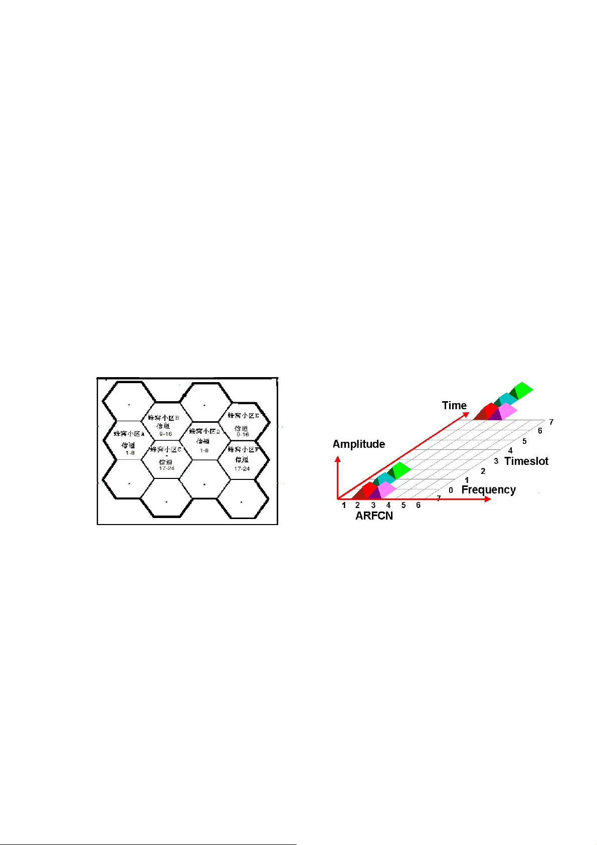
As figure 1 shows, bold line area indicate a overall area covered by a GSM system. The area
was divided into several small cellular cells, each cell has a cellular base station, each base station
occupies a group of given channel.
Figure 1:Cellular sketch map Figure 2:Channel division sketch map
For example, suppose cell A occupies 1 - 8 channels, cell B occupies 9 - 16 channels, cell C
occupies 17 – 24 channels, then cell D can also use 1 – 8 channels same as the cell A, because
they are not close to each other. Then cell E can also occupies 9 – 16 channels and cell F occupies
17-24 channels. As figure 1 shows.
Because the telephone can work on any channel in system, then it can also work in any
cellular cell. Although the mobile just need small power to communicate with base station in a
specific cell, but if the same frequency used in a small area, it may also arouse the problem
6
Page 7

co-channel interfere. Through using the digital modulation, front error correct and equilization
technologies, GSM system can contain more co-channel interfere. This indicate that in GSM
system, the cells occupy the same frequency can get more closer than analog system. Then the
GSM system has better frequency usage and has bigger user capacity.
GSM system adopts TDMA and FDMA modulations, and the whole frequency band is
divided into two bands (uplink band and downlink band). Mobile use the uplink channel to
transmit signal, and base station use the downlink channel to transmit signal. Each channel
occupies 200KHz bandwidth, and is identified by one number as ARFCN. Other than frequency
division, GSM also use time division technology. Each ARFCN is shared by 8 time slots. Each
mobile just occupies one time slot in one ARFCN, then waiting for the corresponding time slot in
the next frame. As figure 2 shows, there are 4 TCH channel, each channel occupies one specific
ARFCN and time slot, 3 TCH channel in one ARFCN, but the time slot is different, the other TCH
channel is on another ARFCN. The data is modulated into the carrier using GMSK methods.
The continuous signal bursts can be transmitted in different frequencies, which is called
frequency hopping. Frequency hopping reduces the influence of RF fading, and improves the
security and secrecy of data link. GSM mobile just need transmit one burst in each frame, doesn’t
need to transmit continuously, so it makes the mobile more effective to save power.
The GSM system can automatically hand over the mobile from one cell to another cell,
which the user doesn’t feel unconvenience. The mobile can detect the signal strength of the
neighbor cell, and if the signal of the neighbor cell is bigger, it will inform the base station, and
the base station will switch it to the neighbor cell. All the procedure is done automatically, so the
user can’t fell it.
4.4 Service area
The GSM operator determine the area in which the user can send and receive call, if the
mobile exceed the area, signal (no operation) appear then the user can not send or receive call,
7
Page 8

if the situation appear when talking, then the call will be interrupted.
The mobile phone’s identity information is stored in the HLR and the VLR of the local GSM
system. The VLR include all the identity information of the local mobile. If mobile roam to
another place, area or country, the identity information will send to the new system’s VLR, which
will verify the information with its original system, if it is right, then the phone can be used in the
new area
.
4.5 GPRS introduction
Comparing the GSM system’s telephone service, GPRS provide the LAN and WAN service,
which provide GSM operator a new market, and provide user new function. GPRS support wide
applications, such as small data irregular transfer, surfing internet and large amount of data
transfer.
GPRS was designed for multipurpose service, which include following character:
1.4.0 Data rate can change from several bit/s to 120Kbit/s, then it is low speed, and also high
speed.
1.4.1 User can long time attach and connect to the GPRS server, the cost occur just when the
data transfer. GPRS operation just like using the office pc, powered on in the morning
and powered off in the afternoon.
1.4.2 The initial response time is faster than the circuit exchange, because the service is
continuous but the user only irregularly uses it. The GPRS server is waiting a hit to
activate, and the user don’t need to reconnect when use it.
1.4.3 GPRS is covering area just like GSM is seamless, and it permits simultaneous several
connections.
8
Page 9

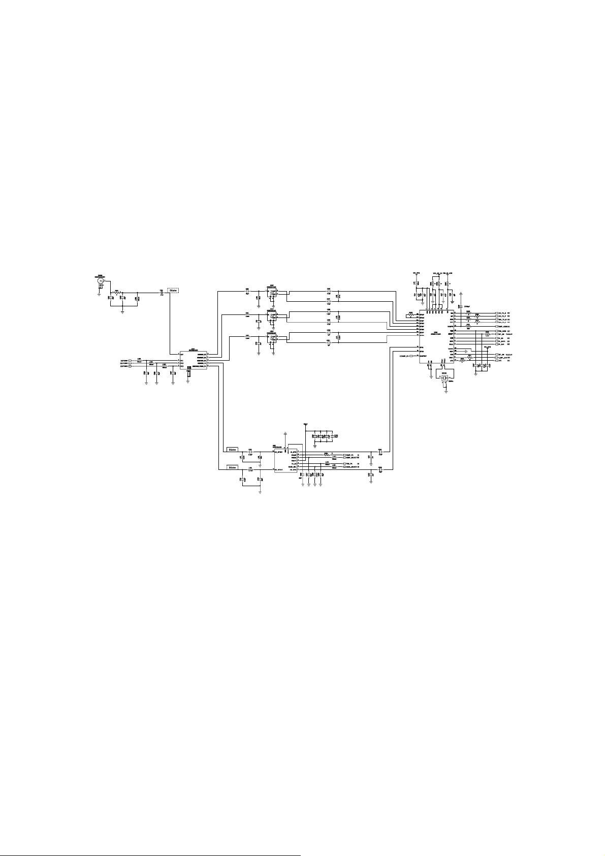
5 ROCK detail schematic circuit
introduction
mobile telephone According to the schematics,there are four parts in ROCK circuit :RF Circuit、
Base band Circuit、Functions Circuit、Connecters Circuit。
5.1 RF circuit introduction
ROCK RF circuit mainly include U106 transceiver chip, U105 power amplifier chip, U102
GSM saw filter, U103 DCS saw filter, U104 PCS saw filter,U101 RF switch module, CN102RF
test connector etc. components. According to function RF circuit can divided to receive path
circuit, transmit circuit and coupling feedback control circuit three parts.
Receive path circuit is mainly composed by U102 GSM saw filter, U103 DCS saw filter,
U104 PCS saw filter,U101 RF switch module, CN102 RF test connector etc. components, U106
transceiver chip. The RF signal first received by the antenna, is sent into the mobile, Then the
signal passes through RF test connector CN101, then passes through the matching circuit
composed of R101, C101 and C102, which used for matching the antenna to the 50 Ohm RF strip
9
Page 10

line. enters into the U101 RF switch module which cotroled by the software when it work for
receiving or transmitting, if it work for receiving, then the signal enters into the U102 GSM saw
filter through the RX1 port or into the U103 DCS saw filter through the RX2 port or into the U104
PCS saw filter through the RX3 port filtering the wanted signal. Then the signal enters into the
U106 transceiver chip through its GSM-RF-IN port or DCS-RF-IN port and PCS-RF-IN,
demodulated into the IQ signal to the U200 baseband chip.
Transmit path circuit is mainly composed of U106 transeiver chip, U105 power amplifier
chip, U101 RF switch module, CN102 RF test connector. The IQ signal generated by the U200
first is modulated into the RF signal in U106 transeiver chip, then it enters the U105 amplifier chip
through the TX900 (GSM) or TX1800 (DCS) or TX1900(PCS) port and matching circuit, then the
amplified signal enter the U101 RF switch module , and then controlled by software transmitted
through antenna.
The function of power control circuit is control the power accord with the GSM specification
transmitted from U105 power amplifier chip.
10
Page 11

5.2 Baseband circuit introduction
Baseband circuit is mainly composed of U200 CPU chip, U306 memory chip, OSC400
32.768KHz crystal. The baseband processing tasks are divided between the DSP and ARM9
processor cores. Many RF controlling signals come from CPU and the working states of a phone
lie on these signals . The received I/Q signals are processed by CPU and recovered to analog audio
signals ,the analog signals converted by MIC are processed by CPU ,then send out by the RF
circuit. U300 memory chip contain s 512Mbits nor FLASH memory and a 12 8Mbits pseudo st atic
RAM memory. The FLASH memory is used to save the system software and all kinds of personal
information, yet the SRAM memory is just used to save the temporary data, if the mobile is power
off, then the data will lose. OSC400 32.768KHz crystal and P400 backup battery all together
provide the clock signal for real time clock. and P400 backup battery all together provide the
clock signal for real time clock.
11
Page 12

5.3 Power management circuit introduction
U401(power management IC) is an integrated circuit used to provides all the power to the
mobile and management of charging circuit. It is completely solution for power supply
generation ,battery management including charging and a subscriber identity module card
interface including supply generation .The device is controlled by a host controller via a 400KHz
I2C serial interface . In this IC a specific module called ”ON/OFF Control” is implemented. It
controls the switch on/off of the mobile.
12
Page 13

5.4 Peripheral driver circuit
ROCK mobile has many additional functions, These functions need further hardware driver
support.
5.4.1 Display and camera
Camera and LCD controlled by the U1101 chip(MV3020SNK). Its working frequency is
24MHz . The MV3020SNK is a highly integrated IC, dedicated to embedded camera applications
(mobile phones). The MV3020SNK exchanges video data with the host processor via a
programmable interface (SPI, 68xx parallel, 8080 parallel interfaces).The MV3020SNK p rocesses
the digitized sensor data up to SXGA format and converts to a high quality compressed JPEG
snapshot. The MV3020SNK is then capable of showing preview to the display through the display
driver and sending (M)JPEG compressed data or uncompressed video to the host processor. An
embedded microcontroller derivative with I/O ports, 2 I2C-bus interfaces, 1Kbyte of RAM and
13
Page 14

32kbytes of program memory is used to control the interfaces. The LCDC chip is in BGA
package
.
5.4.2 LCD backlight and LED
There are 4 LEDs in LCD backlight circuit in series .The IC RT9284 provides power for these
LED and it converts the voltage of main battery to 18.5V if the enable signal GND_LED is
high .We can set the duty of GND_LED to different value to change the lightness of the LCD
backlight.
14
Page 15

5.4.3 Switches (keypad)
The keypads LEDs are powered by the main battery and controlled by the GPO3 of PMU. When
GPO3 is high ,the keypad LEDs are off and low then on.
5.4.4 Audio Subsystem
a) MIC ,Receiver and Speaker The MIC converts the sound signals to analog signals and
15
Page 16

input them to CPU .
These signals are processed in CPU and then sent out by the RF circuit. The RF circuit receives
the RF signals ,these signals are processed in transiver and CPU ,then drive the receiver to
phonate.
When the preset midis and mp3 are played ,the audio signals are outputted from HFR1 and
HFR2 .The signals are amplified by FU1 ,then drive the speaker.
16
Page 17

b) Earphone The earphone detecting depends on the changing of the voltage of AUDIO_DETECT.
The voltage of MIC_BIAS_AUX is about 2.1V, if the earphone is plugged out , the voltage
equals to that of MIC_BIAS_AUX .If the earphone is plugged in , the voltage of
AUDIO_DETECT is about one of two of that of MIC_BIAS_AUX .
5.4.5 Radiogram system
The U902 (TEA5760UK) is a single chip electronically tuned FM stereo radio for low
voltage application with fully integrated IF selectivity and demodulation. The radio is
completely adjustment free and does only require a minimum of small and low cost
external components. The TEA5760UK application software is compatible to the
TEA5761UK software to enable easy design in for customers.
17
Page 18

5.4.6 SIM Interface
SIM interface circuit is suitable for the SIM card of 3V , the connector CN502 is SIM card
holder .SIM_CLK is the clock signal of SIM card ,SIM_RST is the reset signal of SIM card
provided the PMU .The data is transmitted by SIM_I/O between SIM card and PMU .SIM_VCC
and CCGND are the power supply signals for the SIM card provided by PMU .
5.4.7 System Connector
The system connectors include PCB mainboard CN701 and flipboard CN104, and
the two connectors are connected by FPC .By the two connectors and the FPC ,th
e datum transmitted between LCDC and LCD .The following is the schematic of th
e FPC
18
Page 19

6 Mobile measurement fundamentals
Introduction
The below equipments are needed for the general measurement of the GSM mobile: GSM
wireless communications test set: such as AGILENT 8960, CMU200 etc. Antenna adaptor
(SKN4870A), and the additional RF 50 ohm cable and connector Test SIM card (8102430z01)
Full charged battery.
19
Page 20

6.1 Equipment configuration
First, insert the SIM card into the SIM card socket in the back of the mobile, and then put
the battery on the back. Last, use RF cable to connect the adaptor and the input and output port of
the wireless communications test set, and power on the test set and the mobile.
6.2 EGSM measurement step
All the information can be found in the manual of the wireless communications test set.
Ensure that the mobile can establish call with the test set, and then test the below datum as the
legend 1 shows. The test result should be all in the GSM specification, if so the mobile is ok. If
any test is fail, there must be something wrong with the mobile and should be repaired. Below is
the general information about the EGSM test and specification.
EGSM general information
Low channel number: 975 Transmit frequency: 880.2 MHz Receive frequency: 925.2MHz
Middle channel number: 37
Transmit frequency:
897.4 MHz Receive
frequency: 942.4MHz
High channel number: 124
Transmit frequency: 914.8 MHz Receive frequency: 959.8MHz Legend 1:
EGSM test item Lower limit Upper limit
RMS phase error (max power and smallest power) 0° 5°
Peak phase error (max power and smallest power) 0° 20°
Average frequency error -91Hz +91Hz
Power level 7 (29 dBm) transmit power error CH62 -2db +2db
20
Page 21
Power level 10 (23 dBm) transmit power error CH62 -3db +3db
Power level 15 (13 dBm) transmit power error CH62 -3db +3db
RES II (-103 dBm) receive BER (bit error rate) 2%
RES II (-103 dBm) receive FER (frame erase rate) 0.12%
RX_LEV indicate on -100 dBm -104 dB
RX_LEV indicate on -45 dBm -49 dB -96 dB
RX quality <=2 -41 dB
Attention:Transmit average test data should caculate from 10 separate datum .The received signal
should be –85 dBm, when receive test.
6.3 DCS measurement step
Just like the EGSM test, all the information about the DCS test can be found in the wireless
communications test set, and the mobile used to test can establish call with the test set. All the test
results should fufill the specification of DCS, if not then it must be repaired. Below legend gives
the DCS specifications.
DCS General test information
Total number of channels: 374
Low channel number: 512 Transmit frequency: 1710.2 MHz Receive frequency: 1805.2MHz
Middle channel number: 700 Transmit frequency: 1747.8 MHz Receive frequency: 1842.8MHz
High channel number: 885 Transmit frequency: 1784.8 MHz Receive frequency: 1879.8MHz
Legend 2:
DCS test items Lower limit Upper limit
21
Page 22

RMS phase error (max power and smallest power) 0° 5°
Peak phase error (max power and smallest power) 0° 20°
Average frequency error -171Hz +171Hz
Power level 5 (20 dBm) transmit power error CH700 -2db +2db
Power level 10 (10 dBm) transmit power error CH700 -3db +3db
Power level 15 (0 dBm) transmit power error CH700 -3db +3db
RES II (-102 dBm) receive BER (bit error rate) 2%
RES II (-102 dBm) receive FER (frame erase rate) 0.12%
RX_LEV indicate on -100 dBm -104 dB
RX_LEV indicate on -45 dBm -49 dB -96 dB
RX quality <= 2 -41 dB
6.4 PCS measurement step
Just like the DCS test, all the information about the PCS test can be found in the wireless
communications test set, and the mobile used to test can establish call with the test set. All the test
results should fufill the specification of PCS, if not then it must be repaired. Below legend gives
the PCS specifications.
PCS General test information
Low channel number: 512 Transmit frequency: 1850.2 MHz Receive frequency: 1930.2MHz
Middle channel number: 661
Transmit frequency:
1880 MHz Receive
frequency: 1960MHz
High channel number: 810 Transmit frequency:1909.8 MH z Recei ve frequency: 1989.8MHz
22
Page 23

Legend 3:
Pcs test items Lower limit Upper limit
RMS phase error (max power and smallest power) 0° 5°
Peak phase error (max power and smallest power) 0° 20°
Average frequency error -171Hz +171Hz
Power level 5 (20 dBm) transmit power error CH700 -2db +2db
Power level 10 (10 dBm) transmit power error CH62 -3db +3db
Power level 15 (0 dBm) transmit power error CH62 -3db +3db
RES II (-102 dBm) receive BER (bit error rate) 2%
RES II (-102 dBm) receive FER (frame erase rate) 0.12%
RX_LEV indicate on -100 dBm -104 dB -96 dB
RX_LEV indicate on -45 dBm -49 dB -41 dB
RX quality <= 2
7 Trouble shooting
7.1 Attentions
Because the ESD sensitive components in the mobile, then the mobile should be repaired
in the ESD protection environment which should be configured as below:
Working desk --- All the desk should cover ESD protection mat, and should connect with
a 1.2 M Ohm resistor to the ground.
Hand ring --- Connected with a soft line which can quickly release the static electron,
and also connect with a 1.2 M Ohm or 5.2K Ohm resistor to the ground.
23
Page 24

7.2 Repair equipments and tools
Suggest using the below equipments and tools to repair:
1. AGILENT8960 / CMU200 — GSM wireless communications test set
2. AGILENT8594E — Frequency spectrometer
3. AGILENT54520 — Oscillograph
4. AGILENT34401A — Universal meter
5. LPS-105—AMRFL direct current power
6. HAKO926 — Electric iron
7. HAKO851 – Temperature controlled electric dryer
8. Computer ( with GPIB card)
9. 50 Ohm cable line 、N160 back plug line
10. Level shifter box — Provided by Techfaith Electric iron temperature/time
Normal weld spot: 350°±10°,<= 5 seconds: Big weld spot: 400°
±10°,<=5 seconds
Electric dryer temperature/time 295°±5°,<= 120 seconds 395°±5°,<= 30 seconds The
repair equipments configured as below figure shows:
Repair station configuration
The computer preinstalled Dragonfly lab test studio software connect with power supply
and the wireless communicati ons test set through GPIB, connect with the le vel shift box through
24
Page 25

serial cable, and the level shift box connect with mobile through back plug line, connect with the
wireless communications test set through 50 Ohm RF cable.
7.3 Phone repair
The whole phone repair mainly repair the phone which can’t pass the CIT function test
and call test and antenna test. The ordinary function fault inculd: can’t power on, receiver no
sound, microphone no voice, no vibration, speaker no sound, camera abnormal display, tuchpanel
no function and keys no function etc; call test and antenna test generally including: can’t establish
call and test results beyond specification.
7.3.1 Receiver no sound, microphone no voice
Receiver no sound and microphone no voice can use the loopback CIT function determine
where is the problem. If the loopback test is ok, then the loopback circuit (receiver and
microphone circuit) is ok. If the loopback is no function, then please make a 112 emergency call
or another public numbers, if the receiver is no sound then the receiver circuit has something
wrong, if the receiver has sound then the microphone is bad.
If the receiver is no sound, first use a good receiver change it, if it is ok, then change it, if the
receiver is still no sound, then check the solder, whether it has solder problem.
If the microphone has problem, also first use a good microphone do the replace experiment, if
it is ok, just change it. If still no voice, then check the microphone circuit.
7.3.2 Incapable power on
Battery no power, battery connector damaged or bad solder, or the pcb has something
wrong may cause the problem incapable power on. If it is the problem of the battery connector P2,
then resolder it or change it is ok. If it is not the problem of battery connector, then use a universal
meter to measure the “+” pole of the P2 connector, check whether it is shorted to the ground, if
25
Page 26

shorted please check the board. If the “+” pole is not grounded then use a good LCD module to do
the replace experiment, if the mobile can power on now, then should change the LCD module. If
the mobile still can’t power on then there must something wrong with the pcb, please retest the
PCB board, if the test pass then redownload software can get rid of it, if the test fail, then should
repair the PCB as the following chart introducing methods.
7.3.3 LCD abnormal display
Abnormal display usually behaves like as: white screen, no backlight, blur screen or
abnormal color. First check if it is the problem of LCD module, change a new one if the problem
disappear then it is the problem of the LCD module, if the problem still exists then check the main
26
Page 27

connector CN801 on main board whether it is broken or bad solder, then resolder it or change it. If
it is not the problem, according to the following chart introducing methods, it can resolve these
problems.
27
Page 28

7.3.4 Speaker no sound
First enter the CIT test mode, if the speaker is ok, then you should reinitialize the software. If
the speaker has no sound, then use a good speaker to do the replace experiment, if the new speaker
has sound, then change speaker is ok, if the new speaker is also no sound, then should check the
solder of speaker and resolder can resolve the problem. If the problem still exists then check the
chip U601 on main board whether it is broken or bad solder, then resolder it or change it. After
checking all these is ok, The speaker circuit will be checked and well CPU should be checked
.
7.3.5 Camera abnormal function
Repair the camera just like repair the LCD abnormal display, first check if the CN802
camera connectors is ok, if it is ok, then use a good camera do the replace experiment, if the
problem still exist,. After checking all camera circuit are ok, then U1101 (MV3020SNK ) should
be checked. And also sccoding to the following chart introducing methods to repair this issue.
28
Page 29

7.3.6 Mobile can’t identify the SIM card
First make sure the SIM card is not damaged, use a good SIM card to test if the problem still
exist. If still exist, then check if it is the problem of the SIM card socket, change it or resolder it. If
it is not the problem of the socket, then it is always the problem of U401(PMU) chip, resolder it or
change it can always resolve it.
7.3.7 No vibration
First check if the speaker lines wind the vibrator, if not, use a digital power tuned to the
2.75V adding to the two poles of the vibrator, see if the vibrator vibrate, if not then it shows
that the vibrator damaged, change it. If it vibate, then check if the D509 have been shorted, if
shorted, resolder it. Measure the voltage of D509 ,if not 3V, then it is the problem of U401
PMU chip, resolder or change it.
29
Page 30

7.3.8 Key press no function
ROCK mobile just have 21 keys. If only one key no function, please disassemble the mobile
back housing, check if the metal dome damaged or the corresponding pad is dirty. If there are 4 or
5 or multiple key no function, the root cause is CPU unsoldered or fault.
7.3.9 RF trouble shootin
For RF problems ,it’s generally caused by RF circuit, and should be checked. CN102 (RF
test connector), U101 (RF switch module), U105(power amplifier module) and U106(transeiver).
If any component has problem, resolder or change it will resolve the problem. If the RF path is ok,
then check the OSC100 (24MHz oscillator) , reflow or change the part will get rid of this problem.
The detail RF path check steps as below:
First connect the PCB board to the configuration (Repair station configuration ), plug
the back-plug, and then open the Dragonfly debug tool, select the TX path check in the catalog of
Factory test, input the channel number, and adjust the transmit power value(5-19), and then hit the
“start transmit” button, make the mobile on the transmit condition, then adjust the frequency of the
Frequency spectrometer to the transmit frequency, measure R101,check if the output power of
R101 is right. If the power is right shows that the RF path is no problem,if the power is abnormity
then should check the CN102,measure C103, if the power is right shows that the CN102 RF test
connecter is not ok .resolding or changing another one should be done; if the power is abnorm ity
then should check the U101 RF switch module,measureL120 GSM band and R106 DCS/PCS
band. check the output power of L120 and R106,if the power is right shows that U101 RF switch
module is no problem. If the power is abnormity then should check U105 RF PA, measure L121
and R108, check the output power of L121 and R108, if the power is right shows that U105. RF
PA is no problem. If the power is abnormity then should check U110 measure C151 and C153,
30
Page 31
check the output power of C151 and C153,if the power is abnormity then should check OSC100
clock circuit and U110,resold or change it ,the problem will be resolved ,if can’t,U200 CPU
should be checked. For the method checking the RX path, it’s the same with checking Tx path.
And also accoding to the following chart introducing methods to repair.
7.4 schematics
31
Page 32

32
Page 33

33
Page 34

34
Page 35

35
Page 36

36
Page 37

37
 Loading...