

Page 1

Ienovo i909
Mobile Phone
Maintenance Manual
LENOVO
Page 2

I908 Mobile Phone Maintenance Manual LENOVO
File name: Lenovo i909 Mobile Phone Maintenance Manual
Edition: V1.0
Date: September 7, 2007
File No.:
Status:
Preface
This is an instruction manual used as a maintenance guide for Lenovo I909 both during
producing and after sale.
This manual is subject to modifications as is deemed necessary by further
technological development.
copyright statement
The copyright for this manual is the property of Lenovo Mobile Communication
Technology Ltd. Any person that duplicates this manual without Lenovo’s written approval
will be liable to prosecution.
Page 2
Page 3

I908 Mobile Phone Maintenance Manual LENOVO
Table of Contents
1 PHONE EXTERIOR......................................................................................................................5
2 MAIN BOARD LAYOUT...............................................................................................................7
COMPONENT SIDE: ............................................................................................................................7
3 BASEBAND...................................................................................................................................9
3.1 LCD DISPLAY...........................................................................................................................9
3.1.1 No display after the phone is turned on.........................................................................9
3.1.2 The LCD backlight does not come on......................................................................10
3.2 RINGING AND VIBRATION .......................................................................................................11
3.2.1 The unit does not vibrate...............................................................................................11
3.2.2 No ringing sound..............................................................................................................1
3.3 CHARGING .............................................................................................................................13
3.3.1 The charger has been connected to the phone, but there is no charging display on
the screen.....................................................................................................................................13
3.3.2 The screen shows that the phone is charging, but the battery cannot be fully
charged
3.4 KEYP AD AN D KEYPAD BACKLIGHT.........................................................................................15
3.4.1 The keypad does not work normally............................................................................15
3.4.2 The keypad backlight is inactive...................................................................................16
3.5 IN CALL ISSUES........................................................................................................................1
3.5.1 The voice of the person on the other end of the line can’t be heard.......................17
3.5.2 The person on the other end of the line can’t hear my voice...................................18
3.6 THE PHONE CANNOT BE POWERED ON.................................................................................19
.........................................................................................................................................14
4 RADIOFREQUENCY (RF).........................................................................................................20
4.1 PROBLEMS DURING SOFTWARE DOWNLOAD........................................................................20
4.2 PRODUCTION CALIBRATION...................................................................................................21
4.2.1 AFC calibration................................................................................................................21
4.2.2 Rx path loss........................................................................................................................22
4.2.3 PCL....................................................................................................................................22
4.3 TESTING OF THE UNIT/PROBLEMS DURING REPAIR..............................................................24
4.3.1 Switch Spectrum and Ramp Mask overrun...................................................................24
4.3.2 Significant frequency error................................................................................................25
4.3.3 Significant phase error ......................................................................................................25
4.3.4 Power output problems..................................................................................................26
5 ASSEMBLY AND DISASSEMBLY OF THE I909...................................................................28
5.1 TECHNICAL STEPS FOR I909 ASSEMBLY...............................................................................28
5.2 I909 PARTS LAYOUT ..............................................................................................................30
5.3 PRECAUTIONS DURING THE ASSEMBLY OF THE I909............................................................31
Page 3
Page 4

I908 Mobile Phone Maintenance Manual LENOVO
Date of
Edition
No.
Compiled by/
Modified by
compilatio
n/modifica
Reasons for
modification
Main Changes
tion
Page 4
Page 5

1 Phone Exterior
Figure 1.1 Frontal view of the unit
Page 6
I908 Mobile Phone Maintenance Manual LENOVO
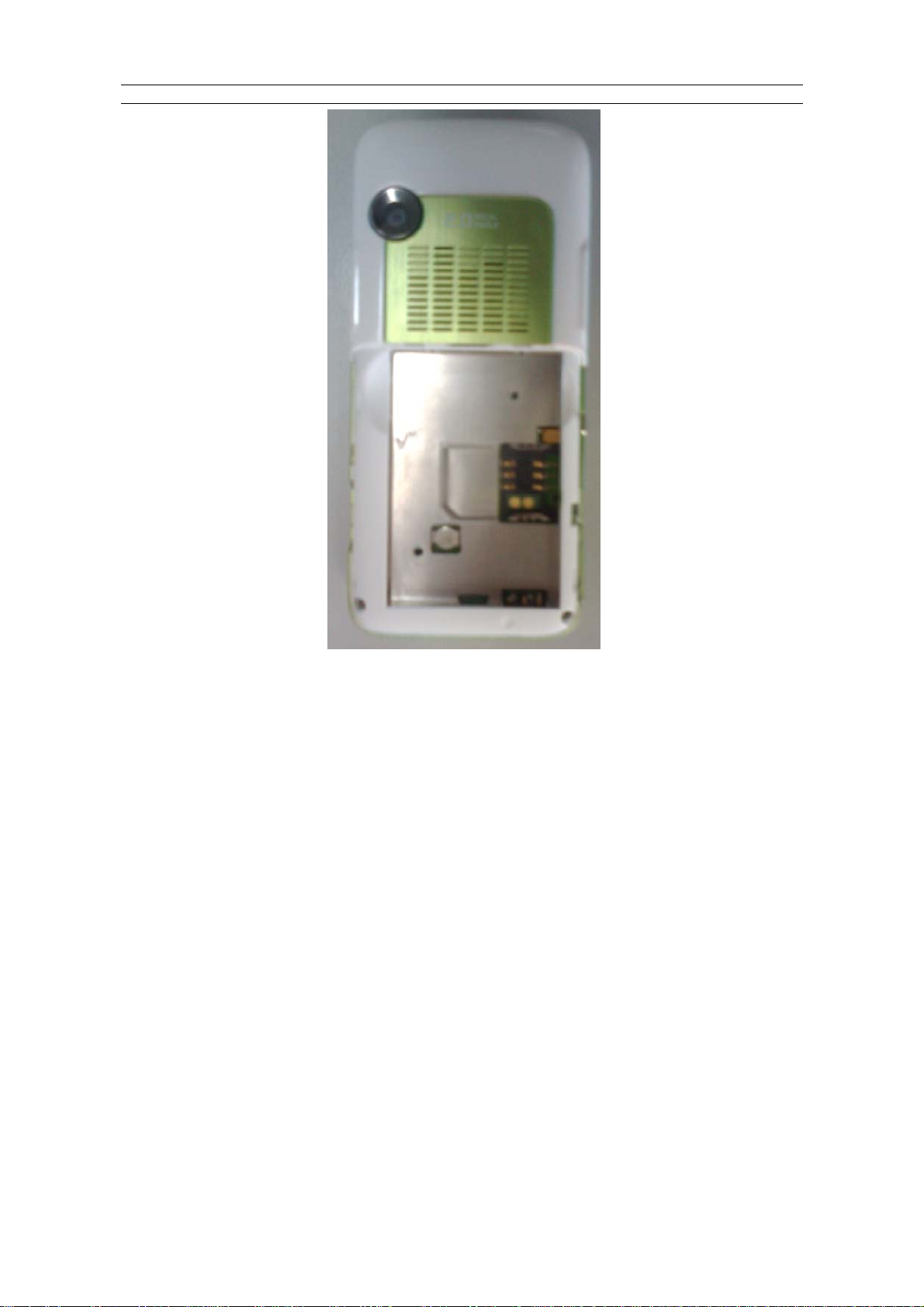
Figure 1.2 Figure 1.2 Rear view of the unit (battery removed)
Page 6
Page 7
I908 Mobile Phone Maintenance Manual LENOVO
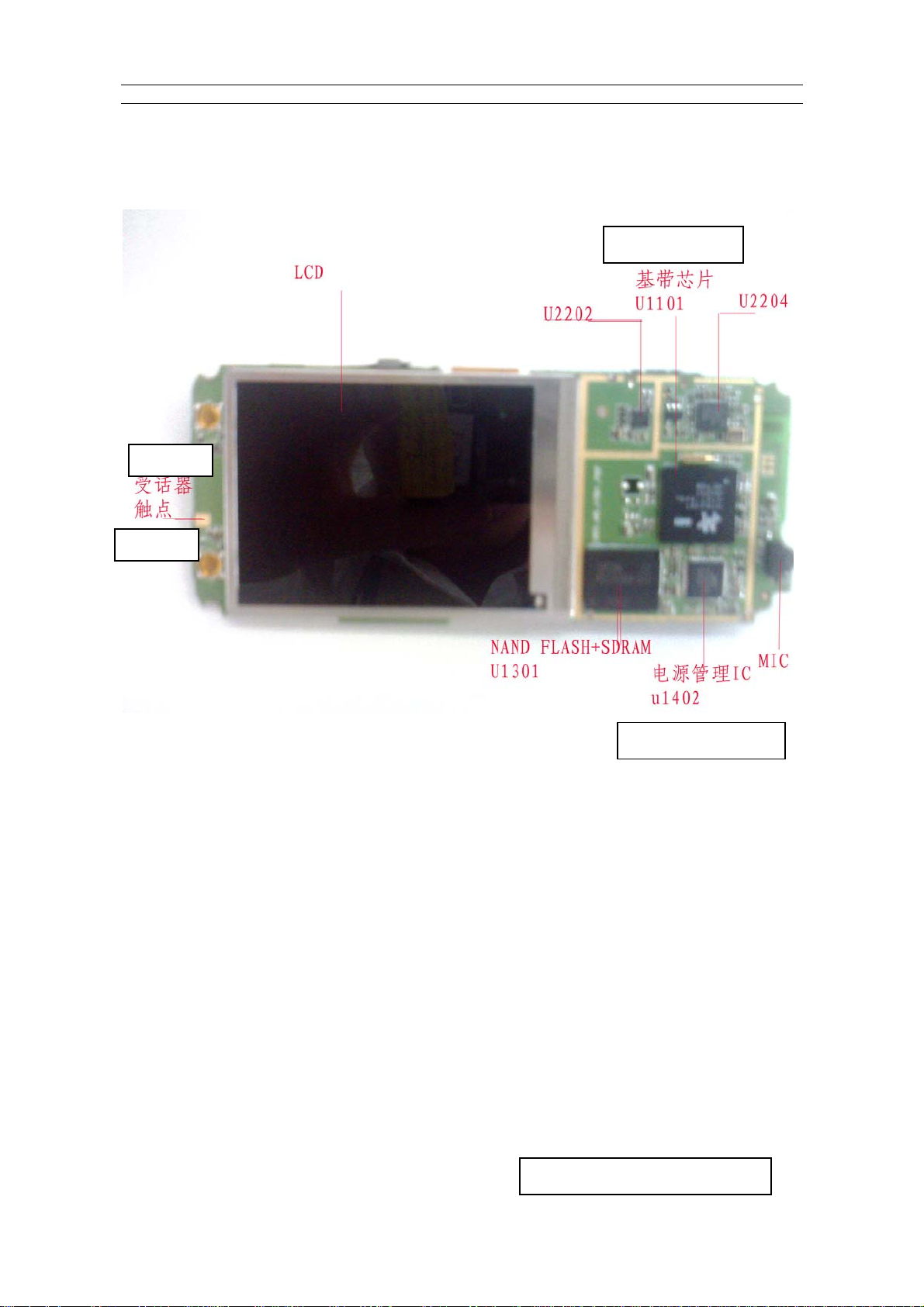
2 Main Board Layout
Component Side
Receiver
Contact
:
Baseband Chip
Power Management
Double-SPK Pin Connector
Page 7
Page 8
I908 Mobile Phone Maintenance Manual LENOVO
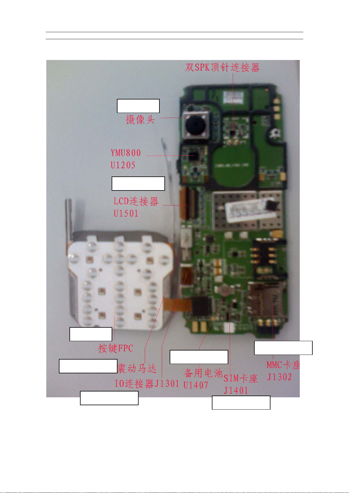
Keypad Side:
Camera
LCD Connector
Vibration Motor
Keypad FPC
I0 Connector
MMC Card Socket
Stand-by Battery
SIM Card Socket
Page 8
Page 9
I908 Mobile Phone Maintenance Manual LENOVO
3 Baseband
3.1 LCD Display
3.1.1 No display after the phone is turned on
Y Y
Check the FPC and the main
board connection. Re-connect
and try again
Check for such soldering
problems as pseudo soldering and
bridging at the ports of the LCD
The screen does
OK
N
Y
OK
N
Replace LCD
Page 9
Page 10

I908 Mobile Phone Maintenance Manual LENOVO
g
g
3.1.2 The LCD backlight does not come on
Check the FPC and the main
board connection. Re-connect
and try again
Check for such soldering
problems as pseudo soldering
and bridging at the ports of the
Check whether the output of
backli
Replace L1502 or U1508 and
check for the solderin
LCD backlight
inactive
N
N
ht circuit is above 9V.
N
at
OK
Y
OK
Y
Replace LCD
Y
OK
Page 10
Page 11

I908 Mobile Phone Maintenance Manual LENOVO
3.2 Ringing and Vibration
3.2.1 The unit does not vibrate
Check for the connection of
The unit
N
Replace motor
Y
OK
Page 11
Page 12

I908 Mobile Phone Maintenance Manual LENOVO
3.2.2 No ringing sound
Y
N
Identify the SPK that makes no
sound. Check the speaker
connection or replace the speaker .
No ringing
N
Check whether U1205,
U1206 and U1207
N
Replace U1206
OK
OK
Page 12
Page 13

I908 Mobile Phone Maintenance Manual LENOVO
y
3.3 Charging
3.3.1 The charger has been connected to the phone, but
there is no charging display on the screen
No charging
prompt after
Is there still a problem
when another charger is
N
Is there still a problem
when another batter
N
Check the soldering at
U1408 and J1301.
Re-solder and see if it
N
Replace
is
Y
Replace
Y
Replace
Y
OK
Page 13
Page 14

I908 Mobile Phone Maintenance Manual LENOVO
p
3.3.2 The screen shows that the phone is charging, but the
battery cannot be fully charged
Y
N
Y
Y
N
The charging
indictor is
Check for soldering
faults at U1408,
J1301 and U1402.
Touch u
Replace U1408.
Replace U1402.
Replace battery
and try
N
N
OK
OK
OK
Page 14
Page 15

I908 Mobile Phone Maintenance Manual LENOVO
3.4 Keypad and Keypad Backlight
3.4.1 The keypad does not work normally
N
Y
N
Disassemble the mobile
phone to check the connection
Open up the phone and
check if the metal dome is
Remove the metal dome
and clean the keypad with
alcohol. Attach a new dome
The
Fix or
replace
metal
Page 15
Page 16

I908 Mobile Phone Maintenance Manual LENOVO
3.4.2 The keypad backlight is inactive
Y
N
Y
N
The keypad
Some of the
Check the FPC for
possible pseudo
Replace
the FPC
Replace the
damaged
OK
Page 16
Page 17

I908 Mobile Phone Maintenance Manual LENOVO
3.5 In Call Issues
3.5.1 The voice of the person on the other end of the line
can’t be heard
Y
N
The voice
of the
Remove the upper
cover and check
Replace
Replace
Page 17
Page 18

I908 Mobile Phone Maintenance Manual LENOVO
3.5.2 The person on the other end of the line can’t hear my
voice
My voice can’t
Y
N
Y
N
Y
N
Remove the lower cover
and check MIC for any
Replace the MIC and try
Check
U1212/R1204/R1209/C121
0/C1211/R1203/R1216 for
possible pseudo soldering
Check
Re-so
OK
Re-s
Page 18
Page 19

I908 Mobile Phone Maintenance Manual LENOVO
3.6 The Phone cannot be Powered on
Firstly check U1402 for pseudo
soldering. Is the output of
VTCXO, VCORE, VMEM and
Are there soldering
The
Y
Is U2107 normal at
26MHz?
Y
N
N
Re-solder
U1402
N
Check for pseudo
Y
Touch up
N
Re-solder
Check the U2106
Page 19
Page 20

I908 Mobile Phone Maintenance Manual LENOVO
p
g
g
4 Radiofrequency (RF)
4.1 Problems during Software Download
z Problem: The software cannot be downloaded properly.
z Causes: The baseband chip has been fitted the wrong way round or there are problems
with the soldering point; Pseudo soldering on CRYSTAL.
z Solution:
The software
cannot be
Check whether the baseband
chip has been fitted the wrong
N
Check U1101 for possible pseudo
N
Check whether the crystal (X2101)
N
Respectively check X2101 and C2104 and C2148 of
U2101 at Pin31for
z Please re-download the software after replacing the defective assemblies.
ossible pseudo solderin
Re-solder the pseudo
solderin
assemblies
Y
Re-solder U1101
Y
Re-solder U1101
Y
Re-solder X2101
Page 20
Page 21

I908 Mobile Phone Maintenance Manual LENOVO
p
4.2 Production Calibration
4.2.1 AFC calibration
z Problem:AFC calibration failed.
z Causes: RF test cable is not connected properly during calibration; the crystal and its
peripheral circuits (AFC power supply) have been fitted the wrong way round or there are
problems with the soldering points.
z Solution:
AFC calibration
failed
Check whether or
not the RF wire and
Y
Check whether the
N
Check the crystal (X2101) for
ossible pseudo soldering
N
Check whether there is
Y
Recalibrate
N
Re-connect and
Y
Re-solder X2101
Y
N
Replace PA (U2102)
Re-solder X2101
z Please note: Calibration usually has to be repeated after the assembly (assemblies) has
(have) been replaced.
Page 21
Page 22

g
r
(
Re-sold
r
rrep
er L2101
Re-solder
o
replace
Replace
and
I908 Mobile Phone Maintenance Manual LENOVO
4.2.2 Rx path loss
z Problem:Rx path loss calibration failed.
z Causes: RF test cable is not connected properly during calibration; Pseudo soldering with
assemblies on the receiver channel, such as the antenna connector, antenna switch, saw
filter and the surrounding peripheral capacitors.
z Solution:
Y
Y
Y
z Please note: Calibration usually has to be repeated after the assembly (assemblies) has
(have) been replaced.
Did the
GSM
Y
Check the Saw
filter (Z2101)
for pseudo
N
Check
C2128,C2129 and
N
Check the
N
N
Check
L2110
Check the
Saw filter
Z2102) for
Check C2107,
C2130 and
L2111 for
Rx path loss
calibration
Check the calibration
report and see
Y
Re-sold
e
L2110
N
Y
N
N
Y
Re-solder
o
lace
Y
Check whether or
not the RF wire and
Y
Check for pseudo
solderin
Check C2108 and the
antenna switch
at the
N
N
Y
Y
Re-conne
ct and
Re-sold
er U2105
Re-sold
er C2108
4.2.3 PCL
Problem1
Page 22
Page 23

I908 Mobile Phone Maintenance Manual LENOVO
solde
z Problem:PCL Calibration failed.
z Causes: RF test cable is n ot connected properly during calibration; PA has been attached the
wrong way round; PA and the surrounding circuits have soldering-point problems; chips on
the RF input circuits of the PA are displaced. Circuits are short connected with the shielding
frame.
z Solution:
PCL calibration
Y
Check whether
or not the RF
Y
Is there any
pseudo soldering
N
Did the PA
N
Is there any
pseudo
N
Check the baseband
Y
Y
N
Y
R-connect
and
Solder
U2105 and
Re-solder
U2102
Replace
and solder
Sold
er
Sold
er
Y
There is
soldering
Y
Is there any
pseudo
soldering at
the PA input
Z2103?
Did the
Y
N
N
N
Did the DCS
Is there
Check the
Y
Y
ring
Replace
z Please note: Calibration usually has to be repeated after the assembly (assemblies) has
(have) been replaced.
Problem2:
z Problem: Phone power output too high
z Causes: This is usually due to the wire not being connected properly during calibration.
z Solution:
Power too high
Check the RF wire and
clip. Ensure that they
Re-connect and
Page 23
Page 24

I908 Mobile Phone Maintenance Manual LENOVO
Problem 3:
z Problem: After several times of calibration, the output power is still higher than normal. And
then PA is damaged.
z Cause of the Problem: PA and chips of VA PC input assemblies are out of position. PA is
damaged.
z Solution:
Is the voltage of PA (U2102) at Pin6 far
higher than 1.4V?
4.3 Testing of the Unit/Problems during Repair
After several times of
calibration, the output
Y
Are the upper parts of
C2105 and R2104
N
Replace PA
(U2102) and
repeat
N
Replace PA
(U2108) and
4.3.1 Switch Spectrum and Ramp Mask overrun
z Problem: The switch spectrums and ramp ma s ks of both GSM and DCS bands exceed the
limits.
z Cause of the Problem: If R2103 (10K Ohm), R2104 (18K Ohm) or the capacitor C2105 (220pF)
on the V_ ramp signal cable of the PA are not soldered properly or damaged, this will cause
the frequency and spectrum to exceed norms.
z Solution:
PA may be damaged. Replace
C2105, R2104 and PA (U2104). Then
Switch Spectrum
and Ramp Mask
Does the voltage of PA (U2102) at Pin6 falls
within the normal range (less than 1.8V)?
Check C2105 and R2104
(critical point) for possible
Replace elements with
pseudo soldering.
Page 24
Page 25

I908 Mobile Phone Maintenance Manual LENOVO
4.3.2 Significant frequency error
z Problem: Frequency errors during the testing of the unit exceed norms.
z Cause of the Problem: 1) Problems with AFC calibration
z 2) Crystal was reversely attached. Damage or pseudo soldering
z Faults Solution:
Frequency Error exceeds the
norms
Recalibrate
Check X21015 for possible
Replace elements with
4.3.3 Significant phase error
z Problem: The phase error during the testing of the unit exceeds norms and the ORFS
spectrum exceeds norms between 0-10 bits.
Page 25
Page 26

I908 Mobile Phone Maintenance Manual LENOVO
z Cause of the Problem: The capacitors of the PA and transceiver power supply sections have
faulty soldering points or are short circuited with other resistors.
z Solution:
Check the power supply circuitry of
PA (U2102) and the Transceiver
Phase Error overruns
Replace elements
4.3.4 Power output problems
z Problem: The unit can be turned on and receipt is normal, however, there is no power
output, or power output is low when dual or single power frequencies are output
z Causes: Many causes can lead to no or little output power, such as signal failures or circuit
troubles with the transceiver output section, PA I/O circuit, antenna connector and antenna
switch control. Cause of the Problem:
Antenna Connector (U2105)
Check: Check the connection between the antenna connector U2105 and RF test probes.
Alternatively, check whether or not the chip has been attached in the wrong direction or if the
antenna connector is damaged.
Solution: Replace the antenna connector and make sure that the chip is attached in the
right direction.
Antenna Switch (U2104)
Check: Check for pseudo soldering at the antenna switch U2104 and its peripheral circuits,
pay special attention to the magnetic beads L2114 and L2104 on the pins (Pin2, Pin10) of the
antenna switch control signal.
Solution: Replace pseudo soldering assembly (assemblies)
RF Power Amplifier (PA)
Check whether or not the control signal of the P A (PA_EN (pin3)) is at a high voltage, i.e.
around 2.8V;If it is at a low voltage, then the PA has no output; Check the
series-wound 1K ohm resistor R2102 for possible pseudo soldering or disconnection
again.
Check the power supply of PA at Pin4 to see whether the voltage is within normal
range (normally 3.6V~4.2V);
Check RF input parts of PA, such as Z2103, L2106 and L2107 for possible pseudo
soldering;
Page 26
Page 27

I908 Mobile Phone Maintenance Manual LENOVO
Check whether or not there is pseudo soldering at L2108 and L2109 of the RF output
of PA;
V_ramp signal control circuit of PA:If there is pseudo soldering or disconnection
among R2103 (10K ohm), R2104 (18K ohm) and capacitor C2105(220pF), there will
be no power output from the PA.
Transceiver (U2101)
Check the power supply voltage of the transceiver (U2101). C2103, C2131, C2142, C2144,
C2147 and C2154are the filter capacitors of the transceiver power supply terminal. Check
the voltage at the connections between these capacitors and the transceiver. Then
check the peripheral circuit for possible pseudo soldering.
If the condition of the unit allows, it can be put into normal mode with full power output. Use
a frequency spectrometer analyzer to measure the output power of the various modules on the
launch circuit.Normally:
A. Power output of about 33dBm of GSM or 30dBm of DCS can be detected at the
power output terminal of the antenna connector.
B. Power o utput of about 33dBm of GSM or 30dBm of DCS can be detected at the
connecting point between the antenna switch power output terminal pin9 and
C2108;
C. Power output of about 32dBm and 30dBm can be respectively detected at the
joint of pin 8 and pin 9 of output terminal of PA;
D. Power output of around 4dBm can be detected at pin38 and pin39 of the transcei ver
output terminal.
This should be helpful in determining the nature of the problem. Please deal with the
problem accordingly.
Page 27
Page 28

I908 Mobile Phone Maintenance Manual LENOVO
5 Assembly and Disassembly of
the i909
5.1 Technical Steps for i909 Assembly
Fig. 5-1 The assembly break down of the i909
As is shown in Figure 5-1:
Install the camera 12 to
the camera protective cover 14
the camera connector of main board 10, cover
and dust-proof cover 15;
Attach the seal foam of sound cavity 13 on the main board 10;
Attach Speaker insulators 32
on the back of the 2 speakers 31
respectively, then attach a keypad connector pad 34 to one of the
speaker insulators
insulator32;Attach a keypad connector pad 34
32 and a speaker pad 35 to other speaker
on the back of the
speaker
33;
Install the three speakers respectively to the antenna assembly 16 and
Page 28
Page 29

I908 Mobile Phone Maintenance Manual LENOVO
then clip the whole antenna assembly 16 on the main board10;
Attach the shielding cover conductive cloth 41 to the lower metal frame
of LCD8 and then cover the back of the metal frame; attach LCD
conductive back glue 9 on corresponding positions on the main board
10; after attaching the conductive double-sided glue 38, install the LCD8;
then attach
side wall
Attach the wave-absorbing material 40
magnesium alloy shielding cover
corresponding positions on
shielding cover
magnesium alloy
the other end of the conductive double-sided glue 38 to the
of antenna assembly 16;
to the back of the of the
39; attach the keypad DOME42 on the
FPC43; attach the conductive cloth 41 of the
to the lower part of LCD8 where it connects with the
39; attach the keypad FPC43 to the magnesium alloy
shielding cover 39;
Install the microphone cover 37 to the microphone on the main board 10,
cover the magnesium alloy shielding cover 39, clip the keypad FPC43
connector on the main board 10, clip the keypad connector pad 34, and
lock with 4 screws 36;
Install the LCD buffer foam7, receiver dust-proof net 3 and receiver 6 on
the corresponding positions on front housing assembly 5, and install the
Play A keypad 2, Play B keypad 4 and main keypad 44;
Install the Music Keypad 17, V olume Keypad 20, Capture Keypad 28, IO
cap 29 and TF cap 30 respectively on the corresponding positions on
Page 29
Page 30

I908 Mobile Phone Maintenance Manual LENOVO
the rear housing assembly 19;
Fit the main board 10
into the rear housing 19. Make sure that it is fixed
in the correct position and that none of the keys are obstructed when
pressed.
Assemble the rear housing assembly 19 with the front housing
assembly 5. Make sure that 4 screws 18 are locked on the
corresponding positions on the rear housing assembly;
Attach the sound cavity seal foam 21
23 to the corresponding positions
assembly
22 and fix the rear housing decoration assembly 22 on the
and camera decoration assembly
on the rear housing decoration
back of the rear housing;
Attach the main lens
assembl
y 5
Attach the seal pad 27
housing and paste the main body label 26
1 at the corresponding position in the front housing
to the corresponding positions on the rear
on the battery cabin on the
rear housing;
Place the built-in battery (25) in the phone and clip the battery cover
(24).
5.2 i909 Parts Layout
5.2.1 Location of main label on the Rear Housing
Page 30
Page 31

I908 Mobile Phone Maintenance Manual LENOVO
5.3 Precautions during the Assembly of the i909
i.Make sure that the camera connector is properly connected to the
connector housing of the main board when installing the camera
ii.Make sure that each clip is in proper connection with the main body
when installing the antenna components
iii.The FPC keypad
positioning holes on the magnesium alloy screen cover.
and the DOME keypad must be aligned with the 7
iv.Please note that the side keys should be able to be pressed in
without obstruction when you are fitting the main board.
v.For disassembling the rear housing, please remove the decoration
component of the rear housing before removing the 4 screws;
Page 31
Page 32

I908 Mobile Phone Maintenance Manual LENOVO
vi.During the assembly of the LCD, it is important to make sure that the
of the LCD is inserted into the FPC connector properly;
FPC
otherwise there may be display problems.
Page 32
 Loading...