

Page 1

MASS2 Technical Manual
1. Product Specification
2. Mechanical Construction
3. Circuit Description
4. IC Information
5. Spare Part List
6. Map
7. Schematic
8. Block diagram
- COMPANY CONFIDENTIAL -
Ezze Mobile Tech., Inc
Fax.
Tel. +82 (0)2 519 7700
+82 (0)2 519 7882
Page 2

Section 1 – Product Specification
Contents Page
MASS2 specifications ..……...…………..………………………………………..…… 1.1
Batteries …………………………..………………………………..……………………. 1.3
Standard charger………………………………..…………….………………………… 1.5
- COMPANY CONFIDENTIAL -
Ezze Mobile Tech., Inc
Fax.
Tel. +82 (0)2 519 7700
+82 (0)2 519 7882
Page 3

Section 2 – Mechanical Construction
Contents Page
Disassembly ……………………………………………………………………………... 2.1
Phone disassembly …………………………..……………………………….……… ... 2.2
Phone Assembly ………………………………………………………………………… 2.7
- COMPANY CONFIDENTIAL -
Ezze Mobile Tech., Inc
Fax.
Tel. +82 (0)2 519 7700
+82 (0)2 519 7882
Page 4

Section 3 – Circuit Description
Contents Page
Baseband section …………………………………………………………………..……… 3.1
MT6225 ( GSM/GPRS Baseband processor ) …………..…………………….………… 3.1
MT6318 ( GSM Power Management System ) ……………………………..…….……. 3.38
PF38F3040L0ZBQ1( MCP) …… … …………. …… … …………………………………..3.46
RF section ............................................................................................................................... 3.48
MT6120 ( RF Transceiver IC ) ………………………………………………………….… 3.48
RF3166 ( QUAD-BAND Power Amplifier Module ) …………………………………..3.55
LMSP54HA-348TEMP ( Antenna Switch Module for Tri Band ) ……………….….. 3.58
- COMPANY CONFIDENTIAL -
Ezze Mobile Tech., Inc
Fax.
Tel. +82 (0)2 519 7700
+82 (0)2 519 7882
Page 5

Section 4 – IC Information
Contents Page
Pin out for U 900 …………………………………………………………...……….….. 4.1
Pin out for U 901 …………………………………………………………...……….….. 4.2
Pin out for BAT 300 …………………………………………………………...……….. 4.3
Pin out for CON 300…………………………………………………………...……….. 4.4
Pin out for CN 130 ……………………………………………………………...………. 4.5
Pin out for U 2 ……………………………………………………………...……….… 4.6
Pin out for U 820……………………………………………………...……….……….... 4.9
Pin out for U910…………………………………………………………...……….…..... 4.11
Pin out for LED701~LED706……………………………………………...……...……. 4.12
Pin out for OSC100…………………………………………………………...……….… 4.12
Pin out for U300…………………………………………………….………...……….… 4.13
Pin out for D100,D300,D800…………………………………………...…………..…… 4.17
Pin out for U302 ………………………………………………………………………… 4.18
Pin out for U301…………….. …………………………………………………………… 4.19
Pin out for ZD101,ZD102 …….… …………………………………………….………. 4.19
Pin out for ZD100,ZD106 …………………………………………………………….… 4.20
Pin out for U420…………… …………………………………………………………… 4.21
Pin out for U800……... ………………………………………..………………..……..... 4.21
Pin out for U802 …………………..…………………………………………………….. 4.24
Pin out for U100 ……………………………………………………………………........ 4.25
Pin out for CON452 ……………………………………………………………….......... 4.36
Pin out for U920 …………………………………..………………………………........... 4.38
Pin out for U120 ……………………………………………………………………......... 4.41
Pin out for MIC100 …………...………………………………………………..……....... 4.42
- COMPANY CONFIDENTIAL -
Ezze Mobile Tech., Inc
Fax.
Tel. +82 (0)2 519 7700
+82 (0)2 519 7882
Page 6

Section 5 – Spare Part List
Contents Page
MASS2 Part List ………………………………………………………………………... 5.1
Section 6 – Map
Contents Page
MASS2 Main Board Map……………………...…………………….………………... 6.1
MASS2 Key Map ……………………………………………………………………... 6.5
Section 7 – Schematic
Contents Page
MASS2 Schematic …………………………………………………...………………... 7.1
Section 8 – Block diagram
Contents Page
MASS2 Block diagram …………………………………………...…………………... 8.1
- COMPANY CONFIDENTIAL -
Ezze Mobile Tech., Inc
Fax.
Tel. +82 (0)2 519 7700
+82 (0)2 519 7882
Page 7

Model MASS 2 Version V_1.0
Prepared by H/W Date 22/01/2008
Subject Technical Manual Page 1/5
▪ MASS 2 Specifications
General specification Tri Band GSM 900 Class 4, DCS Class 1,
PCS Class 1 handheld cellular telephone
Type approval No. MASS 2
Radiated emissions Complies with I-ETS300020-1
GSM 11.10
Dimensions (mm): Including 700mAh Li-Ion battery
Weight: Including 700mAh Li-Ion battery
Display type Main LCD
Display capacity 176x220 dots,260K color, full graphical
Display icons Soft icons: Signal, Battery, Message
Normal operating temperature
Keyboard 21 keys comprising:
1,2,3,4,5,6,7,8,9,*,0,#
POWER (END), SEND
Standard: 95x50.6x14.25 mm
Standard: about 84 grames
1.76 Inch 260K TFT color graphics
display
Vibration, Alarm, Call divert & barring, ,
Broadcast
-20°C to +60°C
2 Soft-Key,(YES/NO)
5 Navigation-Key
including LED backlight
Ring tones 30 user selectable tones and off
Battery types Standard:700 mAh Li-Ion
Talk time: 700 mAh Li-Ion battery 2.5 hours approximately
Standby time: 700 mAh Li-Ion battery
Note²: Measured on DCS1800 with power level 15
140 hours approximately
The talk and standby times are subject to
network conditions
Battery rapid charging time: 700 mAh Li – Ion(standard) 1~1½ hours to >90% of full capacity
Charging Voltage 5.0V
Nominal battery voltage: 700mAh Li - Ion 3.8V
Battery charging CC and CV Mode
Antenna type Internal Antenna
Features supported
(Camera Module) VGA Sensor
(Blue Tooth) BT Version 1.2,.
-. 8 Profiles
HFP/HSP/FTP/OPP/DUN/SPP/
A2DP/GAVDP
(IrDA) 115.2 k bit/s
(subject to network implementation) 16X16,10X12,8X8 Numeral display
Page 8

Model MASS 2 Version V_1.0
Prepared by H/W Date 22/01/2008
Subject Technical Manual Page 2/5
8x8,10x10,11x11,12x12,13x14 Roman
display
Support Phase 2 plus Feature
64 Poly stereo sounds
Graphics and animated icons
Phone memory location (200
numbers)
Dynamic text display
Easy text input (Tegic 9)
SIM application tool kit
External interface connections RS232, USB
Number of channels GSM900 : 174 channels
DCS1800 : 374 channels.
PCS1900 : 299 channels
Operating Frequency Range GSM900 TX : 880~915Mhz
GSM900 RX : 925~960Mhz
DCS1800 TX : 1710~1785Mhz
DCS1800 RX : 1805~1880Mhz
PCS1900 TX : 1850~1910Mhz
PCS1900 RX : 1930~1990Mhz
▪ Battery
Page 9
Model MASS 2 Version V_1.0
Prepared by H/W Date 22/01/2008
Subject Technical Manual Page 3/5
①②③
Function Description
1 VBat Battery Supply Pin
2 Battery ID Battery ID Resistor Pin 10Kohm
3 GND GND
Standard Battery 700mAh Li-Ion
Type: Lithium Ion Rechargeable Battery
Capacity 25°C: 700mAh
Standby time: up to 100 hours.
Talk time (1900MHZ): 30dBm: 2.5 hours 3 hours*
Charging time: 1½-2 hours approximately to full capacity.
Charge temperature: 0 to +45°C.
Discharge temperature: -20 °C to +60°C.
Cycle life 100% cap. to 80% cap. 500 cycles.
Energy Density 344Wh/I 150Wh/kg
Page 10
Model MASS 2 Version V_1.0
Prepared by H/W Date 22/01/2008
Subject Technical Manual Page 4/5
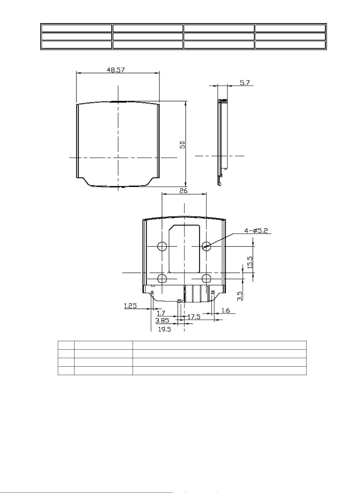
Dimension (W x H x L): 4.70 T x 35.70W x 47.05 L mm.
Weight: about 15.0 g.
*Operating times depend on network and usage. Variability will occur. DTX +40% (included).
Storage temperature:
Short period <1 month: -20°C to +45°C.
Long period <1 year: -20°C to +25°C.
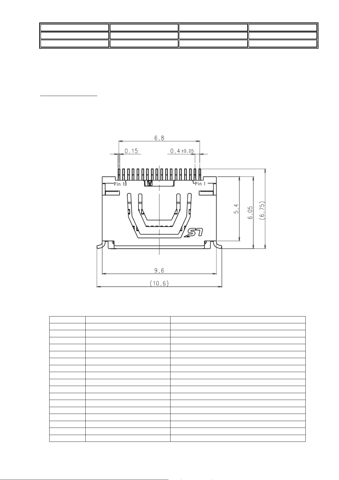
▪ I/O Connector layout : 18pin
Pin description
Pin 1
2
3
4
5
6
7
8
9
10
11
12
13
14
15
16
17
18
EJ_Out_L Headset Receiver Left
EJ_Out_R Headset Receiver Right
GND GND
EJ_Mic Headset Mic Input
GND GND
EJ_GND Headset GND
NC NC
Headset Interrupt Headset Interrupt
Power_On_Off Power On Off
USB_DM USB D+ input / Output
USB_DP USB D- input / Output
RXD UART RX
TXD UART TX
Charger/USB Power USB Power / Charger
Charger/USB Power USB Power / Charger
NC Not connected
VBAT Battery Voltage +3.8V
VBAT Battery Voltage +3.8V
Page 11

Model MASS 2 Version V_1.0
Prepared by H/W Date 22/01/2008
Subject Technical Manual Page 5/5
Standard charger
MASS 2 is supplied with a SMTP charger as standard. The charger is connected to the Power
management IC through the bottom port.
Charging of the battery can only be carried out when the battery is fitted to the phone. There are no
serviceable parts within the main plug.
Input parameter Type Value Unit
Input voltage min 90 V
nom 230 V
max 264 V
Input frequency min 47 Hz
nom 50 Hz
max 63 Hz
Input current max 200 mA
Efficiency min >55 %
Output parameter Type Value Unit
Output current(CV) min 0.650 A
max 0.800 A
(CC) min 0.000 A
max 0.650 A
Output voltage(CV) min 3.0 V
max 4.9 V
(CC) min 4.9 V
max 5.3 V
Connector 18pin Bottom Connector
Cable length 1.8 m.
Page 12
Model MASS 2 Version V_1.0
Prepared by H/W Date 22/01/2008
Subject Technical Manual Page 1/11
Disassembly
This section covers the assembly and disassembly of SLT100 phone. In order to carry out the
assembly or disassembly the following precautions should be taken:
1. A Plus screwdriver is required to remove the four retaining screws, which holds the two casings
together. Ensure that the screwdriver is narrow enough to reach the screws without causing
damage to the casing parts.
2. The phone should always be placed on a soft surface to minimise the risk of damage being
caused to the casing, window and keypad. If the PCB is to be removed, then care should be taken
not to stress or scratch the exposed LCD.
3. Observe anti-static precautions when handling the main PCB or any of its components.
4. Repairs carried out by unauthorised persons will result in the warranty on the unit becoming
void.
5. Do not use solvents to clean any of the casing parts or the LCD window.
Phone disassembly
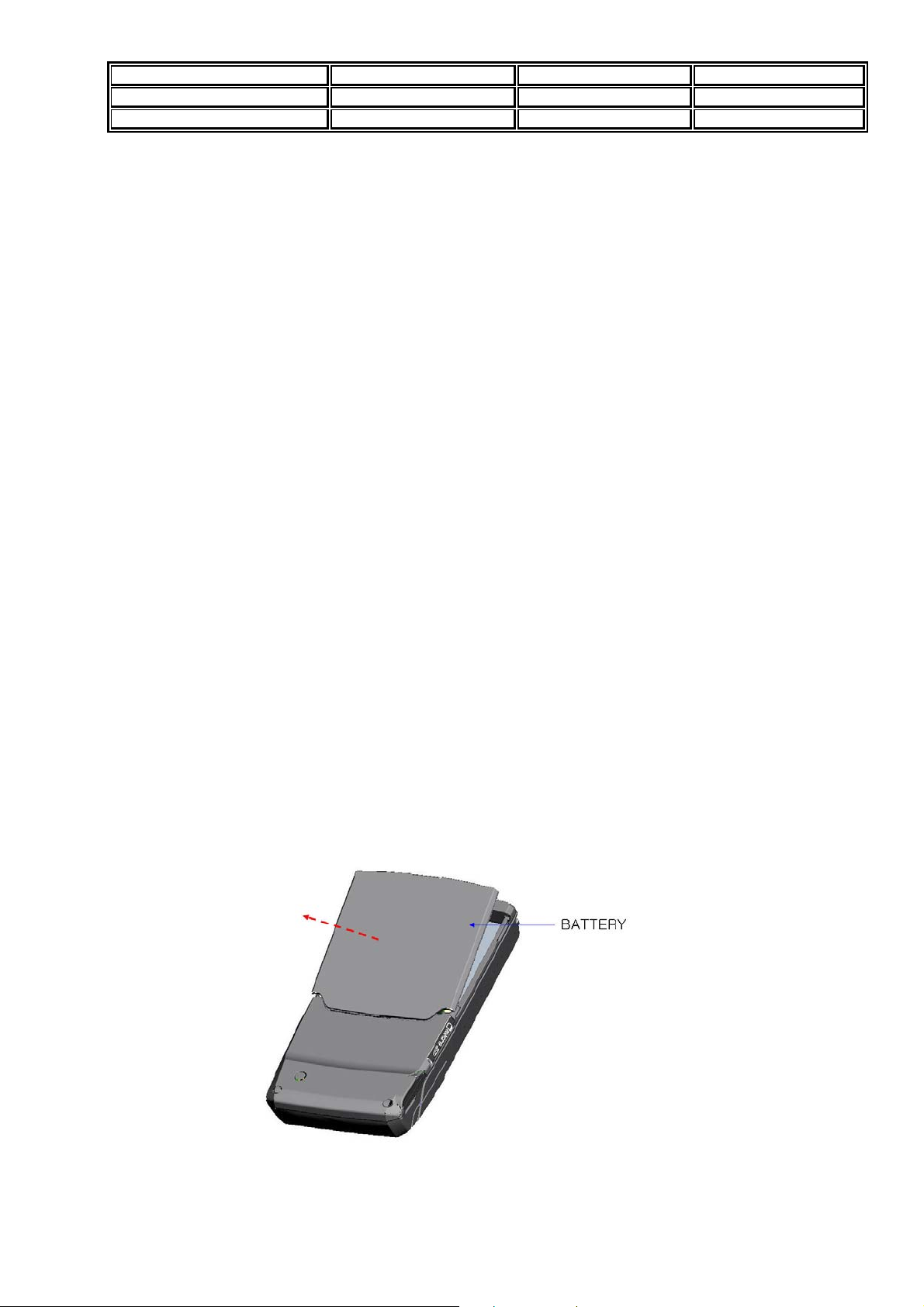
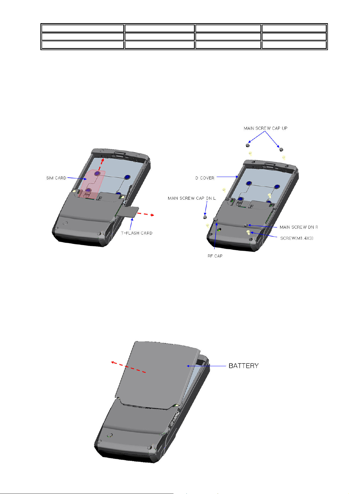
1. Battery Cover Disassembly
A. Shove battery cover out along the direction of arrow and remove battery cover.
B. Push up battery along the direction of arrow and remove battery.
Page 13
Model MASS 2 Version V_1.0
Prepared by H/W Date 22/01/2008
Subject Technical Manual Page 2/11
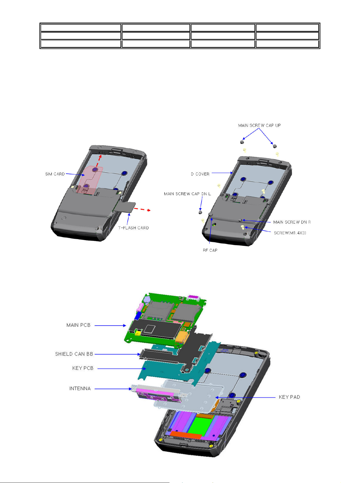
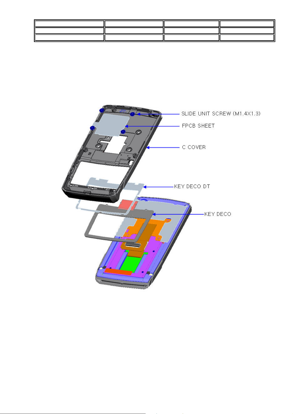
2. SIM card & TF card & caps & screws & D cover Disassembly
A. Remove SIM card
B. Remove TF card
C. Remove four caps and six screws. Carefully separate two covers
(C and D)
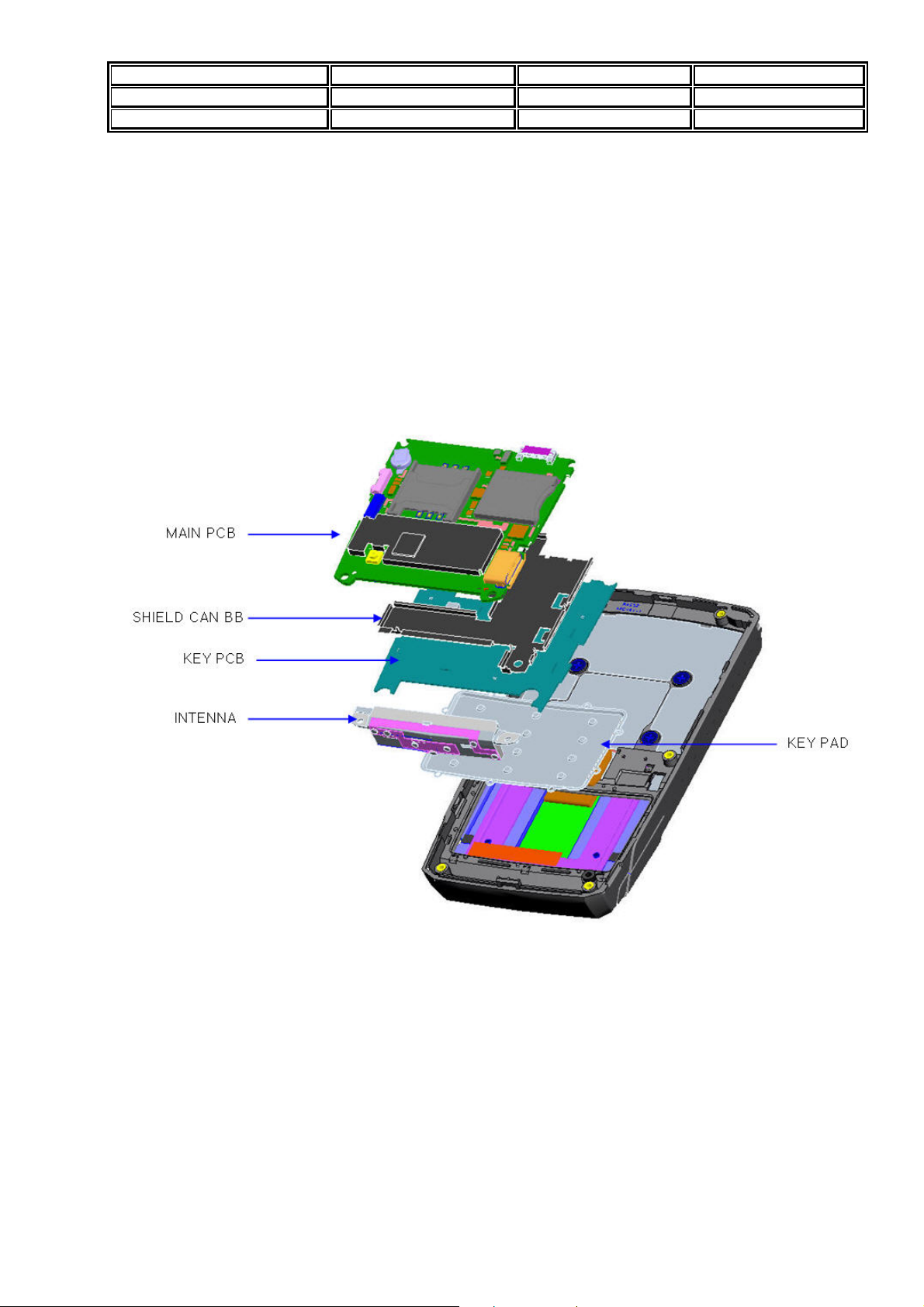
3. Main PCB & Main keypad & Cap IO Disassembly
Separate Main PCB manual ASS’Y and Main keypad ASS’Y from c cover.
Page 14
Model MASS 2 Version V_1.0
Prepared by H/W Date 22/01/2008
Subject Technical Manual Page 3/11
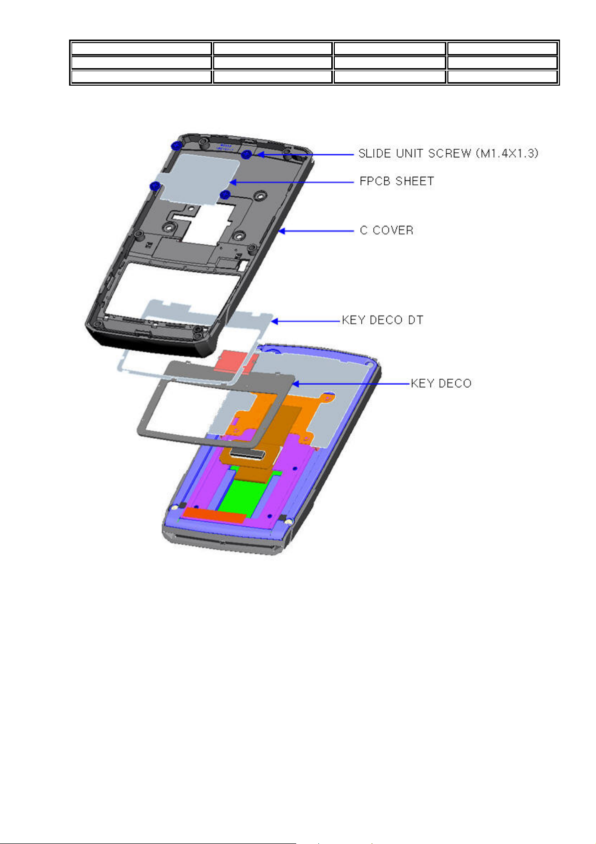
4. Front cover & Deco rail Disassembly
A. Unscrew four slide unit screws from c cover
B. Remove deco rail from front c cover.
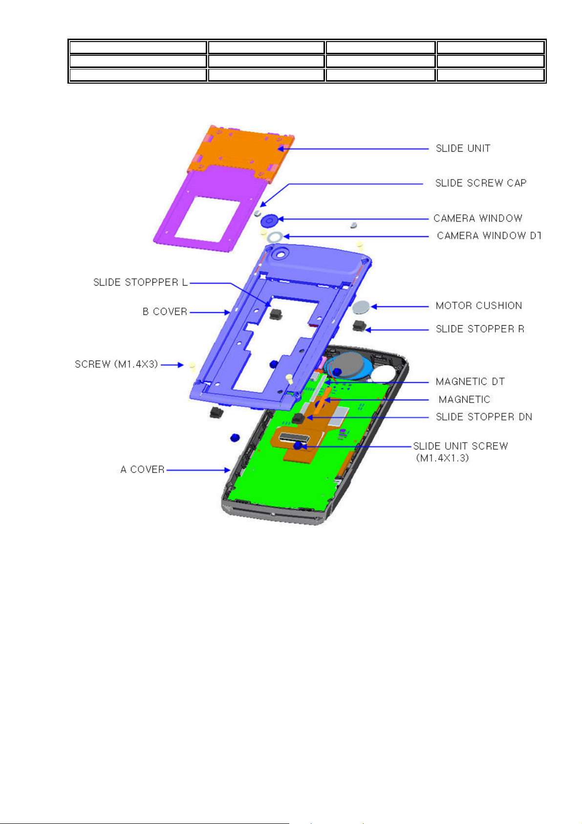
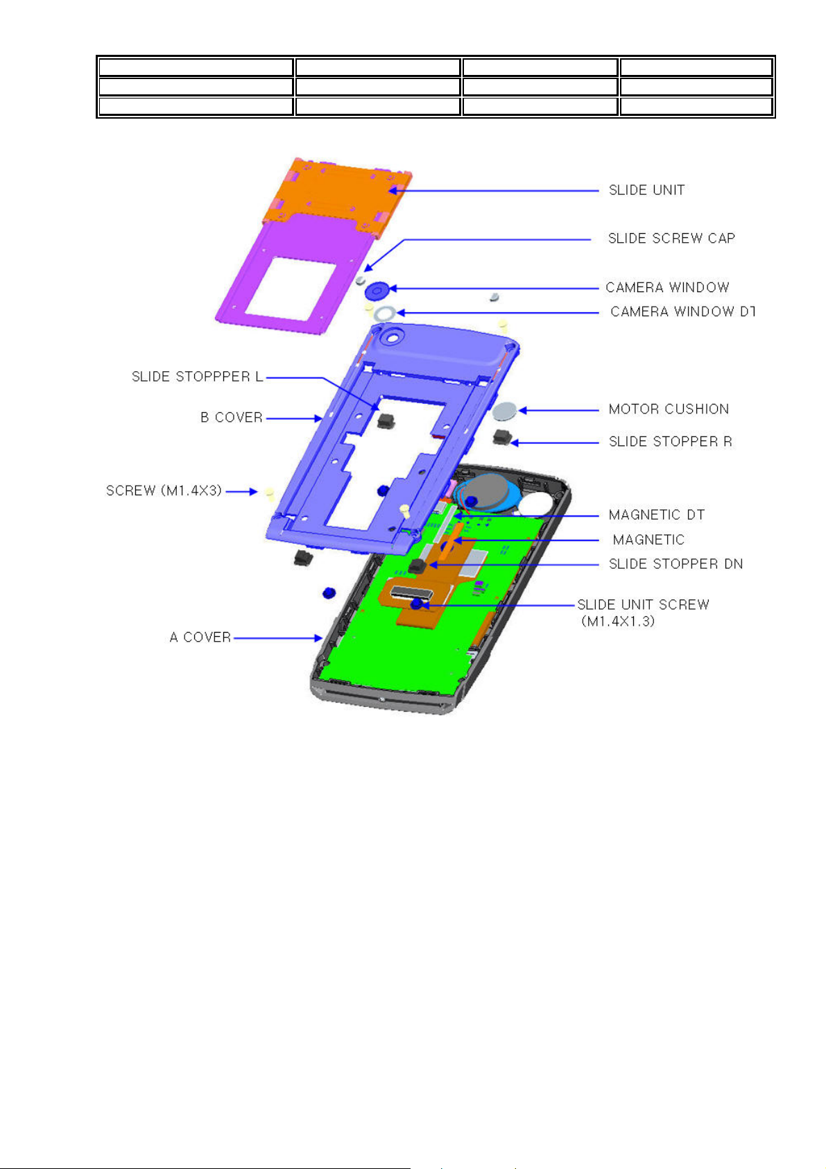
5. Slide unit & Stopper & B cover Disassembly
A. Remove two caps and four screws and carefully separate two covers
(A and B)
B. Unscrew six slide unit screws and remove slide unit
C. Remove slide unit
D. Pull off four stoppers from b cover
Page 15
Model MASS 2 Version V_1.0
Prepared by H/W Date 22/01/2008
Subject Technical Manual Page 4/11
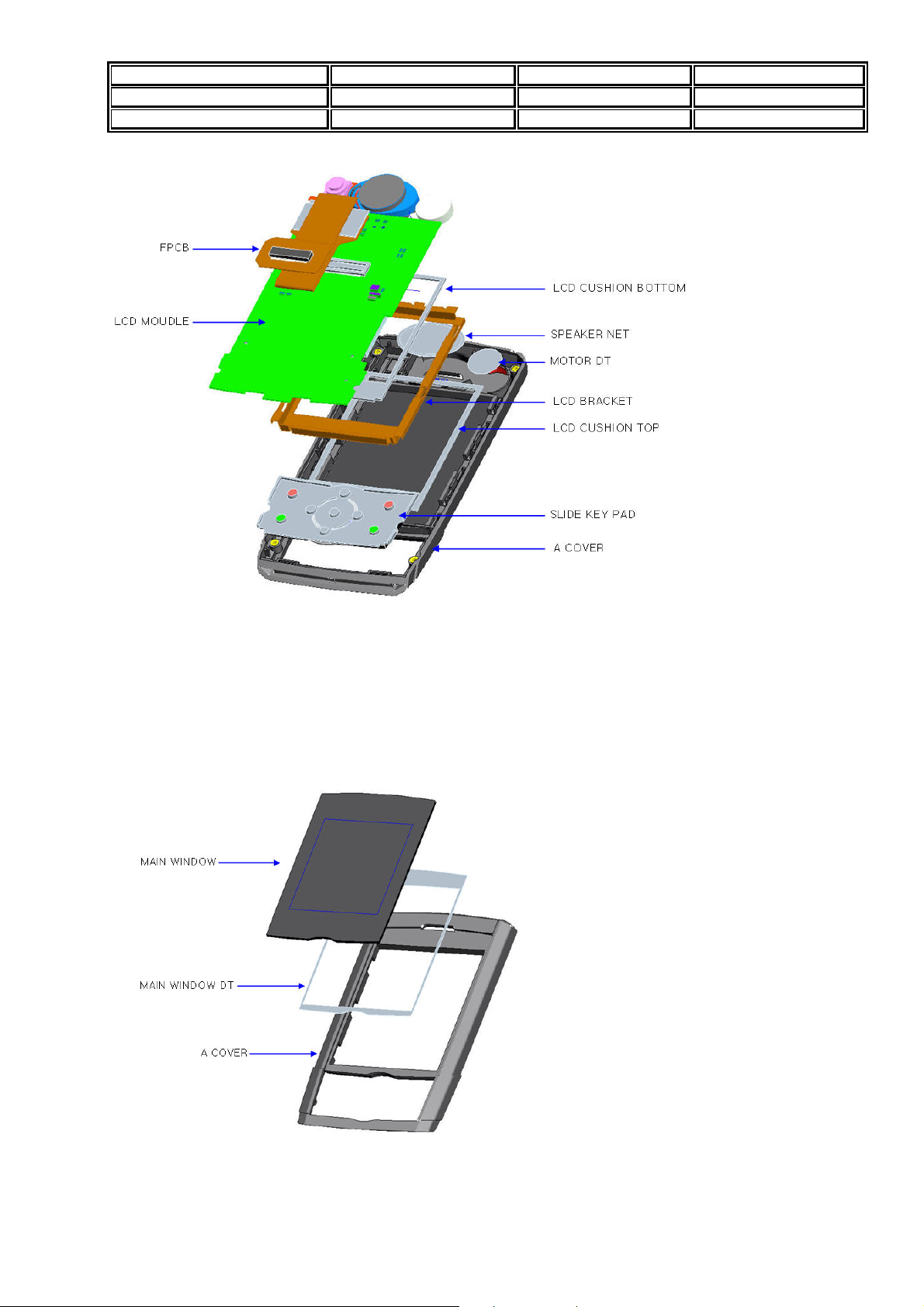
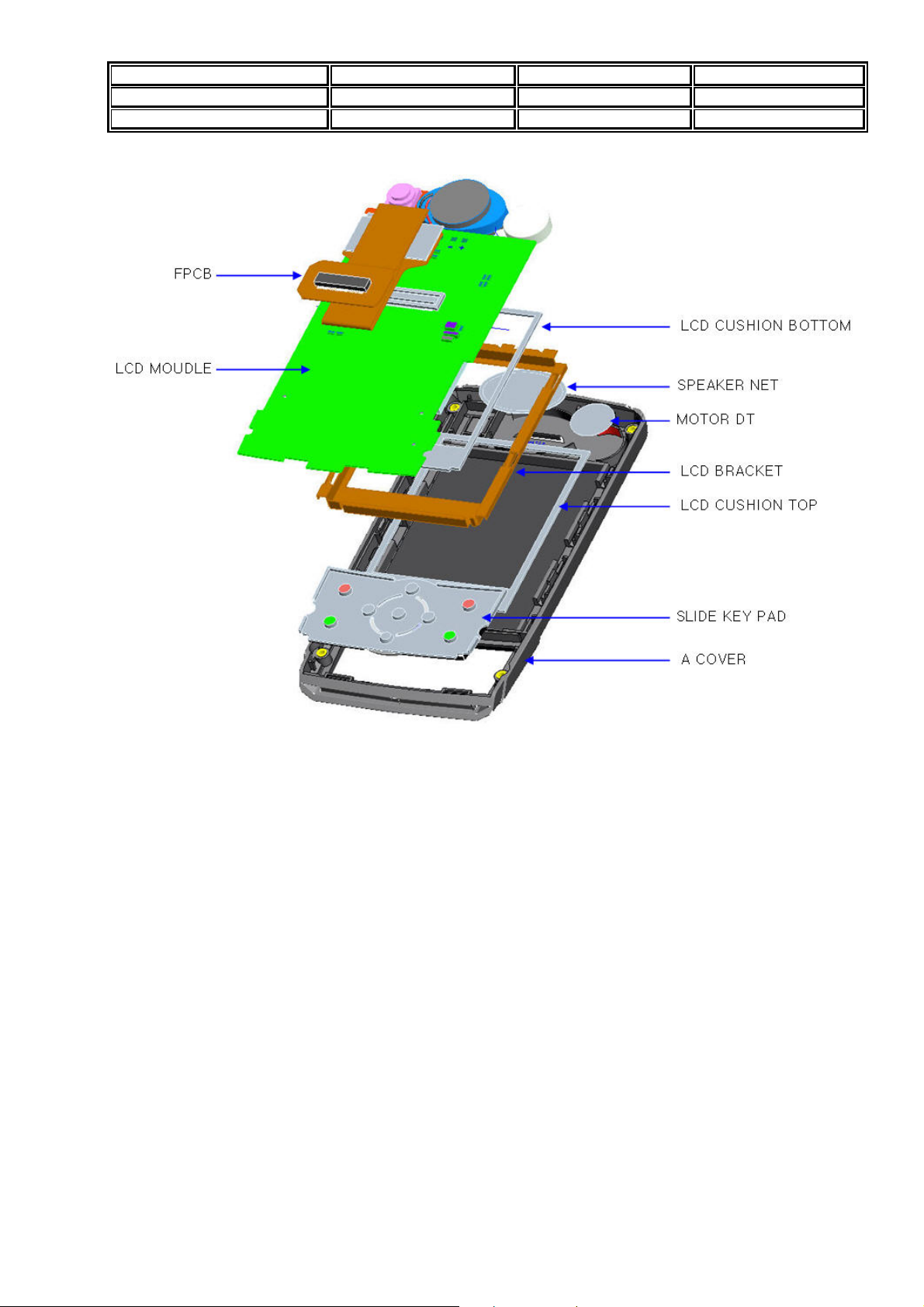
6. Lcd module & Keypad Disassembly
A. Remove LCD manual ASS’Y from a cover.
B. Remove keypad from a cover..
Page 16
Model MASS 2 Version V_1.0
Prepared by H/W Date 22/01/2008
Subject Technical Manual Page 5/11
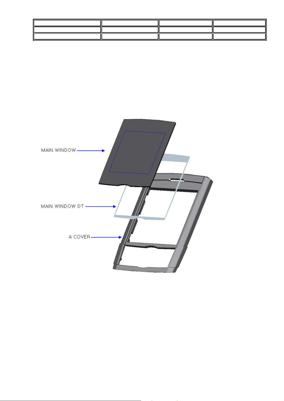
7. Main window Disassembly
A. Pull off main window from a cover.
Page 17
Model MASS 2 Version V_1.0
Prepared by H/W Date 22/01/2008
Subject Technical Manual Page 6/11
Phone Assembly
1. Top cover assembly
A. Attach the main window dt on the a cover
B. Attach the main window on the top cover.
2. LCD manual ASS’Y & slide keypad ASS’Y assembly
A. Group the slide keypad ASS’Y into the a cover.
B. Group the LCD bracket into the a cover
C. Group the LCD manual ASS’Y into the a cover
Page 18
Model MASS 2 Version V_1.0
Prepared by H/W Date 22/01/2008
Subject Technical Manual Page 7/11
3. Slide unit & Stopper & B cover assembly
A. Thrust four stoppers in stopper hole.
B. Assemble the magnetic in magnetic position.
C. Assemble the slide unit with b cover.
D. Screw up four slide unit screws.
E. Attach the D/T decoration back cover.
F. Carefully group the b cover
G. Screw up four screws
H. Attach the two cap screws
Page 19
Model MASS 2 Version V_1.0
Prepared by H/W Date 22/01/2008
Subject Technical Manual Page 8/11
4. C cover & Deco rail Assembly
A. Group the c cover with Deco rail.
B. Screw up four slide unit screws.
Page 20
Model MASS 2 Version V_1.0
Prepared by H/W Date 22/01/2008
Subject Technical Manual Page 9/11
Page 21
Model MASS 2 Version V_1.0
Prepared by H/W Date 22/01/2008
Subject Technical Manual Page 10/11
5. Main PCB & Main keypad Assembly
A. Group the main keypad ASS’Y, shield can bb, key pcb and main PCB manual ASS’Y
with c cover.
Page 22
Model MASS 2 Version V_1.0
Prepared by H/W Date 22/01/2008
Subject Technical Manual Page 11/11
8. Sim card & screw & caps & d cover Assembly
A. Assemble the d cover.
B. Screw up six screws and put in four caps.
C. Put the TF card and SIM card in.
9. Battery Assembly
B. Put the battery back cover on in the arrow direction.
.
Page 23
Model MASS 2 Version V_1.0
Prepared by H/W Date 22/01/2008
Subject Technical Manual Page 1/59
Baseband section
This document provides a description of the baseband section of the MASS 2. Most design decisions are explained,
but no detailed calculations are included. Total chip solutions(MT6225, MT6318, MT6120) except for RF Power
Amplifier(RF3166) are from MediaTek, Taiwan.
I. MT6225 ( GSM/GPRS Baseband Processor )
1. System OverView
The MT6225 is a highly integrated single-Chip solution for GSM/GPRS mobile phone. Based on 32bit ARM7EJ-STM
RISC processor, MT6225 features not only high performance GPRS Class 12 MODEM but is also designed with
support for the wireless multi-media applications. But, the MEGA2 just supports GPRS Multi-slot Class 8 and GPRS
MODE CLASS B.
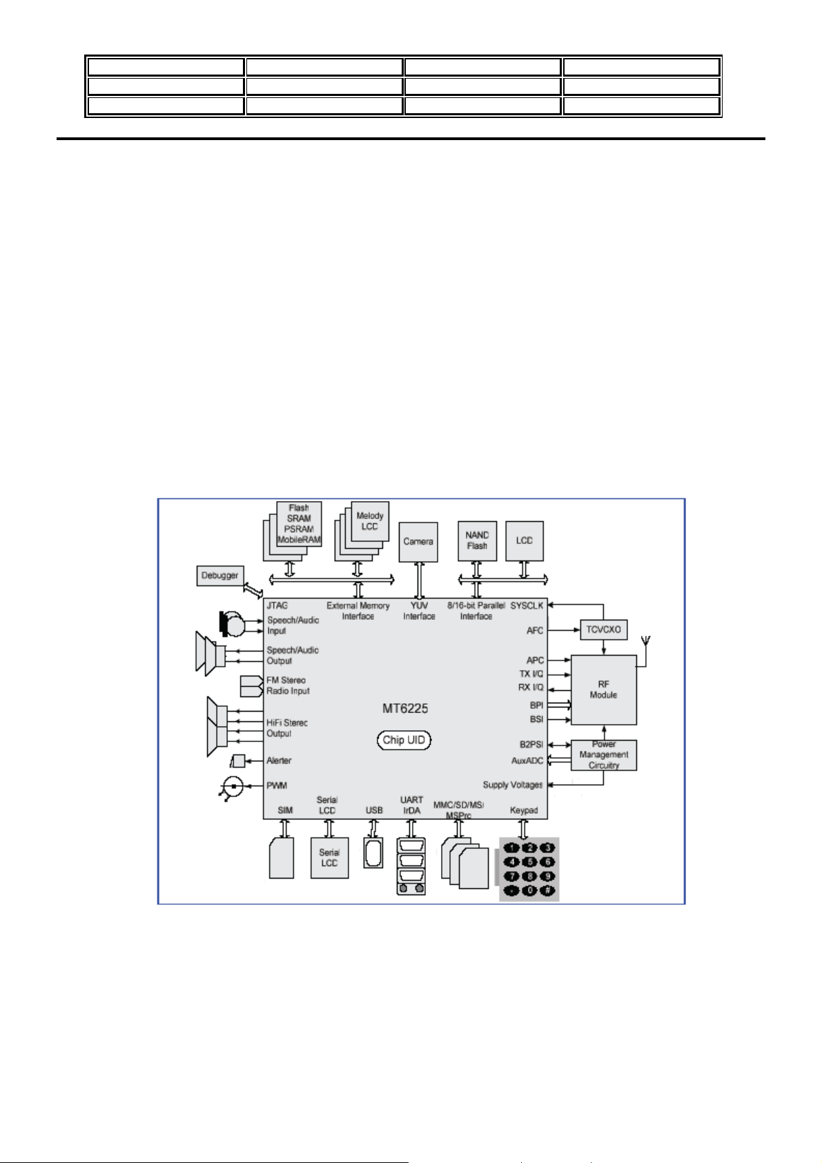
The Figure 1 is shown Typical Application for MT6225.
Figure 1 : Typical Application for MT6225
1.1 Platform Feature
z General
-. Integrated voice-band, audio-band and base-band analog front ends.
-. TFBGA 12mm x 12mm, 246-balls, 0.65mm pitch package.
z MCU Subsystem
Page 24

Model MASS 2 Version V_1.0
Prepared by H/W Date 22/01/2008
Subject Technical Manual Page 2/59
-. ARM7EJ-S 32bit RISC processor
-. High Performance Multi-layer AMBA bus
-. Java hardware acceleration for fast Java-based games and applets.
-.Operating frequency : 25/52/104Mhz
-. Dedicated DMA Bus
-. 14 DMA channels
-. 48K Bytes on-chip SRAM
-. 72K Bytes MCU dedicated Tightly Coupled memory
-. 16K Bytes CODE cache
-. On-chip boot ROM for factory flash programming
-. Watchdog timer for system crash recovery
-. 2sets of General purpose timer
-. Circuit Switch Data coprocessor
-. Division coprocessor.
z External Memory Interface
-. Supports up to 3 external devices
-. Supports 8-bit or 16-bit memory components with maximum size of up to 64M bytes each.
-. Supports Mobile RAM and Cellular RAM
-. Supports Flash and SRAM/PSRAM with page mode or burst mode
-. Supports Pseudo SRAM
-. Industry standard Parallel LCD interface
-. Supports Multi-media companion chips with 8/16bits data width.
-. Flexible I/O voltage of 1.8V ~ 2.8V for memory interface.
z User Interface
-. 6-row x 7-column keypad controller with hardware scanner.
-. Supports multiple key presses for gaming.
-. SIM/USIM controller with hardware T=0/T=1 protocol control.
-. Real Time Clock(RTC) operating with a separate power supply.
-. General Purpose I/Os (GPIOs)
-. 2sets of Pulse Width Modulation(PWM) output.
-. Alerter Output with enhanced PWM or PDM.
-. 4 ~ 10 external interrupt lines.
z Security
-. Supports security key for code protection
-. 143-bit unique/secret chip ID
z Connectivity
-. 3 UARTs with hardware flow control and speed up to 921600pbs.
-. IrDA modulator/Demodulator with hardware framer. Supports SIR/MIR/FIR operating Speeds.
-. Full speed USB 1.1 Device controller
Page 25

Model MASS 2 Version V_1.0
Prepared by H/W Date 22/01/2008
Subject Technical Manual Page 3/59
-. Multi Media Card, Secure Digital Memory Card, Memory Stick, Memory Stick Pro Host Controller
-. Supports SDIO interface for SDIO peripherals as well as WIFI connectivity.
-. DAI/PCM and I2S interface for Audio application.
z Power Management
-. Power Down Mode for analog and digital circuits.
-. Processor Sleep Mode
-. Pause Mode of 32Khz clocking in Standby state
-. 7 channel Auxiliary 10bit A/D converter for charger and battery monitoring and photo sensing.
z Test and Debug
-. Built-in digital and analog loop back modes for both Audio and baseband front-end.
-. DAI port complying with GSM Rec.11.10
-. JTAG port for debugging embedded MCU.
1.2 Model Feature
z Radio Interface and Baseband Front End
-. GMSK Modulator with analog I and Q channel outputs.
-. 10-bit D/A convert for Uplink baseband I and Q signals.
-. 14bit high resolution A/D converter for downlink baseband I and Q signals.
-. Calibration mechanism of offset and gain mismatch for baseband A/D converter and D/A converter.
-. 10bit D/A converter for Automatic Power Control(APC)
-. 13bit high resolution D/A converter for Automatic frequency Control(AFC)
-. Programmable Radio RX filter.
-. 2 channels Baseband Serial Interface(BSI) with 3-wire control.
-. 10 pin Baseband Parallel Interface(BPI) with programmable driving strength.
-.Multi-band Support (GSM850, GSM900, DCS1800, PCS1900)
z Voice and Model Codec
-. Dial tone Generation.
-. Voice memo
-. Noise reduction
-. Echo suppression
-. Advanced sidetone Oscillation Reduction.
-. Digital sidetone generator with programmable gain.
-.Two programmable acoustic compensation filters.
-. GSM/GPRS quad vocoders for adaptive multirate(AMR), enhanced full rate(EFR), full rate(FR) and half rate(HR).
-. FR error concealment
-. GSM channel coding, equalization and A5/1, A5/2 and A5/3 ciphering
-.GPRS GEA1, GEA2 and GEA3 ciphering.
-. Programmable GSM/GPRS modem
-. Packet Switched data with CS1/CS2/CS3/CS4 coding schemes.
-.GSM circuit switch data.
Page 26

Model MASS 2 Version V_1.0
Prepared by H/W Date 22/01/2008
Subject Technical Manual Page 4/59
-. GPRS Class 12.
z Voice Interface and Voice Front End.
-. Two microphone inputs sharing one low noise amplifier with programmable gain and automatic gain control(AGC)
mechanisms.
-. Voice power amplifier with programmable gain.
-. 2’nd order Sigma-Delta A/D converter for voice uplink path.
-. D/A Converter for Voice downlink path.
-. Supports Half-duplex hands-free operation.
-. Compliant with GSM 03.50.
1.3 Multimedia Feature
z LCD/NAND Flash Interface
-. 18-bit Parallel Interface supports 8/16 bit NAND flash and 8/9/16/18 bit Parallel LCD
-. 8/16 bit NAND Flash Controller with 1-bit ECC correction for mass storages
-. 2 Chip selects available for high – density NAND flash device
z LCD Controller
-. Supports simultaneous connection to up to 2 parallel LCD and 1 serial LCD modules.
-. Supports LCM format : RGB332, RGB444, RGB565, RGB666, RGB888.
-. Supports LCD Module with maximum resolution up to 800x600 at 16bpp.
-. Supports hardware display rotation
-. Accelerated Gamma correction with programmable table.
-. Capable of combining display memories with up to 4 blending layers.
z Image Signal Processor
-. 8 bit YUV format image input.
-. Capable of processing image of size up to VGA
-. Flexible I/O voltage of 1.8V ~ 2.8V
-. RGB thumbnail data output.
z Audio CODEC
-. Wavetable synthesis with up to 64 tones
-. Advanced wavetable synthesizer capable of generating simulated stereo
-. Wavetable including GM full set of 128 instruments and 47 sets of percussions
-. PCM Playback and Record
-. Digital Audio Playback
-. HE – ACC decode support
z Audio Interface and Audio Front End
-. Supports I2S interface
-. High resolution D/A Converters for Stereo Audio playback
-. Stereo analog input for stereo audio source
-. Analog multiplexer for stereo audio
-. Stereo to mono conversion
Page 27
Model MASS 2 Version V_1.0
Prepared by H/W Date 22/01/2008
Subject Technical Manual Page 5/59
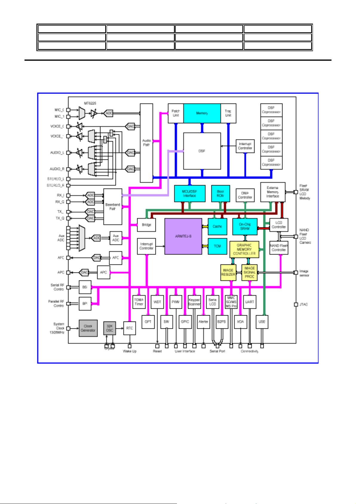
Figure 2 is shown the Block Diagram of MT6225 for detailed.
Figure 2 : Block Diagram of MT6225
2. Product Description
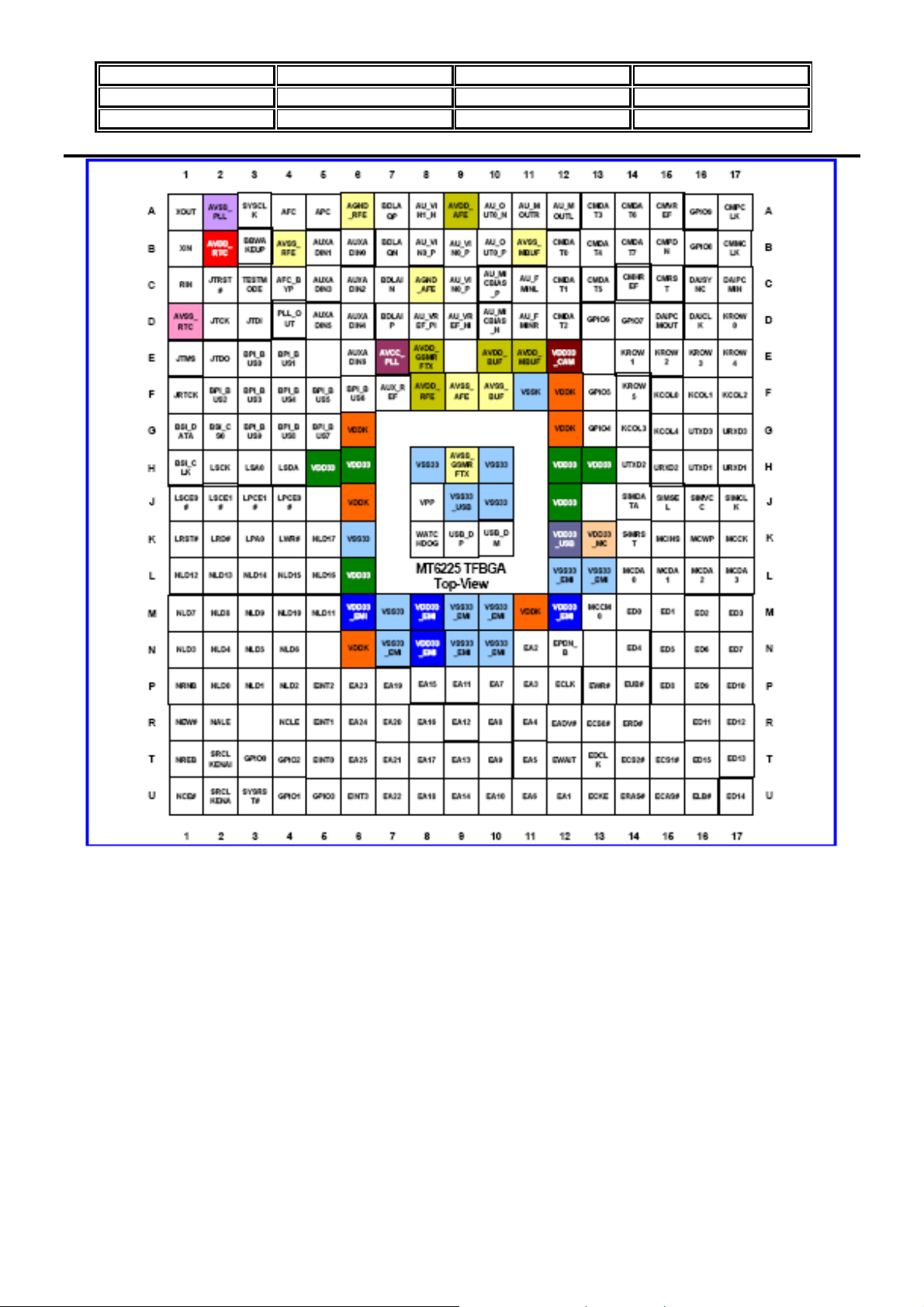
Pin Outs
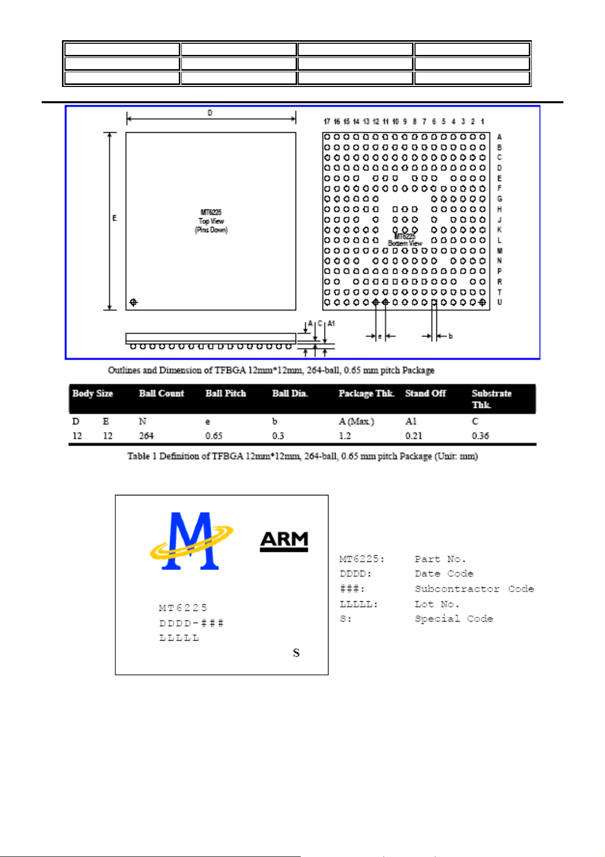
One type of Package for this product, TFBGA 12x12mm, 264 balls, 0.65mm pitch package, is offered.
Pin outs and the top view are illustrated in Figure 3
-. Pin Out
Page 28
Model MASS 2 Version V_1.0
Prepared by H/W Date 22/01/2008
Subject Technical Manual Page 6/59
-. Top and Bottom View
Figure 3 . MT6225 Pin Out.
Page 29
Model MASS 2 Version V_1.0
Prepared by H/W Date 22/01/2008
Subject Technical Manual Page 7/59
Top Masking Definition
Figure 5. Top masking definition
Page 30
Model MASS 2 Version V_1.0
Prepared by H/W Date 22/01/2008
Subject Technical Manual Page 8/59
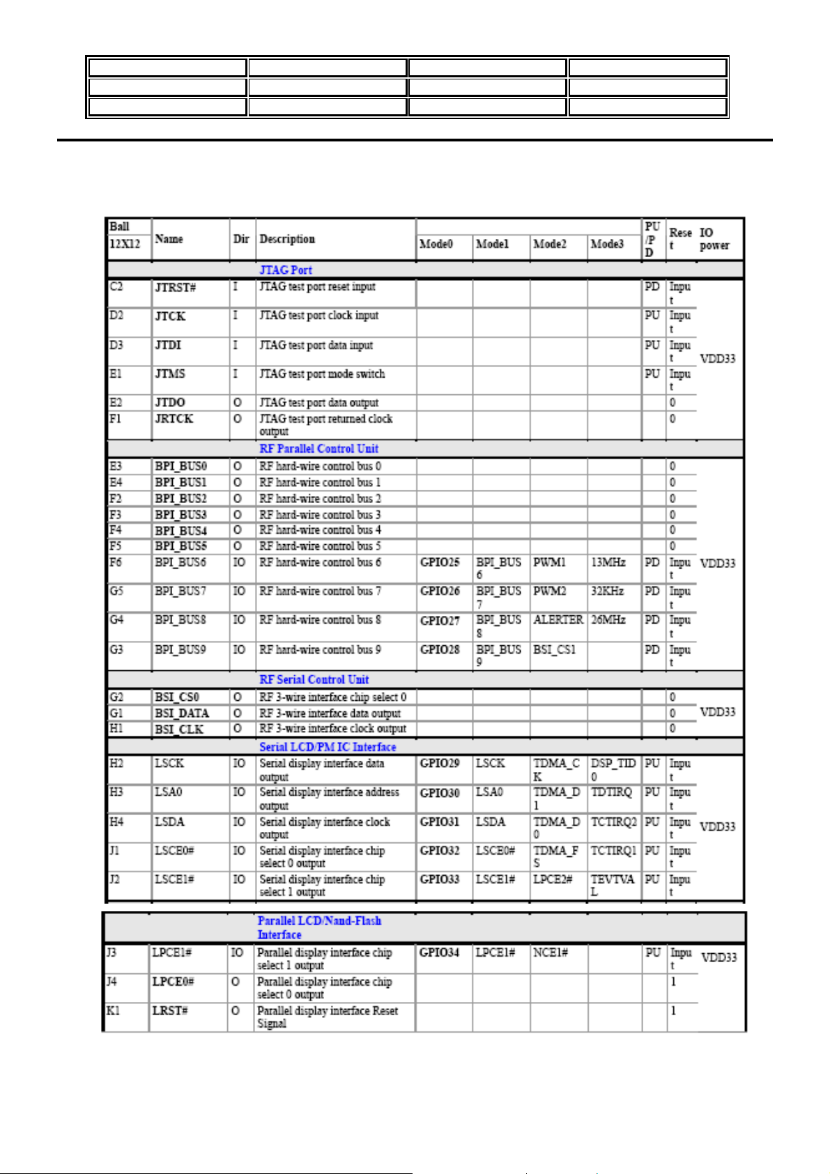
Pin Description
Page 31

Model MASS 2 Version V_1.0
Prepared by H/W Date 22/01/2008
Subject Technical Manual Page 9/59
Page 32

Model MASS 2 Version V_1.0
Prepared by H/W Date 22/01/2008
Subject Technical Manual Page 10/59
Page 33

Model MASS 2 Version V_1.0
Prepared by H/W Date 22/01/2008
Subject Technical Manual Page 11/59
Page 34

Model MASS 2 Version V_1.0
Prepared by H/W Date 22/01/2008
Subject Technical Manual Page 12/59
Page 35

Model MASS 2 Version V_1.0
Prepared by H/W Date 22/01/2008
Subject Technical Manual Page 13/59
Page 36

Model MASS 2 Version V_1.0
Prepared by H/W Date 22/01/2008
Subject Technical Manual Page 14/59
Page 37

Model MASS 2 Version V_1.0
Prepared by H/W Date 22/01/2008
Subject Technical Manual Page 15/59
Page 38

Model MASS 2 Version V_1.0
Prepared by H/W Date 22/01/2008
Subject Technical Manual Page 16/59
3. Micro-Controller Unit Subsystem
Figure 6 illustrates the block diagram of the Micro-Controller Unit Subsystem in MT6225. The Subsystem utilizes a
main 32-bit ARM7EJ-S RISC processor, which plays the role of the main bus master controlling the whole subsystem.
All processor transactions go to code cache first. The code cache controller accesses TCM(72KB memory dedicated to
ARM7EJS core), cache memory, or bus according to the processor’s request address, If the requested content is found in
TCM or in cache, no bus transaction is required. If the code cache hit rate is high enough, bus traffic can be effectively
reduced and processor core performance maximized. In addition to the benefits of reuse of memory contents, code cache
also has a MPU(Memory Protection Unit), which allows cacheable and protection settings of predefined regions. The
contents of code cache are only accessible to MCU, and only MCU instructions are kept in the cache memory.
The MT6228 MCU subsystem supports only memory addressing method. Therefore all components are mapped onto the
MCU 32-bit address space. A Memory Management Unit is employed to allow for a central decode scheme.
The MMU generates appropriate selection signals for each memory-addressed module on the AHB Bus.
External Memory Interface supports both 8-bit and 16-bit devices. Since AHB Bus is 32-bit wide, all the data transfer
Will be converted into several 8-bit or 16-bit cycles depending on the data width of target device. Note that, this interface
is specific to both synchronous and asynchronous components, like Flash, SRAM and parallel LCD. This interface
supports also page and burst mode type of Flash.
Figure 6. Block Diagram of MCU in MT6225
Page 39

Model MASS 2 Version V_1.0
Prepared by H/W Date 22/01/2008
Subject Technical Manual Page 17/59
3.1 Processor Core
The Micro-Controller Unit subsystem in MT6225 is built up with a 32-bit RISC core, ARM7EJ-S that is based on the
Von Neumann architecture with a single 32-bit data bus carrying both instructions and data. The memory interface of
ARM7EJ-S is totally compliant to AMBA based bus system. Basically, it can be connected to AHB Bus directly.
3.2 Memory Management
The processor core of MT6225, ARM7EJ-S, supports only memory addressing method for instruction fetch and data
access. It manages a 32bit address space that has addressing capability up to 4GB. System RAM, System ROM ,
Registers, MCU Peripherals and external components are all mapped onto such 32-bit address space, as depicted in
Figure 7.
Figure 7. Memory Layout of MT6225
External Memory Access
To allow external access, the MT6225 outputs 25 bits (A25-A1) of address lines along with 4 selection signals that
correspond to associated memory blocks. That is, MT6225 can support up to 3 MCU addressable external components.
The data width of internal system bus is fixed at 32-bit wide, while the data width of the external components is fixed as
16 bit.
Factory Programming
The configuration for factory programming is shown in Figure 8. Usually the Factory Programming Host connects
with MT6225 via the UART interface. The download speed can be up to 921K bps while MCU is running at 26MHz.
Page 40

Model MASS 2 Version V_1.0
Prepared by H/W Date 22/01/2008
Subject Technical Manual Page 18/59
After the system has reset, the Boot Code guides the processor to run the Factory Programming software placed in
System ROM. Then, MT6225 starts and polls the UART1 port until valid information is detected. The first information
received on the UART1 is used to configure the chip for factory programming. The Flash downloader program is then
transferred into System RAM or external SRAM. Further information is detailed in the MT6228 Software Programming
Specification.
Figure 8. Factory Programming
3.3 Interrupt Controller
Figure 10 outlines the major functionality of the MCU Interrupt Controller. The interrupt controller processes all
interrupt sources coming from external lines and internal MCU peripherals. Since ARM7EJ-S core supports two levels
of interrupt latency, this controller generates two request signals: FIQ for fast, low latency interrupt request and IRQ for
more general interrupts with lower priority.
Figure 10. Block Diagram of Interrupt controller.
Page 41

Model MASS 2 Version V_1.0
Prepared by H/W Date 22/01/2008
Subject Technical Manual Page 19/59
External Interrupt
This interrupt controller also integrates an External Interrupt Controller that can support up to 4 interrupt tequests
Coming from external sources, the EIMT 0 ~ 3, and 4 WakeUp interrupt requests, i.e. EINT4~7, coming from
peripherals used to inform system to resume the system clock..
Block diagram of external interrupt controller .
3.4 Internal Memory Interface
System Ram
MT6225 provides one 72 KByte size of on-chip memory modules acting as System RAM for data access with low latency.
Such a module is composed of one high speed synchronous SRAMs with AHB Slave Interface connected to the system
backbone AHB Bus, The synchronous SRAM operates on the same clock as the AHB Bus and is organized as 32 bits wide
with 4 byte-write signals capable for byte operations. The SRAM macro has limited repair capability. The yield of SRAM is
improved if the defects inside it can be repaired during testing.
System ROM
The 15K Bytes System ROM is primarily used to store software program for Factory Programming. This module is
composed of high-speed ROM with an AHB Slave Interface connected to a system backbone AHB. The module operates on
the same clock as the AHB and has a 32-bit wide organization.
3.5 External Memory Interface
MT6228 incorporates a powerful and flexible memory controller, External Memory Interface, to connect with a variety of
memory components. This controller provides one generic access scheme for Flash Memory, SRAM, PSRAM and
CellularRAM and another access scheme for MobileRAM. Up to 3 memory banks can be supported simultaneously, BANK0BANK2, with a maximum size of 64MB each. Since most of the Flash Memory, SRAM, PSRAM and CellularRAM have
Page 42

Model MASS 2 Version V_1.0
Prepared by H/W Date 22/01/2008
Subject Technical Manual Page 20/59
similar AC requirements, a generic configuration scheme to interface them is desired. This way, the software program can
treat different components by simply specifying certain predefined parameters. All these parameters are based on the cycle
time of system clock. The interface definition based on such a scheme is listed in Table 17. Note that, this interface always
works with data in Little Endian format for all types of access.
Table 17 External Memory Interface Signal of MT6225
4. Microcontroller Peripherals
Microcontroller(MCU) Peripherals are devices that are under direct control of the Microcontroller. Most of the devices are
attached to the Advanced Peripheral Bus(APB) of the MCU subsystem, and serve as APB slaves. Each MCU peripheral must
be accessed as a memory-mapped I/O device: that is, the MCU or the DMA bus master reads from or writes to the specific
peripheral by issuing memory-addressed transactions.
Pulse-Width Modulation Outputs.
Two generic Pulse-Width Modulators are implemented to generate pulse sequences with programmable frequency and duty
cycle for LCD backlight or charging purpose. The duration of the PWM output signal is low as long as the internal counter
value is greater than or equal to the threshold value.
SIM Interface
The MT6225 contains a dedicated smart card interface to allow the MCU access to the SIM card. It can operate via 5
terminals, using SIMVCC, SIMSEL, SIMRST, SIMCLK and SIMDATA.
The SIMVCC is used to control the external voltage supply to the SIM card and SIMSEL determines the regulated smart card
supply voltage. SIMRST is used as the SIM card reset signal. Besides, SIMDATA and SIMCLK are used for data exchange
purpose. Basically, the SIM interface acts as a half duplex asynchronous communication port and its data format is composed
of ten consecutive bits: a start bit in state Low, eight information bits and a tenth bit used for parity checking.
Page 43

Model MASS 2 Version V_1.0
Prepared by H/W Date 22/01/2008
Subject Technical Manual Page 21/59
Figure 12. SIM interface
Figure 13. SIM/TFLASH Connector Circuit of MASS 2
In MEGA2, The SIM Connector is soldered on FPCB with T-Flash Connector as above Figure 13.
Keypad Scanner
The keypad can be divided into two parts : One is the keypad interface including 7 columns and 6 rows The other is the key
detection block which provides key pressed, key released and de-bounce mechanism. Each time the key is pressed or released,
i.e. something different in the 7x6 matrix, the key detection block will sense it, and it will start to recognize if it is a key
pressed or key released event. Whenever the key status changes and is stable, a KEYPAD IRQ will be issued. The MCU can
then read the key pressed directly in KP_HI_KEY, KP_MID_KEY and KP_LOW_KEY register.
In MASS 2, The 5 Rows are used (Row0 ~Row4) and The 5 Columns are used (Col 0~4)
Figure 14. Key pressed with de-bounce mechanism
Page 44

Model MASS 2 Version V_1.0
Prepared by H/W Date 22/01/2008
Subject Technical Manual Page 22/59
In MASS2, The 5 Rows are used (Row0 ~Row4) and The 5 Columns are used (Col 0~4)
The 3x4 and Power On Keys are on Main Body. And Soft_Left/Right, Navy key are on LCD Body.
The Figure 15 shows the circuit.
Figure 15. MASS 2 Key Scan Circuit.
General Purpose Inputs/Outputs
MT6225 offers 53 general purpose I/O pins and 4 general-purpose output pins. By setting the control registers, MCU software
can control the direction, the output value and read the input values on these pins. These GPIOs and GPOs are multiplexed
with other functionalities to reduce the pin count.
Upon hardware reset(/SYSRST), GPIOs are all configured as inputs and the following alternate usages of the GPIO pins are
enabled.
Multiplexing of Signals on GPIO
The GPIO pins can be multiplexed with other signals.
-. DAICLK, DAIPCMIN, DAIPCMOUT, DAIRST: digital audio interface for FTA
-. BPI_BUS6, BPI_BUS7, BPI_BUS8, BPI_BUS9: radio hardwired control
-. BSI_CS1: additional chip select signal for radio 3-wire interface
-. LSCK, LSA0, LSDA, LSCE0#, LSCE1#: serial display interface
-. LPCE1#: parallel display interface chip select signal
-. NRNB, NCLE, NALE, NWEB, NREB, NCEB: NAND flash control signals
-. PWM1, PWM2: pulse width modulation signal ALERTER: pulse width modulation signal for buzzer
-. IRDA_RXD, IRDA_TXD, IRDA_PDN: IrDA control signals
-. URXD2, UTXD2, UCTS2, URTS2: data and flow control signals for UART2
-. URXD3, UTXD3, UCTS3, URTS3: data and flow control signals for UART3
Page 45

Model MASS 2 Version V_1.0
Prepared by H/W Date 22/01/2008
Subject Technical Manual Page 23/59
-. CMRST, CMPDN, CMDAT7 ~ CMDAT0: sensor interface
Multiplexed of Signals on GPO
-. SRCLKENA, SRCLKENAN: power on signal of the external VCXO LDO
-. EA25, EA24 : external memory interface address bit[25:24]
-. EPDN_B: external memory interface power down controls
-. 32KHz, 6.5MHz, 13MHz, 26MHz clocks
UART
The baseband chipset houses three UARTs. The UARTs provide full duplex serial communication channels between
baseband chipset and external devices. The UART has M16C450 and M16550A modes of operation, which are compatible
with a range of standard software drivers.
In MASS2, UART1(URXD1, UTXD1) is used for Factory Programming and UART3(URXD3, UTXD3) is used for Blue
Tooth Programming.
Figure 16. UART block diagram.
RX data Timeout Interrupt :
When virtual FIFO mode is disabled, RX data Timeout Interrupt is generated if all of the following apply :
1. FIFO contains at least on character.
2. The most recent character was received longer than four character periods ago(including all start, parity and stop bit)
3. The most recent CPU read of the FIFO was longer than four character periods ago.
When virtual FIFO mode is enabled, RX Data timeout Interrupt is generated if all of the following apply:
1. FIFO is empty.
2. The most recent character was received longer than four character periods ago(including all start, parity and stop bit)
3. The most recent CPU read of the FIFO was longer than four character periods ago
IrDA : Available
MASS2 uses the HSDL-3208 IrDA Module. The HSDL-3208 is an ultra-small low cost infrared transceiver module that
provides the interface between logic and infrared(IR) signals for through air, serial, half duplex IR data link. The Module is
Page 46

Model MASS 2 Version V_1.0
Prepared by H/W Date 22/01/2008
Subject Technical Manual Page 24/59
compliant to IrDA physical layer specifications version 1.4 Low Power from 9.6kbit/s to 115.2kbit/s with extended link
distance and it is IEC 825-Class 1 eye safe. .
Window material : Almost any plastic material will work as a window material. Polycarbonate is recommended. The surface
finish of the plastic should be smooth, without any texture.
Shape of the Window : From an optics standpoint, the window should be flat. This ensures that the window will not alter
either the radiation pattern of the LED, or the receive pattern of the photo diode. If the window must be curved for mechanical
or industrial design reasons, place the same curve on the back side of the window that has an identical radius as the front side
Selection of Resistor R1Resistor : R1 should be selected to provide the appropriate peak pulse LED current over different
ranges of VCC 3.3V and Minimum Peak Pulse Current 50mA.
Figure 17. IrDA Block Diagram. Figure 18. IrDA Circuit.
Read Time Clock
The Real Time Clock (RTC) module provides time and data information. The clock is based on a 32.768Khz oscillator with
an independent power supply. When the mobile handset is powered off, a dedicated regulator supplies the RTC block. If the
main battery is not present, a backup supply such as a small mercury cell battery or a large capacitor is used. In addition to
providing timing data, an alarm interrupt is generated and can be used to power up the baseband core via the BBWAKEUP pin.
Regulator interrupts corresponding to seconds, minutes, hours and days can be generated whenever the time counter value
reaches a maximum value. The Maximum day-of-month values, which depend on the leap year condition, are stored in the
RTC block.
In MASS2, Big Capacitor Battery(BAT300 SF-3R3-S104Z) is used for Backup Battery. The Charging Voltage is about 1.5V
by VRTC. The ST4115 is a Cristal for 32.768Khz and The C126,C127 must be tuned.
Page 47

Model MASS 2 Version V_1.0
Prepared by H/W Date 22/01/2008
Subject Technical Manual Page 25/59
Figure 19. RTC Circuit
Auxiliary ADC Unit
The auxiliary ADC unit is used to monitor the status of battery and charger, identify the plugged peripheral and perform
temperature measurement. There provides 7 input channels for diversified application in this unit.
In MASS 2, 6 ADC port are used as shown Figure 20.
Figure 20. AUXADC Circuit
1) ADC0/1_I-/+ : Check the Battery and Charger voltage.
2) ADC2_TBAT : Connected to battery ID Resistor. Check the Battery Temperature by NTC ID Resistor(10Kohm),
So, the voltage is about 0.6V in normal temperature.
3) ADC3_VCHG : Check and detect the the charger. If charger is connected the Voltage is changed from 0V to 1V.
So, MT6228 can know the charger inserted.
4) ADC4_USB : Check and detect the USB cable. If USB cable is inserted, voltage of ADC4_USB pin is changed
from 2.8V to 0V (2.8V Æ Pulse Æ 0V). So, MT6228 can know the USB cable inserted.
5) ADC5_HF_MIC : Check and Detect the Headset(Ear Microphone). If Ear microphone is inserted, the voltage of
ADC5_HF_MIC is changed from 2.8V to about 1.5V(1.2~1.8V. depending on CMIC resistance).
6) ADC6_REMOTE : Check and operating the remote control headset(MP3 Remote Control Headset)
5. Multi-Media Subsystem
MT6225 is specially designed to support multi-media terminals. It integrates several hardware based accelerators, like
advanced LCD display controller and hardware Image Resizer. Besides, MT6225 also incorporates NAND Flash, USB 1.1
Device and SD/MMC/MS/MS Pro Controllers for massive data transfers and storages. This chapter describes those
functional blocks in detail.
6.1 LCD Interface
MT6225 contains a versatile LCD controller, which is optimized for multimedia applications. This controller supports many
types of LCD modules and contains a rich feature set to enhance the functionality.
These features are:
-. Up to 320 x 240 resolution
-. The internal frame buffer supports 8bpp indexed colour, RGB 565 format.
-. Supports 8-bpp (RGB332), 12-bpp (RGB444), 16-bpp (RGB565), 18-bit (RGB666) and 24-bit (RGB888) LCD modules.
Page 48

Model MASS 2 Version V_1.0
Prepared by H/W Date 22/01/2008
Subject Technical Manual Page 26/59
-. 4 Layers Overlay with individual colour depth, window size, vertical and horizontal offset, source key, alpha value and
display rotation control(90°,180°, 270°, mirror and mirror then 90°, 180° and 270°)
-. One colour look-up table.
For parallel LCD modules, the LCD controller can reuse external memory interface or use dedicated 8/9/16/18-bit parallel
interface to access them and 8080 type interface is supported. It can transfer the display data from the internal SRAM or
external SRAM/Flash Memory to the off-chip LCD modules. For Parallel LCD Modules, this interface performs parallel
to serial conversion 8-and – bit interface is supported.
Figure 21. LCD interface Block Diagram.
6.2 NAND Flash interface : Available
MT6225 provides NAND flash interface. The NAND FLASH interface support features as follows:
-. ECC (Hamming code) acceleration capable of one-bit error correction or two bits error detection.
-. Programmable ECC block size. Support 1, 2 or 4 ECC block within a page.
-. Word/byte access through APB bus.
-. Direct Memory Access for massive data transfer.
-. Latch sensitive interrupt to indicate ready state for read, program, erase operation and error report.
-. Programmable wait states, command/address setup and hold time, read enable hold time, and write enable recovery time. -.
-. Support page size: 512(528) bytes and 2048(2112) bytes.
-. Support 2 chip select for NAND flash parts.
-. Support 8/16 bits I/O interface.
Page 49

Model MASS 2 Version V_1.0
Prepared by H/W Date 22/01/2008
Subject Technical Manual Page 27/59
-. The NFI core can automatically generate ECC parity bits when programming or reading the device.
-. Used 7 control Signal : NRE#, NEW#,NCE#,NALE, WATCHDOG#,NCLE, NRNB.
6.3 USB Device controller
The MT6225 provides a USB function interface that is in compliance with Universal Serial Bus (USB) Specification Rev 1.1
The USB device controller supports only full-speed (12 Mbps) operation. The cellular phone uses this widely available USB
interface to transmit/receive data with USB hosts, typically PC/laptop.
Figure 22. USB Interface Circuit
6.4 Memory Stick and SD Memory Card Controller
The controller fully supports the Memory Stick bus protocol as defined in Format Specification version 2.0 of Memory Stick
Standard (Memory Stick PRO) and the SD Memory Card bus protocol as defined in SD Memory Card Specification Part 1
Physical Layer Specification version 1.0 as well as the MultiMediaCard (MMC) bus protocol as defined in MMC system
specification version 2.2. Since SD Memory Card bus protocol is backward compatible to MMC bus protocol, the controller is
capable of working well as the host on MMC bus under control of proper firmware. Furthermore, the controller also support
SDIO card specification version 1.0 partially. However, the controller can only be configured as either the host of Memory
Stick or the host of SD/MMC Memory Card at one time. MASS 2 is not interfaced Mini SD card but T-Flash Memory Card.
Interface Signals are same. Normally, the Detection is controlled by INS pin status. When Card is nothing, The INS is high
logically. And When Card inserted, The INS is low.
Pin Assignment.
Card Detection
Page 50

Model MASS 2 Version V_1.0
Prepared by H/W Date 22/01/2008
Subject Technical Manual Page 28/59
A dedicated pin “INS” is used to perform card insertion and removal for SD/MMC. The pin “INS” will connect to the pin
“VSS2” of a SD/MMC connector. Then the scheme of card detection is the same as that for MS. It is shown Figure 23.
Figure 23. Card Detection.
6.5 Camera Interface
MT6225 ISP support VGA sensor YUV422/RGB565 interface. Included functions are brightness-contrast-saturation-
hue tuning and input image grab window. Down sample function can be used before image output from ISP.
Figure 24. Camera Interface circuit of MASS 2. Figure 25. Camera signal sequence.
Page 51

Model MASS 2 Version V_1.0
Prepared by H/W Date 22/01/2008
Subject Technical Manual Page 29/59
6. Audio Front-End
6.1 Main MIC, Receiver, Headset and OPamp stage.
The audio front-end essentially consists of voice and audio data paths. Figure 28 shows the block diagram of the audio frontend. All voice band data paths comply with the GSM 03.50 specification. Mono hands-free audio or external FM radio
playback paths are also provided. The audio stereo path facilitates CD-quality playback, external FM radio, and voice
playback through a headset.
Figure 28. Audio Front-End Block Diagram
Figure 29 shows the digital circuits block diagram of the audio front-end. The APB register block is an APB peripheral that
stores settings from the MCU. The DSP audio port block interfaces with the DSP for control and data communications. The
digital filter block performs filter operations for voice band and audio band signal processing.
The Digital audio interface (DAI) block communicates with the system simulator for FTA or external Bluetooth modules.
Page 52

Model MASS 2 Version V_1.0
Prepared by H/W Date 22/01/2008
Subject Technical Manual Page 30/59
Figure 29. Block diagram of digital circuits of the audio front-end
Figure 30. Audio circuit of MASS2
Page 53

Model MASS 2 Version V_1.0
Prepared by H/W Date 22/01/2008
Subject Technical Manual Page 31/59
Figure 31. Headset Circuit of MASS 2
Figure 32. Mic Circuit of MASS 2.
6.2 Blue Tooth Stage
Also, MT6225 has a Digital Audio Interface(DAI) block to communicate with the System Simulator for FTA or external
Bluetooth module for particular applications. The digital filter block performs filter operations for voice band and audio band
signal processing.
Page 54

Model MASS 2 Version V_1.0
Prepared by H/W Date 22/01/2008
Subject Technical Manual Page 32/59
Figure 33. Bluetooth circuits of MASS 2
The Below table is shown the MT6225 DAI/PCM Port mapping according to S/W concept.
The BT Module is used MT6601 from MTK. The BT Version is 1.2 and Nominal Power is 0dBm and Sensitivity is about 80dBm. The distance during communication for Voice and Audio is around 13meter.
The BT Test is certificated in BQB.
Page 55

Model MASS 2 Version V_1.0
Prepared by H/W Date 22/01/2008
Subject Technical Manual Page 33/59
6.3 FM Radio Stage.
MASS 2 Also, has a FM Radio chip set MT6188 from Media Tek. The interface is very simple. The FM_X1 frequency can be
used 32Khz, 13Mhz and 26Mhz. The FM_X1 is from MT6225 GPIO port can be used for Oscillator output. The L810 is to
tune the FM Radio band Q. Since the Headset is used for FM Radio Receiver and ANT. So, The Headset Receiver GND line
must be connected to GND via. If the Headset Receiver GND is connected to Power GND, The white noise is increased.
Figure 34. FM Radio Circuit diagram.
7. Radio Interface Control
This chapter details the MT6225 interface control with the radio part of a GSM terminal. Providing a comprehensive control
scheme, the MT6228 radio interface consists of Baseband Serial Interface (BSI), Baseband Parallel Interface (BPI), Automatic
Power Control (APC) and Automatic Frequency Control (AFC), together with APC-DAC and AFC-DAC.
7.1 Baseband Serial Interface
The Baseband Serial Interface controls external radio components MT6120. A 3-wire serial bus transfers data to RF circuitry
for PLL frequency change, reception gain setting and other radio control purposes. In this unit, BSI data registers are doublebuffered in the same way as the TDMA event registers. The user writes data into the write buffer and the data is transferred
from the write buffer to the active buffer when a TDMA_EVTVAL signal (from the TDMA timer) is pulsed.
The unit has four output pins : BSI_CLK is the output clock, BSI_DATA is the serial data port and BSI_CS0,BSI_CS1 are
the select pins for 2 external components. These outputs are connected to MT6120 Transceiver to program.
Page 56

Model MASS 2 Version V_1.0
Prepared by H/W Date 22/01/2008
Subject Technical Manual Page 34/59
Baseband Parallel Interface
The Baseband Parallel Interface features a 10-pin output bus used for timing-critical control of the external circuits. These pins
are typically used to control front-end components at the specified time along the GSM time-base, such as transmitenable(PA_EN), band switching(BANDSW_DCS), FEM-switch(LB_TX, HB_TX), etc.
The following table is shown the used pin for RF part.
Pin Name Pin Description Description Component
BPI_BUS 0 HB_TX Switch Module DCS/PCS TX Switch Module(LMSP54HA)
BPI_BUS 1 LB_TX Switch Module GSM TX Switch Module(LMSP54HA)
BPI_BUS 2 PCS Switch Module PCS RX Switch Module(LMSP54HA)
BPI_BUS 4 PA_EN PAM Enable PAM (RF3166)
BPI_BUS 5 BANDSW_DCS Band switch for DCS PAM (RF3166)
BPI_BUS 8 BT_LDO_EN Blue Tooth Power Supply Enable BTM(MT6601)
BPI_BUS 9 RFVCOEN RF VCO Enable Transceiver(MT6120)
Figure 36. BSI and BPI Circuit diagram.
Automatic Power Control Unit
Automatic Power Control unit is used to control the Power Amplifier module. Through APC unit, we can set the proper
transmit power level of the handset and to ensure that the burst power ramping requirements are met. In one TDMA frame, up
to 7 TDMA events can be enabled to support multi-slot transmission. In practice, 5 banks of ramp profiles are used in one
frame to make up 4 consecutive transmission slots.
The shape and magnitude of the ramp profiles are configurable to fit ramp-up, intermediate ramp, and ramp-down profiles.
Each bank of the ramp profile consists of 16 8-bit unsigned values, which is adjustable for different conditions.
Page 57

Model MASS 2 Version V_1.0
Prepared by H/W Date 22/01/2008
Subject Technical Manual Page 35/59
The entries from one bank of the ramp profile are partitioned into two parts, with 8 values in each part. In normal operation,
the entries in the left half part are multiplied by a 10-bit left scaling factor, and the entries in the righ t h alf part are multiplied
by a 10-bit right scaling factor. Those values are then truncated to form 16 10-bit intermediate values. Finally the intermediate
ramp profile are linearly interpolated into 32 10-bit values and sequentially used to update to the D/A converter.
The APC Analog Signal is inputted to Power Amplifier Module through Low Pass filter.
The APC Analog Signal has 32 Ramp profiles for Up Ramp and Down Ramp each 16 profiles as shown below.
TX power level=44,53,62,74,90,110,136,165,200,240,295,350,420,525,610,610
(Voltage Level according to TX Power GSM Level 19 ~ 5. DCS/PCS Level 15~0)
profile 0 ramp up=0,0,0,0,0,0,2,4,8,26,65,143,228,255,255,255
profile 0 ramp down=255,255,239,197,138,78,32,10,0,0,0,0,0,0,0,0
.
.
profile 15 ramp up=0,0,0,0,0,0,0,2,4,8,26,65,143,219,250,255
profile 15 ramp down=255,239,197,138,78,32,10,0,0,0,0,0,0,0,0,0
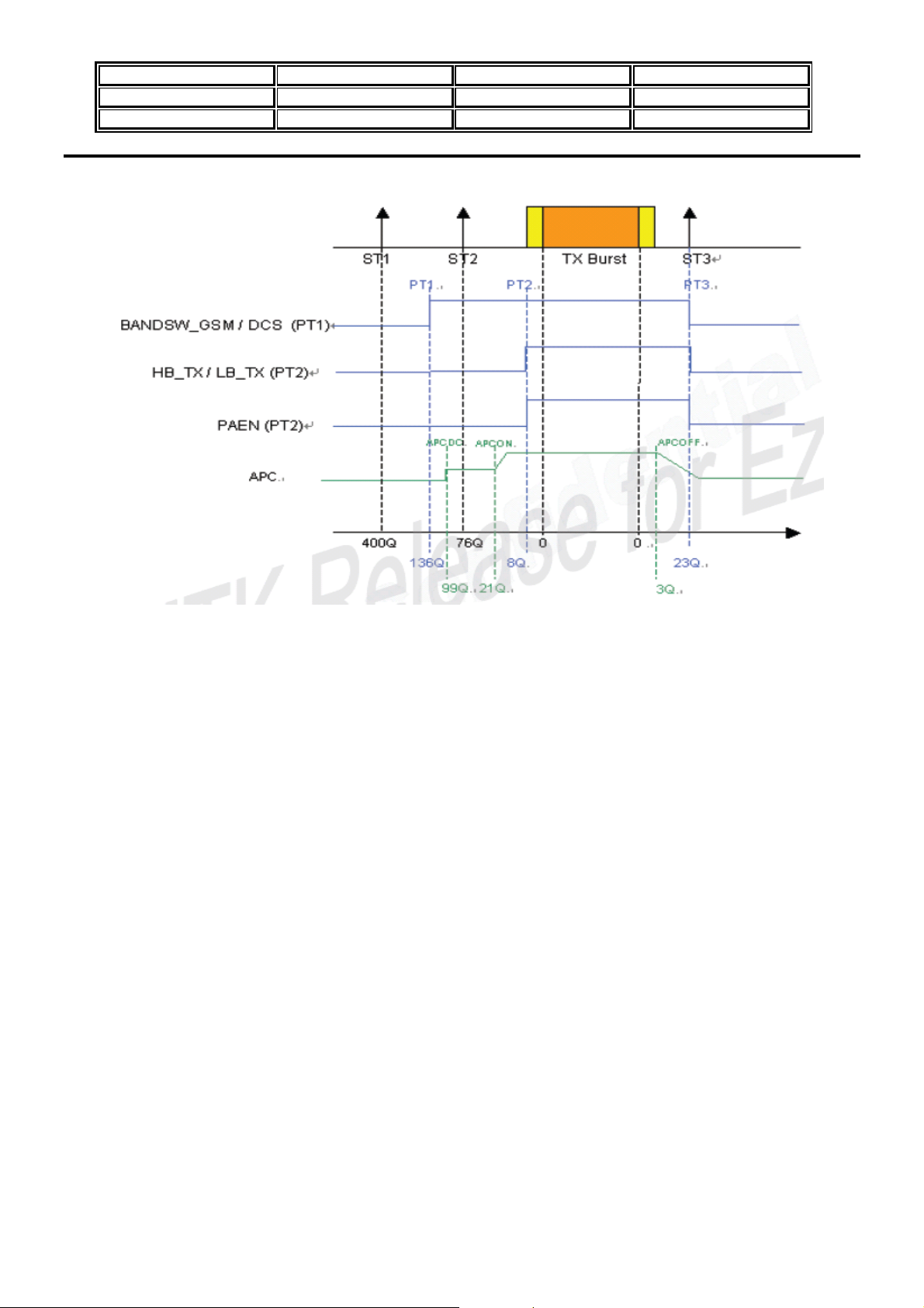
The Figure 36 shows the Timing Mask for Normal VAPC.
Figure 37. Timing Mask for normal VAPC.
Automatic Frequency Control Unit
Automatic Frequency Control unit provides the direct control of the oscillator for frequency offset and Doppler shift
compensation. It utilizes a 13-bit D/A converter to achieve high-resolution control. The AFC is always inputted to VCTCXO
to generate 26Mhz. The AFC Voltage must be calibrated to tune the VCTCXO to generate 26Mhz to be entered the MT6120
and MT6228 Main system clock. If the VCTCXO output a frequency with much ppm , The Frequency error and Phase error
are out of range. After calibrated, The Analog voltage is about 1.5V and AFC_DAC is about 4200 decimally.
Page 58

Model MASS 2 Version V_1.0
Prepared by H/W Date 22/01/2008
Subject Technical Manual Page 36/59
Figure 38. The AFC and VCTCXO Circiut diagram
8. Clocks and Reset
Clocks
There are two major time bases in the MT6228. For the faster one is the 13MHz clock origination from an off-chip
temperature-compensated voltage controlled oscillator that can be 26MHz. This signal is the input from the SYSCLK pad then
is converted to the square-wave signal. The other time base is the 32.768KHz clock generated by an on-chip oscillator
connected to an external crystal.
- 32.768Khz Time Base
The 32.768Khz clock is always running. It’s mainly used as the time base of the Real Time Clock(RTC) module,
which maintains time and date with counters. In low power mode, the 13Mhz time base is turned off, so the
32.768Khz clock shall be employed to update the critical TDMA timer and Watchdog timer. This Time base is also
used to clock the keypad Scanner logic. The C101,C102 must be tuned with Oscillator.
- 13Mhz Time Base
Two 1/2-dividers, one for MCU Clock and the other for DSP Clock, exist to allow usage of either 26 or 13Mhz
TXVCXO as clock input. There phase-locked loops(MPLL, DPLL and UPLL) are used to generate three primary
clocks.
MPLL : Provides the MCU System Clock.
DPLL : Provides the DSP System Clock. DPLL can be programmed to provide 1x to 6x
output of the 13Mhz reference.
UPLL : Provides the USB System Clock.
Reset Generation Unit
Page 59

Model MASS 2 Version V_1.0
Prepared by H/W Date 22/01/2008
Subject Technical Manual Page 37/59
Figure 38 shows reset scheme used in MT6225. There are three kinds of resets in the MT6225, i.e., hardware reset, watchdog
reset, and software resets.
Figure 39. Reset Scheme used in MT6225
- Hardware Reset
This Reset is inputted through the SYSRST# pin from PMIC(MT6318 Pin F9). The SYSRST# shall be driven to low
during power-on. The Hardware reset has a global effect on th e chip. It initializes all digital and analog circuits
except the RTC. Refer to the listed below.
- All Analog Circuits are turned off
- All PLLs are turned off and bypassed. The 13Mhz system clock is the default time base.
- Special Trap statue in GPIO.
- Watchdog Reset
A Watchdog reset is generated when the Watchdog timer expires as the MCU software failed to re-program the
timer counter in time. Hardware blocks that are affected by the watchdog reset are :
- MCU Subsystem
- DSP Subsystem
- External Component (By software program)
- Software Reset
These are local reset signals that initialize specific hardware. For example, The MCU or DSP software may write to
software reset trigger registers to reset hardware modules to their initial states, when hardware failures are detected.
The following Modules has software resets
- DSP Core
- DSP Coprocessors.
Page 60

Model MASS 2 Version V_1.0
Prepared by H/W Date 22/01/2008
Subject Technical Manual Page 38/59
II. MT6318 (GSM Power Management System)
The MT6318 is a power management system chip optimized for GSM/GPRS handsets, especially those based on the
MediaTek
MT621x/MT622x system solution. MT6318 contains 11 LDOs, one to power each of the critical GSM/GPRS sub-blocks
Sophisticated controls are available for power-up during battery charging, for the keypad interface, and for the RTC alarm.
The MT6318 is optimized for maximum battery life.
The 2-step RTC LDO design allows the RTC circuit to stay alive without a battery for several hours.
The MT6318 battery charger can be used with a lithium-ion (Li+) battery.
The SIM interface provides the level shift between SIM card and microprocessor.
The MT6318 is available in a 96-pin TFBGA package.
The operating temperature range is -25°C to +85°C.
The interface Features are listed below.
- Handles all GSM/GPRS Baseband Power Management
- Input range: 2.8 V ~ 5.0 V
- Charger input of up to 15 V
- 11 LDOs optimized for specific GSM/GPRS subsystems
- 2-step RTC LDO
- 600 mW Class AB audio amplifier
- Booster for series backlight LED driver
- Charge pump for parallel backlight LED driver
- SPI interface
- Pre-charge indication
- Li-ion battery charge function
- SIM card interface
- RGB LED driver
- Vcore for power-saver mode
- Over-current and thermal overload protection
- Programmable under voltage lockout protection
- Power-on reset and start-up timer
- 96-pin TFBGA package
Page 61

Model MASS 2 Version V_1.0
Prepared by H/W Date 22/01/2008
Subject Technical Manual Page 39/59
Figure 40. MT6318 Pin configuration.
Page 62

Model MASS 2 Version V_1.0
Prepared by H/W Date 22/01/2008
Subject Technical Manual Page 40/59
Page 63

Model MASS 2 Version V_1.0
Prepared by H/W Date 22/01/2008
Subject Technical Manual Page 41/59
Figure 41. Functional Block Diagram of MT6318
1. Charger Circuit
The charger circuit in PMIC is mainly comprised of 3 sub-functions.
Page 64

Model MASS 2 Version V_1.0
Prepared by H/W Date 22/01/2008
Subject Technical Manual Page 42/59
Figure 42. PMIC Charger Block Diagrams
Charger Detector
The charger detector senses the charging voltage from either a standard AC-DC adaptor or a USB connection.
When the charging input voltage is greater than the pre-determined threshold, the charging process is triggered.
The detector resists higher input voltages than other parts of the PMIC.
Charger Control
When the charger is on, this block controls the charging phase and turns on the appropriate LDOs according to the
battery status. The battery voltage is constantly monitored: if the voltage is greater than 4.3 V, charging is stopped
immediately to prevent permanent damage to the battery.
Control for Pre-Charge Indication
The PMIC provides 2 control signals SEL1 and SEL2 for the application that shows pre-charge status on the LCD.
In normal cases, VBAT is selected (SEL2 turned on) as the power input to the PMIC.
Page 65

Model MASS 2 Version V_1.0
Prepared by H/W Date 22/01/2008
Subject Technical Manual Page 43/59
Figure 43. Charger and Voltage Detection
Figure 44. Li-Ion Battery Charging Profile
2. Low Dropout Regulator (LDOs) and Reference
The MT6318 integrates eleven LDOs that are optimized for their given functions by balancing quiescent current,
dropout voltage, line/load regulation, ripple rejection, and output noise.
1) Digital Core LDO (VD)
The digital core LDO is a regulator that sources 200 mA (max) with a 1.8 V or 1.2 V output voltage selection
based on the supply voltage requirement of the BB chipset. The LDO also provides 1.5 V/0.9 V power-down
modes that can be controlled either by the SRCLKEN pin or by the PWR_SAVE_SPI software register. The digital
core LDO supplies the BB circuitry in the handset, and is optimized for a very low quiescent current.
2) Digital IO LDO (VIO)
Page 66

Model MASS 2 Version V_1.0
Prepared by H/W Date 22/01/2008
Subject Technical Manual Page 44/59
The digital IO LDO is a regulator that sources 100 mA (max) with a 2.8 V output voltage. The LDO supplies the
BB circuitry in the handset, and is optimized for a very low quiescent current. This LDO powers up at the same
time as the digital core LDO.
3) Analog LDO (VA)
The analog LDO is a regulator that sources 150 mA (max) with a 2.8 V output voltage. The LDO supplies the
analog sections of the BB chipsets and is optimized for low frequency ripple rejection in order to reject the ripple
coming from the RF power amplifier burst frequency at 217 Hz.
4) TCXO LDO (VTCXO)
The TCXO LDO is a regulator that sources 20 mA (max) with a 2.8 V output voltage. The LDO supplies the
temperature compensated crystal oscillator, which needs its own ultra low noise supply and very good ripple
rejection ratio.
5) RTC LDO (VRTC)
PMIC features a 2-step RTC that keeps RTC alive for a long time after the battery has been removed. The 1st LDO
charges a backup battery on the BAT_BACKUP pin to ~2.6 V. Also, when the battery is removed, the first stage
prevents the backup battery from leaking back to VBAT. The 2nd LDO regulates the 2.6 V supply to a 1.5 V/1.2 V
optional RTC voltage. The RTC voltage can be set by the RTC_SEL pin while the BB is alive.
6) Memory LDO (VM)
The memory LDO is a regulator that sources 150 mA (max) with a 1.8 V or 2.8 V output voltage selection based on
the supply specs of the memory chips. The LDO supplies the memory circuitry in the handset, and is optimized for
a very low quiescent current. This LDO powers up at the same time as the digital core LDO.
7) SIM LDO (VSIM)
The SIM LDO is a regulator that sources 20 mA (max) with a 1.8 V or 3.0 V output voltage selection based on the
supply specs of subscriber identity module (SIM) card. The LDO supplies the SIMs in the handset, and is
controlled independently of the other LDOs.
8) Memory Card LDO (VMC)
The memory card LDO is a regulator that sources 250 mA (max) with a 2.8 V or 3.0 V output voltage selection.
The LDO supplies the memory card (MS, SD, MMC) in the handset, and is controlled independently of the other
LDOs.
9) Auxiliary Analog Circuit LDO (VA_SW)
Page 67

Model MASS 2 Version V_1.0
Prepared by H/W Date 22/01/2008
Subject Technical Manual Page 45/59
The auxiliary analog circuit LDO is a regulator that sources 50 mA (max) with 2.8 V or 3.3 V output voltage
selection based on the VA_SW_SEL register setting (Register F [7]). It can be switched on/off by register control.
10) USB IO LDO (VUSB)
The USB IO LDO is a regulator that sources 20 mA (max) with a 3.3 V output voltage. The LDO output on/off
follows the control bit USB_PWR (Register 1 [3]). When the USB_PWR control bit is set to off, the VUSB output
voltage drops below 0.3 V within 1 ms. (VUSB output is shunt with a 1 μF capacitor.)
11) Vibrator LDO (VIBR)
The vibrator LDO is a regulator that sources 200 mA (max) with a 1.8 V or 3.2 V output voltage selection based on
the VIBSEL register setting (Register E [1]). This LDO can be powered on/off by register.
12) Reference Voltage Output (VREF)
The reference voltage output is a low noise, high PSRR and high precision reference with a guaranteed accuracy of
1.5% over temperature. The output is used as a system reference in MT6318 internally. However for accurate specs
of every LDO output voltage, avoid loading the reference voltage; only bypass it to GND with a minimum 100 Nf
capacitance.
Figure 45. Status of Mobile Handset and LDOs.
3. LED Drivers
PMIC provides 4 independent drivers. Three of them use an identical structure to drive 3 different LEDs (R, G, B).
The fourth is dedicated to driving the keypad LEDs. The reason for separating the LED drivers into 2 groups is
phone feature oriented.
Page 68

Model MASS 2 Version V_1.0
Prepared by H/W Date 22/01/2008
Subject Technical Manual Page 46/59
Figure 46. MT6318 Circuit of MASS 2
To Power on the handset, The Power_On_Off Signal must be Low. The external sense resistor R307 0.2ohm can determine
the charging current. The function equation is : Iconstant = 0.16/R307 = about 800mA. Ipre-charging = 10/R307 = about
50mA. The LDO Bypass capacitors are recommended to use Min X5R grade. Specially The DVDD, AVDD,VMEM and
VCORE must be used 4.7uF, 2012 type.
III. PF38F3040L0ZBQ1 (Smart combo RAM + Nor Flash Memory)
PF38F3040L0ZBQ1
The PF38F3040L0ZBQ1 is a mixed multi-chip package containing a 32Mbit smart combo RAM and a 128Mbit
Flash memory. The /BYTE inputs can be used to select the optimal memory configuration. The power supply for
the
PF38F3040L0ZBQ1 can range from 1.7V to 1.95V. The PF38F3040L0ZBQ1 can perform simultaneous read/write
operations on its flash memory and is available in a 88 pins BGA package making it suitable for a variety of
Page 69

Model MASS 2 Version V_1.0
Prepared by H/W Date 22/01/2008
Subject Technical Manual Page 47/59
applications. The Boot block architecture for flash memory is a bottom boot block. The MCP has one CE# signal
for Flash.
The PF38F3040L0ZBQ1 has two kinds power supplies.
One is VCCQ and S-VCC : 2.8V.
Other is F-VCC and F_VPP : 1.8V.
Figure 44. MCP Block diagram
Page 70

Model MASS 2 Version V_1.0
Prepared by H/W Date 22/01/2008
Subject Technical Manual Page 48/59
RF section
RF Section is combined with Transceiver MT6120, VCTCXO CSX-325T26, Power Amplifier Module RF3166
and Front-End Module LMSP54HA-348(or 349). The MEGA2 was designed for Tri-Band according to FEM,
PCB Modify and S/W Matching.
The one type is GSM900, DCS1800 and PCS1900 with LMSP54HA-348. Another type(named MEGA2Q) is
GSM850, DCS1800 and PCS1900 with LMSP54HA-349.
I. MT6120 (RF Transceiver IC)
MT6120 includes LNAs, two RF quadrature mixers, an integrated channel filter, programmable gain amplifiers(PGA), an IQ
demodulator for the receiver, a precision IQ modulator with offset PLL for the transmitter, two internal TX VCOs, a VCXO,
on-chip regulators, and a fully programmable sigma-delta fractional-N synthesizer with an on-chip RF VCO.
Features Receiver
- Very low IF architecture
- Quad band differential input LNAs
- Quadrature RF mixers
- Fully integrated channel filter
- More than 100 dB gain
- More than 110 dB control range
- Image-reject down conversion to baseband
Transmitter
- Precision IQ modulator
- Translation loop architecture
- Fully integrated wideband TX VCO
- Fully integrated TX loop filter
Frequency Synthesizer
- Single integrated, fully programmable fractional- N synthesizer
- Fully integrated wideband RF VCO
- Fast settling time suitable for multi-slot GPRS application
Voltage Control Crystal Oscillator (VCXO)
- 26 MHz crystal oscillator capable of supporting 13 MHz / 26 MHz output clock
- Programmable capacitor array for coarse tuning
- Internal varactor for fine tuning
Regulators
- Built-in low-noise, low-dropout (LDO) regulators
Low power consumption
QFN (Quad Flat Non-lead) Package 56-pin SMD
3-wire serial interface
Page 71

Model MASS 2 Version V_1.0
Prepared by H/W Date 22/01/2008
Subject Technical Manual Page 49/59
Figure 49. MT6120 Functional block diagram
- Recommended Operating Range
Item Symbol Min Typ Max Unit
Power Supply Voltage(VBAT) VBAT 3.1 3.6 4.6 V
Power Supply Voltage(VCCD) VCCD 2.5 2.8 3.1 V
Operating Ambient Temperature Topr -20 25 75 C
Page 72

Model MASS 2 Version V_1.0
Prepared by H/W Date 22/01/2008
Subject Technical Manual Page 50/59
A description of MT612X hardware control pins and their functionality are shown in the table below. MT612X has an
internal VCXO and its control.
Pin Description
Page 73

Model MASS 2 Version V_1.0
Prepared by H/W Date 22/01/2008
Subject Technical Manual Page 51/59
1. Receiver
The receiver section of MT6120 includes Quad-band low noise amplifiers(LNAs), RF quadrature mixers, an onchip channel filter, Programmable Gain Amplifiers(PGAs), quadrature second mixers, and a final low-pass filter.
The very low-IF MT6120 uses image-rejection mixers and filters to eliminate interference. With accurate RF
quadrature signal generation and mixer matching techniques, the image rejection of the MT6120 can reach 35dB
for all bands. Compared to a direct conversion receiver(DCR), MT6120’s very low-IF architecture improves the
blocking rejection, AM suppression, as well as the adjacent channel interference performance.
Page 74

Model MASS 2 Version V_1.0
Prepared by H/W Date 22/01/2008
Subject Technical Manual Page 52/59
- Receiver Input Frequency
Mode Min Max Unit
GSM850 869 894 MHz
GSM900 925 960 MHz
DCS 1805 1880 MHz
PCS1900 1930 1990 MHz
The below table is shown LNA input impedance. So, From FEM Sawfilter to MT6120 LNA input, The
Impedance matching is need for high sensitivity. The L903, L904, L905, C910, C911, C912, C913, C916 and
C917 are the matching State.
The IF signal is then filtered and amplified through an image-rejection filter and a PGA. The multi-stage PGA is implemented
between filtering stages to control the gain of the receiver. With 2 dB gain steps, a 78 dB dynamic range of the PGA ensures a
nd
proper signal level for demodulation. The quadrature 2
an analog differential IQ format.
mixers are provided on-chip to down convert IF signal to baseband in
2. Transmitter
The MT6120 transmitter section consists of two on-chip TX VCOs, buffer amplifiers, a down-converting mixer, a
quadrature modulator, an analog phase detector and a digital phase frequency detector, each with a charge pump
output and on chip loop filter. The dividers and loop filters are used to achieve the desired IF frequency from the
down-conversion mixer and quadrature modulator. For a given transmission channel, the transmitter will select one
of the two different TX reference dividing numbers. These built-in components, along with an internal voltage
controlled oscillator and a loop filter, implement a translation loop modulator. The TX VCO output is fed to the
power amplifier. A control loop, implemented externally, is used to control the PA’s output power level.
- Transceiver Output Frequency
Mode Min Max Unit
GSM850 824 849 MHz
GSM900 880 915 MHz
DCS1800 1710 1785 MHz
PCS1900 1850 1910 MHz
Page 75

Model MASS 2 Version V_1.0
Prepared by H/W Date 22/01/2008
Subject Technical Manual Page 53/59
3. TX VCO
Two power VCOs are integrated with OPLL to form a complete transmitter circuit. The TX VCO output power is
typically 9dBm with +/-2.5dB variation in GSM900 bands and +8dBm output power with +/-2dB variation in
DCS1800/PCS1900 bands over extreme Temperature conditions.
The PAM(RF3166) Input range is typically 3dBm. So 5dB Attenuator is added Between MT6120 and RF3166.
- For GSM850/GSM900 : R406, R407, R408,
- For DCS1800/PCS1900 : R403, R404, R405.
Tx VCO Frequency Range is same with Transmitter Frequency Range.
4. Frequency Synthesizer
The MT6120 includes a frequency synthesizer with a fully integrated RF VCO to generate RX and TX local
oscillator frequencies. The PLL locks the RF VCO to a precision reference frequency at 26MHz. To reduce the
acquisition time or to enable fast settling time for multi-slot data services such as GPRS, a digital loop along with a
fast-acquisition system are implemented in the synthesizer. After the calibration, a fast-acquisition system is
utilized for a period of time to facilitate fast locking.
The frequency ranges of the synthesizer for RX mode are
RX mode GSM850 1737MHz ~ 1788MHz
GSM900 1850MHz ~ 1920MHz
DCS1800 1805MHz ~ 1880MHz
PCS1900 1930MHz ~ 1990MHz
The Calculate LO Frequency Fvco from RX Channel Frequency Fch is following.
Fvco = 2*Fch-200K for GSM850 and GSM900
Fvco = Fch-100K for DCS1800 and PCS1900.
The frequency ranges of the synthesizer for TX mode are
TX mode GSM850 1813MHz ~ 1868MHz
GSM900 1936Mhz ~ 2059Mhz
DCS1800 1881Mhz ~ 2008Mhz
PCS1900 2035MHz ~ 2149MHz
The Calculate LO Frequency Fvco from TX Channel Frequency Fch is following.
(Set the divider ratio D1 of TX reference divider = 11)
Fvco = 2*D1*Fch/(D1-1) for GSM850 and GSM900
Fvco = D1*Fch/(D1-1) for DCS1800 and PCS1900.
Page 76

Model MASS 2 Version V_1.0
Prepared by H/W Date 22/01/2008
Subject Technical Manual Page 54/59
The MT6120 uses a digital calibration technique to reduce the PLL settling time once the RF synthesizer is
programmed through a 3-wire serial interface, the calibration loop is activated. The main function of the calibration
loop is to preset the RF VCO to the vicinity of the desired frequency quickly and correctly, thus aiding the PLL to
settle faster. On the other hand, since a large portion of initial frequency error is dealt with by the integrated
calibration loop, the overall locking time can be drastically reduced, irrespective of the desired frequency.
5. Voltage Control Crystal Oscillator(VCXO)
VCXO consists of an amplifier, a buffer, and a programmable capacitor array. The VCXO provides the MT6120
with a selectable reference frequency of either 13MHz or 26MHz. When VCXOFRQ pin is high, Output Frequency
is 26Mhz. When VCXOFRQ pin is low, Output Frequency is 13Mhz.
VCXOFRQ is high in MEGA2. The Amplifier is designed to be in series resonance with a standard 26Mhz crystal.
The Crystal is connected from the Input pin XAL of Amplifier to ground through a series load capacitance. The
buffer provides a typical 600mVpp voltage swing. As an alternative, the reference frequency can be provided by
an external 26Mhz VCTCXO module. When Pin VCXOCXR is tied to the VCCVCXO supply, the XTAL pin will
accept an external signal. Furthermore, the VCXO control pin can be tied to VCCVCXO to prevent the current
leakage during the sleep mode operation.
6. Regulator
The MT6120 internal regulators provide low noise, stable, temperature and process independent supply voltages to
critical blocks in the transceiver. An internal P-channel MOSFET pass transistor is used to achieve a low dropout
voltage of less than 150mV in all regulators.
II. RF3166
Page 77

Model MASS 2 Version V_1.0
Prepared by H/W Date 22/01/2008
Subject Technical Manual Page 55/59
( GSM850,GSM900 and DCS,PCS Power Amplifier Module)
Figure 50. RF3166 Block Diagram
The RF3166 is a high-power, high-efficiency power amplifier module with integrated power control that provides
over 50dB of control range. The device is a self-contained6mmx6mm module with 50Ω input and output terminals.
The device is designed for use as the final RF amplifier inGSM850, EGSM900, DCS and PCS handheld digital
cellular equipment and other applications in the 824MHz to849MHz, 880MHz to 915MHz, 1710MHz to
1785MHzand 1850MHz to 1910MHz bands. The RF3166 incorporates RFMD’s latest VBATT tracking circuit,
which monitors battery voltage and prevents the power control loop from reaching saturation. The VBATT tracking
circuit eliminates the need to monitor battery voltage, thereby minimizing switching transients. The RF3166
requires no external routing or external components, simplifying layout and reducing board space.
The VRamp Range is from 0.26V to 2.1V. And the R400, R401, C406 is a Voltage divider for fine tuning and
Low pass filter of 300Khz.
The Input/Output Impedance is 50ohm. So, The PCB Design must be designed with 50ohm strobe line.
Thermal vias are required in the PCB layout to effectively conduct heat away from the package. The via pattern
has been designed to address thermal, power dissipation and electrical requirements of the device as well as
accommodating routing strategies. The via pattern used for the RFMD qualification is based on thru-hole vias with
0.203mm to 0.330mm finished hole size on a 0.5mm to 1.2mm grid pattern with 0.025mm plating on via walls. If
micro vias are used in a design, it is suggested that the quantity of vias be increased by a 4:1 ratio to achieve similar
results.
Page 78

Model MASS 2 Version V_1.0
Prepared by H/W Date 22/01/2008
Subject Technical Manual Page 56/59
Figure 51. RF3166 Power control sequence
Page 79
Model MASS 2 Version V_1.0
Prepared by H/W Date 22/01/2008
Subject Technical Manual Page 57/59
The Next Picture is for RF TX Timing of BSI and BPI.
< Single Slot TX Event with Timing Requirement>
<BSI Interface>
In order to simply the serial control mechanism, and achieve best usage of BSI resources. Each burst transmitted,
There are three generic timing defined (ST1/ST2/ST3) to send 3-wire control commands to transceiver. Usually
1’st BSI event(ST1) is used to warm up the synthesizer and set its N-counter to lock the operational frequency. The
2’nd BSI(ST2) is used to set the transmitted mode and indicate the operational band. The 3’rd BSI(ST3)is used to
command transceiver entering idle mode. All bands(GSM/DCS/PCS) share the same timing.
<BPI interface>
In order to simply the parallel control mechanism, and achieve best usage of BPI resources. Each burst transmitted,
there are also three generic timing defined(PT1/PT2/PT3) to send HW control Signals to RF module. In other
words, there are only three timing events to trigger HW control signals changing their states. Usually 1’st BPI
event(PT1) is used to select suitable band for TXVCO. The 2’nd BPI(PT2) is used to turn on PA and control
antenna switch depends on its band. The 3’rd BSI(ST3) is used to force RF module to terminate transmission and
enter idle mode. All bands share the same timing but could has different HW control signals.
The Next Picture is for RF Receiving Timing of BSI and BPI.
Page 80

Model MASS 2 Version V_1.0
Prepared by H/W Date 22/01/2008
Subject Technical Manual Page 58/59
<BSI Interface>
<Single Slot RX Event with Timing Requirement>
In order to simply the serial control mechanism, and achieve best usage of BSI resources. Each burst received, there
are three generic timing defined (SR1/SR2/SR3) to send 3-wire control commands to transceiver. Usually 1’st BSI
event(SR1) is used to warm up the synthesizer and set its N-Counter to lock the operation frequency. The 2’nd
BSI(SR2) is used to set the receiving amplifier gain, received mode and operation band of transceiver. The 3’rd
BSI(SR3) is used to command transceiver entering idle mode. All bands(GSM/DCS/PCS) share the same timing.
<BPI Interface>
In order to simply the parallel control mechanism, and achieve best usage of BPI resources. Each burst received,
there are also three generic timing defined(PR1/PR2/PR3) to send HW Control signals to RF Module. In other
words, There are only three timing events to trigger HW control signals changing its state. Usually 1’st BPS
event(PR1) is used to activate the RF Component. The 2’nd BPI(PR2) is used to control antenna switch depend on
its band. The 2’rd BPI(PR3) is used to force RF Module entering idle mode. All bands(GSM/DCS/PCS) share the
same timing but could have different HW control signals.
III. LMSP54HA-348TEMP
(Antenna Switch Module for Tri- Band with SAW Filter)
LMSP54HA-348TEMP is an Antenna Switch Module for GSM850/DCS1800/PCS1900 of Murata with Three
SAW Modules.
Control Pins (VC1, VC2, VC3) are connected to LB_TX, HB_TX,PCB (signals from baseband processor). The
Control Pins Operating range is 2.4V 2.8V.
Page 81

Model MASS 2 Version V_1.0
Prepared by H/W Date 22/01/2008
Subject Technical Manual Page 59/59
Figure 35. The Evaluation board and control logic of LMSP54HA-349TEMP
The GSM900/DCS1800/PCS1900 input port matching impedances are 50 ohm.
The GSM900/DCS1800/PCS1900(Balance) output port matching impedance are 150ohm.
Page 82

Model MASS 2 Version V_1.0
Prepared by H/W Date 22/01/2008
Subject Technical Manual Page 1/42
IC Information
Pin out for U900 (LMSP54HA-348)
Page 83

Model MASS 2 Version V_1.0
Prepared by H/W Date 22/01/2008
Subject Technical Manual Page 2/42
Pin out for U901 (CSX-325T26BADT-J2E)
PIN NO FUNCTION NAME
1
2
3
4
5, 6, 7, 8
V control
Ground
OSC Output
Power
No connect
Vcont
GND
OUTPUT
Vcc
N.C
Page 84

Model MASS 2 Version V_1.0
Prepared by H/W Date 22/01/2008
Subject Technical Manual Page 3/42
Pin out for BAT300 (SF-3R3-S104Z)
① ②
PIN NO FUNCTION NAME
1
2
VCC
Ground
VCC
GND
Page 85

Model MASS 2 Version V_1.0
Prepared by H/W Date 22/01/2008
Subject Technical Manual Page 4/42
Pin out for CON300 (BT03-F200B-03)
PIN NO FUNCTION NAME
1
2
3
VBAT
BATTERY ID
GROUND
VBAT
BAT ID
GND
Page 86
Model MASS 2 Version V_1.0
Prepared by H/W Date 22/01/2008
Subject Technical Manual Page 5/42
Pin out for CON130 (AXK7L54145J)
Page 87

Model MASS 2 Version V_1.0
Prepared by H/W Date 22/01/2008
Subject Technical Manual Page 6/42
Pin out for U2 (PF38F3040L0ZBQ1)
Page 88

Model MASS 2 Version V_1.0
Prepared by H/W Date 22/01/2008
Subject Technical Manual Page 7/42
Page 89

Model MASS 2 Version V_1.0
Prepared by H/W Date 22/01/2008
Subject Technical Manual Page 8/42
Page 90

Model MASS 2 Version V_1.0
Prepared by H/W Date 22/01/2008
Subject Technical Manual Page 9/42
Pin out for U820 (XC6401FF49)
Page 91

Model MASS 2 Version V_1.0
Prepared by H/W Date 22/01/2008
Subject Technical Manual Page 10/42
PIN NO FUNCTION NAME
1
2
3
4
5
6
ON/OFF Control 1
Power Input
ON/OFF Control 2
Output 2
Ground
Output 1
VOUT2
VOUT1
EN1
VIN
EN2
VSS
Page 92

Model MASS 2 Version V_1.0
Prepared by H/W Date 22/01/2008
Subject Technical Manual Page 11/42
Pin out for U910 (RF3166)
Page 93

Model MASS 2 Version V_1.0
Prepared by H/W Date 22/01/2008
Subject Technical Manual Page 12/42
Pin out for LED701~LED706 (SSC-SB104-IT BIN18)
Pin out for OSC100 (ST-4115 32.768KHZ)
Page 94

Model MASS 2 Version V_1.0
Prepared by H/W Date 22/01/2008
Subject Technical Manual Page 13/42
Pin out for U300 (MT6318)
Page 95

Model MASS 2 Version V_1.0
Prepared by H/W Date 22/01/2008
Subject Technical Manual Page 14/42
Page 96

Model MASS 2 Version V_1.0
Prepared by H/W Date 22/01/2008
Subject Technical Manual Page 15/42
PIN NAME FUNCTION
K7
A9
G9
H9
B10
B4
K4
H3
C9
E9
E1
D1
C1
B9
D2
E2
F2
H2
G2
J7
H10
K9
H8
J9
K10
B7
F9
F1
J1, J2, J3,
D9, D10,
A8,
B8, C8, A5,
B5, C5, D5
J4
H5
K2
D3, E3, E4,
F3, F4, G3,
G4, G5, G6,
G7, H4, H6,
H7, D7, D8,
E7, E8, F7,
C3, C4, C6,
C7, D4, D6
J10
C10
K1
PWRKEY
PWRBB
SRCLKEN
SIMVCC
BAT_ON
DC_OV
VM_SEL
SEL1_EN
RTC_SEL
VD_SEL
AC
USB
V_USB
INT
GDRVUSB
GDRVAC
ISENSE
SEL1
SEL2
SIMIO
SIMRST
SIMCLK
SIO
SRST
SCLK
RSTCAP
RESET
VBAT
PWRIN
VB_OUT
ISENSE_OUT
BP/VREF
GND
VD
VIO
VA
Power on button input. Active low
Power on/off from microprocessor. Active high
VTCXO and VA enable. High = enable. Low = disable
VSIM enable. High = enable. Low = disable.
Indication that Li-ion battery is inserted
DC/DC protection input. OV threshold voltage is 1V.
External memory supply selection. 1 = 2.8V, 0 = 1.8V
Enable the “pre-charge indication” function. 1 = enable, 0 = disable.
VRTC output voltage selection. 1 = 1.5V, 0 = 1.2V
VD output voltage selection. 1 = 1.8V/1.5V, 0 = 1.2V/0.9V
AC-DC adaptor input
USB power input
3.3V USB power output
Interrupt PIN. Active low
Control output to the gate of the external p-channel FET for the USB charger.
Control output to the gate of the external p-channel FET for the AC charger.
Charger current sensing input
Control output to the gate of the external PMOS for the AC charger input
Control output to the gate of the external PMOS for the VBAT input
Non level-shifted SIM data (3V)
Non level-shifted SIM reset input (3V)
Non level-shifted SIM clock input (3V)
Level-shifted SIM data (1.8/3V)
Level-shifted SIM reset output (1.8/3V)
Level-shifted SIM clock output (1.8/3V)
Reset delay time capacitance
System reset. Low active.
Battery input voltage
Power input
Battery output voltage. Switchable.
ISENSE output voltage. Switchable.
Bandgap reference and bypass capacitance
Ground
Digital core supply
Digital IO supply
Analog supply
Auxiliary analog supply. Switchable.
Page 97

E10
H1
G1
K8
G10
K3
F10
A3
A4
A2
A10
J5
J6
K5
K6
B2
B1
C2
A1
B3
A7
B6
A6
F8
G8
J8
Prepared by H/W Date 22/01/2008
BAT_BACKUP
Model MASS 2 Version V_1.0
Subject Technical Manual Page 16/42
VA_SW
VTCXO
VM
VSIM
VRTC
VMC
VIBR
C1+
C1-
C2+
AUDP
AUDN
SPK+
SPKVO_R
VO_G
VO_B
LED_KP
CS_KP
BLDRV
CS_BL
FB_BL
SPICS
SPICK
SPIDAT
TCXO supply
Memory supply
SIM supply
RTC supply
Memory card supply
Vibrator driver
Charge pump capacitor. Positive terminal.
Charge pump capacitor. Negative terminal.
DC/DC output back-up capacitor. Positive terminal.
Backup battery pin for 2-step RTC
Audio positive input
Audio negative input
Speaker positive output
Speaker negative output
R LED current driver
G LED current driver
B LED current driver
KP LED driver
KP LED current sensor
Control output to the gate of the external.
Voltage sensor input for external BL FET current
Voltage sensor input from white LED ballast resistor
Serial port select input
Serial port clock input
Serial port I/O
Page 98

Model MASS 2 Version V_1.0
Prepared by H/W Date 22/01/2008
Subject Technical Manual Page 17/42
Pin out for D100, D300, D800 (RB520S-30)
PIN NO FUNCTION NAME
1
2
Anode
Cathode
A
C
Page 99

Model MASS 2 Version V_1.0
Prepared by H/W Date 22/01/2008
Subject Technical Manual Page 18/42
Pin out for U302 (SI7911DN)
PIN NO FUNCTION NAME
1
2
3
4
5
6
7
8
Source 1
Gate 1
Source 2
Gate 2
Drain 2
Drain 2
Drain 1
Drain 1
S1
G1
S2
G2
D2
D2
D1
D1
Page 100

Model MASS 2 Version V_1.0
Prepared by H/W Date 22/01/2008
Subject Technical Manual Page 19/42
Pin out for U301 (AO8701)
Pin out for ZD101, ZD102 (EMIF04-1502M8)
 Loading...