

Page 1

MODEL MEGA3 VERSION V_1.01
PREPARED BY H/W DATE 2008.APR.23
SUBJECT TECHNICAL MANUAL PAGE 1/77
Change History
Rev Issued Date History Name
1.00 2008.Jan.08 First Version H.S.Lee
1.01 2008.Apr.23 1. /LRD Line added for LCM from Main Board B Version H.S.Lee
Æ To read the LDI ID for AS Center. (page 33)
MEGA3 TECHNICAL MANUAL Page 3.1
Page 2

MODEL MEGA3 VERSION V_1.01
PREPARED BY H/W DATE 2008.APR.23
SUBJECT TECHNICAL MANUAL PAGE 2/77
Block Diagram
MEGA3 TECHNICAL MANUAL Page 3.2
Page 3

MODEL MEGA3 VERSION V_1.01
PREPARED BY H/W DATE 2008.APR.23
SUBJECT TECHNICAL MANUAL PAGE 3/77
Baseband section
This document provides a description of the baseband section of the MEGA3. Most design decisions are explained,
but no detailed calculations are included. Total chip solutions(MT6228, MT6318, MT6120) except for RF Power
Amplifier(RF3166) are from Media Tek, Taiwan.
I. MT6228 ( GSM/GPRS Baseband Processor )
1. System OverView
The Revolutionary MT6228 is a leading edge single-Chip solution for GSM/GPRS mobile phones targeting the emerging
applications in digital audio and video. Based on 32bit ARM7EJ-S
performance GPRS Class 12 MODEM, but also provides comprehensive and advanced solutions for handheld multimedia. But, the MEGA3 can only support GPRS Class 8.
The Figure 1 is shown Typical Application for MT6228.
TM
RISC processor, MT6228 not only features high
Figure 1 : Typical Application for MT6228
1.1 Platform Feature
MEGA3 TECHNICAL MANUAL Page 3.3
Page 4

MODEL MEGA3 VERSION V_1.01
PREPARED BY H/W DATE 2008.APR.23
SUBJECT TECHNICAL MANUAL PAGE 4/77
z General
-. Integrated voie-band, audio-band and base-band analog front ends.
-. TFBGA 13mm x 13mm, 314balls, 0.65mm pitch package.
z MCU Subsystem
-. ARM7EJ-S 32bit RISC processor
-. High Performance Multi-layer AMBA bus
-. Java hardware acceleration for fast Java-based games and applets.
-.Operating frequency : 25/52/104Mhz
-. Dedicated DMA Bus
-. 14 DMA channels
-. 1M bits on-chip SRAM
-. 1M bits MCU dedicated Tightly Coupled memory
-. 256K bits CODE cache
-. 64K bits DATA cache
-. On-chip boot ROM for factory flash programming
-. Watchdog timer for system crash recovery
-. 3sets of General purpose timer
-. Circuit Switch Data coprocessor
-. Division coprocessor
-. PPP Framer coprocessor
z External Memory Interface
-. Supports up to 4 external devices
-. Supports 8-bit or 16-bit memory components with maximum size of up to 64M bytes each.
-. Supports Mobile RAM and Cellular RAM
-. Supports Flash and SRAM/PSRAM with page mode or burst mode
-. Industry standard Parallel LCD interface
-. Supports Multi-media companion chips with 8/16bits data width.
-. Flexible I/O voltage of 1.8V ~ 2.8V for memory interface.
z User Interface
-. 6-row x 7-column keypad controller with hardware scanner.
-. Supports multiple key presses for gaming.
-. SIM/USIM controller with hardware T=0/T=1 protocol control.
-. Real Time Clock(RTC) operating with a separate power supply.
-. General Purpose I/Os (GPIOs)
-. 2sets of Pulse Width Modulation(PWM) output.
-. Alerter Output with enhanced PWM or PDM.
-. 8 external interrupt lines.
z Security
-. Cipher : supports AES, DES/3DES
MEGA3 TECHNICAL MANUAL Page 3.4
Page 5

MODEL MEGA3 VERSION V_1.01
PREPARED BY H/W DATE 2008.APR.23
SUBJECT TECHNICAL MANUAL PAGE 5/77
-. Hash : Supports MD5, SHA-1
-. Supports security key and 2kit chip unique ID
z Connectivity
-. 3 UARTs with hardware flow control and speed up to 921600pbs.
-. IrDA modulator/Demodulator with hardware framer. Supports SIR/MIR/FIR operating Speeds.
-. Full speed USB 1.1 OTG capability. Support Device mode, limited host mode and dual-role OTG mode.
-. Multi Media Card, Secure Digital Memory Card, Memory Stick, Memory Stick Pro Host Controller with flexible
I/O Voltage power.
-. Supports SDIO interface for SDIO peripherals as well as WIFI connectivity.
-. DAI/PCM and I2S interface for Audio application.
z Power Management
-. Power Down Mode for analog and digital circuits.
-. Processor Sleep Mode
-. Pause Mode of 32Khz clocking in Standby state
-. 7 channel Auxiliary 10bit A/D converter for charger and battery monitoring and photo sensing.
z Test and Debug
-. Built-in digital and analog loop back modes for both Audio and baseband front-end.
-. DAI port complying with GSM Rec.11.10
-. JTAG port for debugging embedded MCU.
1.2 Model Feature
z Radio Interface and Baseband Front End
-. GMSK Modulator with analog I and Q channel outputs.
-. 10-bit D/A converts for Uplink baseband I and Q signals.
-. 14bit high resolution A/D converter for downlink baseband I and Q signals.
-. Calibration mechanism of offset and gain mismatch for baseband A/D converter and D/A converter.
-. 10bit D/A converter for Automatic Power Control(APC)
-. 13bit high resolution D/A converter for Automatic frequency Control(AFC)
-. Programmable Radio RX filter.
-. 2 channels Baseband Serial Interface(BSI) with 3-wire control.
-. Bi-Directional BSI interface. RF chip register read access with 3-wire or 4-wire interface
-. 10 pin Baseband Parallel Interface(BPI) with programmable driving strength.
-.Multi-band Support (GSM850, GSM900, DCS1800, PCS1900)
z Voice and Model Codec
-. Dial tone Generation.
-. Voice memo
-. Noise reduction
-. Echo suppression
-. Advanced side tone Oscillation Reduction.
-. Digital side tone generator with programmable gain.
MEGA3 TECHNICAL MANUAL Page 3.5
Page 6

MODEL MEGA3 VERSION V_1.01
PREPARED BY H/W DATE 2008.APR.23
SUBJECT TECHNICAL MANUAL PAGE 6/77
-.Two programmable acoustic compensation filters.
-. GSM/GPRS quad vocoders for adaptive multirate(AMR), enhanced full rate(EFR), full rate(FR) and half rate(HR).
-. GSM channel coding, equalization and A5/1 and A5/2 ciphering.
-.GPRS GEA1 and GEA2 ciphering.
-. Programmable GSM/GPRS model.
-. Packet Switched data with CS1/CS2/CS3/CS4 coding schemes.
-.GSM circuit switch data.
-. GPRS Class 12.
z Voice Interface and Voice Front End.
-. Two MICrophone inputs sharing one low noise amplifier with programmable gain and automatic gain control(AGC)
mechanisms.
-. Voice power amplifier with programmable gain.
-. 2’nd order Sigma-Delta A/D converter for voice uplink path.
-. D/A Converter for Voice downlink path.
-. Supports Half-duplex hands-free operation.
-. Compliant with GSM 03.50.
1.3 Multimedia Feature
z LCD/NAND Flash Interface
-. Dedicated Parallel Interface supports 3 external devices with 8/16 bis NAND flash interface, 8/9/16/18 bit Parallel
interface and serial interface for LCM.
-. Built-in NAND flash controller with 1 bit ECC for mass storage.
z LCD Controller
-. Supports simultaneous connection to up to 3 parallel LCD and 2 serial LCD modules.
-. Supports LCM format : RGB332, RGB444, RGB565, RGB666, RGB888.
-. Supports LCD Module with maximum resolution up to 800x600 at 24bpp.
-. Per pixel alpha channel.
-. True color engine
-. Supports hardware display rotation.
-. Capable of combining display memories with up to 6 blending layers.
z Image Signal Processor
-. 8/10 bit Bayer format image input.
-. YUV422 format image input.
-. Capable of processing image of size up to 3M pixels.
-. Color correction matrix.
-. Gamma correction.
-. Automatic exposure(AE) control.
-. Automatic focus control.
-. Automatic white balance(AWB) control.
-. Programmable AE/AEB windows.
MEGA3 TECHNICAL MANUAL Page 3.6
Page 7

MODEL MEGA3 VERSION V_1.01
PREPARED BY H/W DATE 2008.APR.23
SUBJECT TECHNICAL MANUAL PAGE 7/77
-. Edge enhancement support.
-. Shading compensation.
-. Defect Pixel compensation.
z Graphic Compression.
-. GIF decoder, PNG Decoder.
z JPEG Decoder
-. ISO/IEC 10918-1 JPEG Baseline and Progressive modes.
-. Supports all possible YUV formats, Including grayscale format.
-. Supports all DC/AC Huffman table parsing.
-. Supports all quantization table parsing.
-. Supports a restart interval
-. Supports SOS, DHT, DQT and DRI marker parsing.
-. IEEE Std 1180-1990 IDCT standards compliance
-. Supports progressive image processing to minimize storage space requirement.
-. Supports reload-able DMA for VLD stream.
z JPEG Encoder
-. ISO/IEC 10918-1 JPEG baseline mode.
-.ISO/IEC 10918-2 compliance
-. Supports YUV422 and YUV420 and grayscale formats.
-. Supports JFIF.
-. Standard DC and AC Huffman tables.
-. Provides 4 levels of encode quality.
-. Supports continuous shooting.
z Image Data Processing.
-. Supports Digital Zoom.
-. Supports RGB888/565, YUV444 image processing.
-. High throughput hardware scale. Capable of tailoring an image to an arbitrary size.
-. Horizontal scaling in averaging method.
-. Vertical scaling in bilinear method.
-. Simultaneous scaling for MPEG-4 encode and LCD display.
-. YUV and RGB color space conversion.
-. Pixel format transform.
-. Boundary padding.
-. Pixel processing : hue/saturation/intensity/color adjustment, Gamma correction and grayscale/invert/sepia-tone effects.
-. Programmable spatial filtering : linear filter, non-linear filter and multi-pass artistic effects.
-. Hardware accelerated image editing.
-. Photo frame capability.
-. RGB thumbnail data output.
z MPEG-4/H.263 CODEC
MEGA3 TECHNICAL MANUAL Page 3.7
Page 8

MODEL MEGA3 VERSION V_1.01
PREPARED BY H/W DATE 2008.APR.23
SUBJECT TECHNICAL MANUAL PAGE 8/77
-. Hardware Video CODEC.
-. ISO/IEC 14496-2 simple profile :
Decode @ level 0/1/2/3
Encode @ level 0.
-. ITU-T H.263 profile 0 @level 10.
-. Max decode speed is VGA @15fps.
-. Max encode speed is CIF@15fps.
-. Support VGA mode encoding.
-. Horizontal and vertical de-blocking filter in video playback.
-. Encoder resync marker and HEC.
-. Supports visual tools for decoder : I-VOP, P-VOP, AC/DC Prediction, 4-MV, Unrestricted MV, Error Resilience,
Short Header.
-. Error Resilience for decoder : Slice Resynchronization, Data Partitioning, Reversible VLC.
-. Supported visual tools for encoder : I-VOP, P-VOP, Half-Pel, DC Prediction, Unrestricted MV, Reversible VLC, Short
Header.
-. Supports encoding motion vector of range up to -64/+63.5 pixels.
-. HE-AAC decode support.
-. AAC/AMR/WB-AMR audio decode support
-. AMR/WB-AMR audio encode support.
z TV-OUT
-. Supports NTSC/PAL formats(interlaced mode)
-. 10bit video DAC with 2x over-sampling.
-. Supports one composite video output.
z Audio CODEC
-. Supports HE-AAC codec decode
-. Supports AAC codec decode
-. Wavetable synthesis with up to 64 tones
-. Advanced wavetable synthesizer capable of generating simulated stereo
-. Wavetable including GM full set of 128 instruments and 47 sets of percussions
-. PCM Playback and Record
-. Digital Audio Playback
z Audio Interface and Audio Front End
-. Supports I2S interface
-. High resolution D/A Converters for Stereo Audio playback
-. Stereo analog input for stereo audio source
-. Analog multiplexer for stereo audio
-. Stereo to mono conversion
MEGA3 TECHNICAL MANUAL Page 3.8
Page 9

MODEL MEGA3 VERSION V_1.01
PREPARED BY H/W DATE 2008.APR.23
SUBJECT TECHNICAL MANUAL PAGE 9/77
Figure 2 is shown the Block Diagram of MT6228 for detail.
Figure 2 : Block Diagram of MT6228
2. Product Description
MEGA3 TECHNICAL MANUAL Page 3.9
Page 10

MODEL MEGA3 VERSION V_1.01
PREPARED BY H/W DATE 2008.APR.23
SUBJECT TECHNICAL MANUAL PAGE 10/77
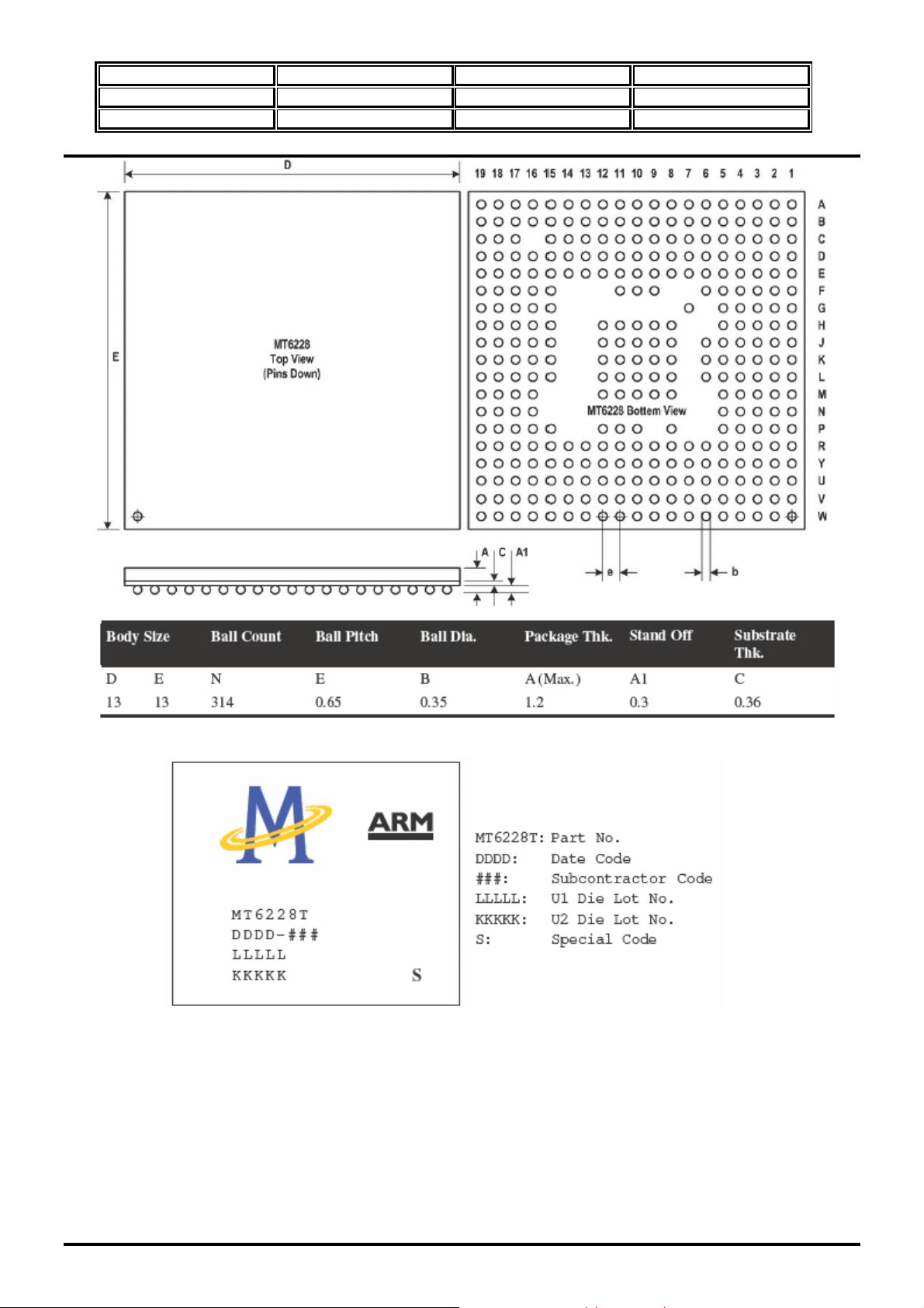
2.1 Pin Outs
One type of Package for this product, TFBGA 13x13mm, 296balls, 0.65mm pitch package, is offered.
Pin outs and the top view are illustrated in Figure 3,4.
-. Pin Out
Figure 3 . MT6228 Pin Out.
-. Top and Bottom View
MEGA3 TECHNICAL MANUAL Page 3.10
Page 11
MODEL MEGA3 VERSION V_1.01
PREPARED BY H/W DATE 2008.APR.23
SUBJECT TECHNICAL MANUAL PAGE 11/77
2.2 Top Masking Definition
Figure 5. Top masking definition
MEGA3 TECHNICAL MANUAL Page 3.11
Page 12

PREPARED BY H/W DATE 2008.APR.23
2.3 Pin Description
MODEL MEGA3 VERSION V_1.01
SUBJECT TECHNICAL MANUAL PAGE 12/77
MEGA3 TECHNICAL MANUAL Page 3.12
Page 13

MODEL MEGA3 VERSION V_1.01
PREPARED BY H/W DATE 2008.APR.23
SUBJECT TECHNICAL MANUAL PAGE 13/77
MEGA3 TECHNICAL MANUAL Page 3.13
Page 14

MODEL MEGA3 VERSION V_1.01
PREPARED BY H/W DATE 2008.APR.23
SUBJECT TECHNICAL MANUAL PAGE 14/77
MEGA3 TECHNICAL MANUAL Page 3.14
Page 15

MODEL MEGA3 VERSION V_1.01
PREPARED BY H/W DATE 2008.APR.23
SUBJECT TECHNICAL MANUAL PAGE 15/77
MEGA3 TECHNICAL MANUAL Page 3.15
Page 16

MODEL MEGA3 VERSION V_1.01
PREPARED BY H/W DATE 2008.APR.23
SUBJECT TECHNICAL MANUAL PAGE 16/77
MEGA3 TECHNICAL MANUAL Page 3.16
Page 17

MODEL MEGA3 VERSION V_1.01
PREPARED BY H/W DATE 2008.APR.23
SUBJECT TECHNICAL MANUAL PAGE 17/77
MEGA3 TECHNICAL MANUAL Page 3.17
Page 18

MODEL MEGA3 VERSION V_1.01
PREPARED BY H/W DATE 2008.APR.23
SUBJECT TECHNICAL MANUAL PAGE 18/77
MEGA3 TECHNICAL MANUAL Page 3.18
Page 19

MODEL MEGA3 VERSION V_1.01
PREPARED BY H/W DATE 2008.APR.23
SUBJECT TECHNICAL MANUAL PAGE 19/77
MEGA3 TECHNICAL MANUAL Page 3.19
Page 20

MODEL MEGA3 VERSION V_1.01
PREPARED BY H/W DATE 2008.APR.23
SUBJECT TECHNICAL MANUAL PAGE 20/77
MEGA3 TECHNICAL MANUAL Page 3.20
Page 21

MODEL MEGA3 VERSION V_1.01
PREPARED BY H/W DATE 2008.APR.23
SUBJECT TECHNICAL MANUAL PAGE 21/77
MEGA3 TECHNICAL MANUAL Page 3.21
Page 22

MODEL MEGA3 VERSION V_1.01
PREPARED BY H/W DATE 2008.APR.23
SUBJECT TECHNICAL MANUAL PAGE 22/77
MEGA3 TECHNICAL MANUAL Page 3.22
Page 23

MODEL MEGA3 VERSION V_1.01
PREPARED BY H/W DATE 2008.APR.23
SUBJECT TECHNICAL MANUAL PAGE 23/77
MEGA3 TECHNICAL MANUAL Page 3.23
Page 24

MODEL MEGA3 VERSION V_1.01
PREPARED BY H/W DATE 2008.APR.23
SUBJECT TECHNICAL MANUAL PAGE 24/77
3. Memory Interface.
3.1 Memory Management
The processor core of MT6228 supports only memory addressing method for instruction fetch and data access. It
manages a 32bit address space that has addressing capability up to 4GB. System RAM, System ROM , Registers, MCU
Peripherals and external components are all mapped onto such 32-bit address space, as depicted in Figure 6.
Figure 6. Memory Layout of MT6228
3.2 Factory Programming
The configuration for factory programming is shown in Figure 7. Usually the Factory Programming Host connects
with MT6228 via the UART interface. The download speed can be up to 921K bps while MCU is running at 26MHz.
After the system has reset, the Boot Code guides the processor to run the Factory Programming software placed in
System ROM. Then, MT6228 starts and polls the UART1 port until valid information is detected. The first information
received on the UART1 is used to configure the chip for factory programming. The Flash downloader program is then
transferred into System RAM or external SRAM. Further information is detailed in the MT6228 Software Programming
Specification.
MEGA3 TECHNICAL MANUAL Page 3.24
Page 25

MODEL MEGA3 VERSION V_1.01
PREPARED BY H/W DATE 2008.APR.23
SUBJECT TECHNICAL MANUAL PAGE 25/77
Data Bus (0~15)
Nand Data Bus (0~7)
Address Bus (0~15)
Control Line
Figure 7. Factory Programming
Figure 8. Circuit from MT6228 to I/O Connector
As shown in Figure 8, The UART is minimum UART and The Pin K15, K16 in MT6228 are used. The R41(47Kohm)
is a pull up resistor for RXD. The PL2303 converter IC is used to change USB data to UART data format on Download
Cable. When starting Download or interface between PC and Mega3, The Power key must be pressed.
3.3 Interrupt Controller
External Interrupt
This interrupt is for User interrupts of Accessory or peripheral components. This interrupt controller also integrates an
External Interrupt controller that can support up to 4 interrupt requests coming from external sources, the EINT0~3 and 4
wake up interrupt requests. The four external interrupts can be used for different kind of applications, mainly for event
detections .
MEGA3 TECHNICAL MANUAL Page 3.25
Page 26

MODEL MEGA3 VERSION V_1.01
PREPARED BY H/W DATE 2008.APR.23
SUBJECT TECHNICAL MANUAL PAGE 26/77
In MEGA3, External interrupts are used as followings.
-. EINT 0 : TV Out cable and Headset Detection.
-. EINT 1 : Folder On/Off
-. EINT 2 : Charger/USB Power Detection.
-. EINT 3 : Headset detection .
-. EINT 4 : USB_DP.
-. EINT 6 : Blue Tooth Calling
3.4 External Memory Interface
MT6228 incorporates a powerful and flexible memory controller, External Memory Interface, to connect with a variety of
memory components. This controller provides one generic access scheme for Flash Memory, SRAM, PSRAM and
CellularRAM and another access scheme for MobileRAM. Up to 4 memory banks can be supported simultaneously, BANK0BANK3, with a maximum size of 64MB each. Since most of the Flash Memory, SRAM, PSRAM and CellularRAM have
similar AC requirements, a generic configuration scheme to interface them is desired. This way, the software program can
treat different components by simply specifying certain predefined parameters. All these parameters are based on the cycle
time of system clock. The interface definition based on such a scheme is listed in Table 17. Note that, this interface always
works with data in Little Endian format for all types of access.
In MEGA3, ECS0# is used for External SDRAM. The other ECSx# not used. Because of the NAND MCP used.
The NAND MCP is HYCOUGE0MF1P_6SHOE(1024Mb NAND Flash x 256Mb SDRAM) from Hynix.
The Ideal PCB design is that The MCP is placed from MT6228 closed.
MEGA3 TECHNICAL MANUAL Page 3.26
Page 27

MODEL MEGA3 VERSION V_1.01
PREPARED BY H/W DATE 2008.APR.23
SUBJECT TECHNICAL MANUAL PAGE 27/77
Figure9 : NAND MCP Power supply (DVDD : 2.8V, VMEM : 1.8V)
Figure 10 : Circuit for SDRAM of Hynix NAND MCP
Figure 11 : Circuit for NAND Flash of Hynix NAND MCP
The R501 Pull up resistor is need for Ready for Busy pin. The detail NAND MCP is explained on Ⅳ. HVCOUGE0MF1P.
4. MICrocontroller Peripherals
MICrocontroller(MCU) Peripherals are devices that are under direct control of the MICrocontroller. Most of the devices are
attached to the Advanced Peripheral Bus(APB) of the MCU subsystem, and serve as APB slaves. Each MCU peripheral must
be accessed as a memory-mapped I/O device: that is, the MCU or the DMA bus master reads from or writes to the specific
peripheral by issuing memory-addressed transactions.
MEGA3 TECHNICAL MANUAL Page 3.27
Page 28

MODEL MEGA3 VERSION V_1.01
PREPARED BY H/W DATE 2008.APR.23
SUBJECT TECHNICAL MANUAL PAGE 28/77
4.1 SIM Interface
The MT6228 contains a dedicated smart card interface to allow the MCU access to the SIM card. It can operate via 5
terminals, using SIMVCC, SIMSEL, SIMRST, SIMCLK and SIMDATA.
The SIMVCC is used to control the external voltage supply to the SIM card and SIMSEL determines the regulated smart card
supply voltage. SIMRST is used as the SIM card reset signal. Besides, SIMDATA and SIMCLK are used for data exchange
purpose. Basically, the SIM interface acts as a half duplex asynchronous communication port and its data format is composed
of ten consecutive bits: a start bit in state Low, eight information bits and a tenth bit used for parity checking.
In MEGA3, 1.8V / 3V SIM interface are used. As Figure 12 shown, The External Level Shift is in PM(MT6318).
The SIM SEL Signal does not connected to PM IC. The VCC is 2.8V from MT6318 Pin K8. and The SIM card socket is on
FPCB with TFlash Socket. The Below Circuit(Figure 13) is Interface of 17pin Zip Connector. Also, Picture is shown.
Figure 12. SIM interface
Figure 13. SIM/TFLAH Connector Circuit Figure 14. SIM/TFlash FPCB Assembly
The SIM card must be protected from ESD. So, The EMI Tape is needed.
4.2 Keypad Scanner
The keypad can be divided into two parts : One is the keypad interface including 7 columns and 6 rows The other is the key
detection block which provides key pressed, key released and de-bounce mechanism. Each time the key is pressed or released,
i.e. something different in the 7x6 matrix, the key detection block will sense it, and it will start to recognize if it is a key
MEGA3 TECHNICAL MANUAL Page 3.28
Page 29

MODEL MEGA3 VERSION V_1.01
PREPARED BY H/W DATE 2008.APR.23
SUBJECT TECHNICAL MANUAL PAGE 29/77
pressed or key released event. Whenever the key status changes and is stable, a KEYPAD IRQ will be issued. The MCU can
then read the key pressed directly in KP_HI_KEY, KP_MID_KEY and KP_LOW_KEY register.
In MEGA3, The 6 Rows are used (Row0 ~Row5) and The 5 Columns are used (Col 0~3 and Col 6)
The 3x4, Power On Key and Volume Up_Down keys are on Main Body. And Soft_Left/Right, Navy key are on Slide Body.
The Figure 15 shows the circuit. Only Power on Key is from PM IC Pin K7 with Col 6 line. Others are connected to MT6228
through EMI filter (ZD4, ZD5 and ZD6) with ESD Protection.
** Power On Key Status Press status
-. (No Power On Status ) From High to Low : Turn on.
-. (In Menu) From High to Low : go to initial screen.
- (In Power on Status) From High To Low : Turn off.
< Slide Key Circuit> < Power Key>
< Main Dial Key Circuit> < Volume Up/Down Key circuit>
MEGA3 TECHNICAL MANUAL Page 3.29
Page 30

MODEL MEGA3 VERSION V_1.01
PREPARED BY H/W DATE 2008.APR.23
SUBJECT TECHNICAL MANUAL PAGE 30/77
I
Figure 15. MEGA3 Key Scan Circuit.
The below is the example when pressing the Key (Volume Up Key). When pressing the volume up key, The Key COL_1 is
connected to Key ROW_0. So, The pulse wave is generated and detect the wave by MT6228.
Figure 16. Example of volume key pressing.
4.3 General Purpose Inputs/Outputs
MT6228 offers 57 general purpose I/O pins and 5 general-purpose output pins. By setting the control registers, MCU software
can control the direction, the output value and read the input values on these pins. These GPIOs and GPOs are multiplexed
with other functionalities to reduce the pin count.
Upon hardware reset(/SYSRST), GPIOs are all configured as inputs and the following alternate usages of the GPIO pins are
enabled.
Multiplexing of Signals on GPIO
The GPIO pins can be multiplexed with other signals.
-. DAICLK, DAIPCMIN, DAIPCMOUT, DAIRST: digital audio interface for FTA
-. BPI_BUS6, BPI_BUS7, BPI_BUS8, BPI_BUS9: radio hardwired control
-. BSI_CS1: additional chip select signal for radio 3-wire interface
-. LSCK, LSA0, LSDA, LSCE0#, LSCE1#: serial display interface
-. LPCE1#: parallel display interface chip select signal
-. NRNB, NCLE, NALE, NWEB, NREB, NCEB: NAND flash control signals
MEGA3 TECHNICAL MANUAL Page 3.30
Page 31

MODEL MEGA3 VERSION V_1.01
PREPARED BY H/W DATE 2008.APR.23
SUBJECT TECHNICAL MANUAL PAGE 31/77
-. PWM1, PWM2: pulse width modulation signal ALERTER: pulse width modulation signal for buzzer
-. IRDA_RXD, IRDA_TXD, IRDA_PDN: IrDA control signals
-. URXD2, UTXD2, UCTS2, URTS2: data and flow control signals for UART2
-. URXD3, UTXD3, UCTS3, URTS3: data and flow control signals for UART3
-. CMRST, CMPDN, CMDAT9, CMDAT8, CMDAT7, CMDAT6, CMDAT5, CMDAT4, CMDAT3, CMDAT2, CMDAT1,
CMDAT0: sensor interface
-. SRCLKENAI: external power on signal of the external VCXO LDO
-. NLD8, NLD9, NLD10, NLD11, NLD12, NLD13, NLD14, NLD15, NLD16, NLD17: NAND FLASH and Parallel LCD
data signals
-. MFIQ, MIRQ: external interrupt
-. MCDA4, MCDA5, MCDA6, MCDA7: MMC4.0 data signals
Multiplexed of Signals on GPO
-. SRCLKENA, SRCLKENAN: power on signal of the external VCXO LDO
-. EPDN: external memory interface power down controls
4.4 Read Time Clock
The Real Time Clock(RTC) module provides time and data information. The clock is based on a 32.768Khz oscillator
(OSC100) with an independent power supply. When the mobile handset is powered off, a dedicated regulator supplies the
RTC block. If the main battery is not present, a backup battery (BAT300) supply such as a small mercury cell battery or a
large capacitor is used. In addition to providing timing data, an alarm interrupt is generated and can be used to power up the
baseband core via the BBWAKEUP pin. Regulator interrupts corresponding to seconds, minutes, hours and days can be
generated whenever the time counter value reaches a maximum value. The Maximum day-of-month values, which depend on
the leap year condition, are stored in the RTC block.
In MEGA3, Big Capacitor Battery(BAT1, SF-3R3-S104Z) is used for Backup Battery. The Charging Voltage is about 3V by
PM IC MT6318. The VRTC Voltage is 1.5V or 1.2V by RTC_SEL Pin (C9) status of MT6318. If The RTC_SEL is high, The
VRTC is 1.5V. If low, VRTC is 1.2V. The CM415DZF1 is a Cristal for 32.768Khz and The C100,C101 must be tuned.
Figure 17. RTC Circuit
MEGA3 TECHNICAL MANUAL Page 3.31
Page 32

MODEL MEGA3 VERSION V_1.01
PREPARED BY H/W DATE 2008.APR.23
SUBJECT TECHNICAL MANUAL PAGE 32/77
4.5 Auxiliary ADC Unit
The auxiliary ADC unit is used to monitor the status of battery and charger, identify the plugged peripheral and perform
temperature measurement. There provides 7 input channels for diversified application in this unit.
In MEGA3, 6 ADC port are used as shown Figure 20.
Figure 18. AUXADC Circuit
1) ADC0/1_I-/+ : Check the Battery and Charger voltage.
2) ADC2_TBAT : Connected to battery ID Resistor. Check the Battery Temperature by NTC ID Resistor(10Kohm),
So, the voltage is about 0.6V in normal temperature.
3) ADC3_VCHG : Check and detect the charger. If charger is connected the Voltage is changed from 0V to 1V.
So, MT6228 can know the charger inserted.
4) ADC4_USB : Check and detect the USB cable. If USB cable is inserted, voltage of ADC4_USB pin is changed
from 2.8V to 0V (2.8V Æ Pulse Æ 0V). So, MT6228 can know the USB cable inserted.
5) ADC5_HF_MIC : Check and Detect the Headset(Ear MICrophone). If Ear MICrophone is inserted, the voltage of
ADC5_HF_MIC is changed from 2.8V to about 1.5V(1.2~1.8V. depending on CMIC resistance).
5. Multi-Media Subsystem
MT6228 is a highly integrated Baseband/Multimedia single chip. It integrates several hardware-based multimedia
accelerators to enable rich multimedia application.
-. LCD Interface
-. NAND Flash Interface
-. USB Interface
-. TFlash Interface
-. Camera Interface
-. TV Out interface
6.1 LCD Interface
MT6228 contains a versatile LCD controller, which is optimized for multimedia applications. This controller supports many
types of LCD modules and contains a rich feature set to enhance the functionality.
These features are:
MEGA3 TECHNICAL MANUAL Page 3.32
Page 33

MODEL MEGA3 VERSION V_1.01
PREPARED BY H/W DATE 2008.APR.23
SUBJECT TECHNICAL MANUAL PAGE 33/77
-. Up to 320 x 240 resolution
-. The internal frame buffer supports 8bpp indexed color, RGB 565, RGB 888 and ARGB 8888 format.
-. Supports 8-bpp (RGB332), 12-bpp (RGB444), 16-bpp (RGB565), 18-bit (RGB666) and 24-bit (RGB888) LCD modules.
-. 6 Layers Overlay with individual color depth, window size, vertical and horizontal offset, source key, alpha value and
display rotation control (90°,180°, 270°, mirror and mirror then 90°, 180° and 270°)
-. One color look-up table of 24bpp.
For parallel LCD modules, the LCD controller can reuse external memory interface or use dedicated 8/9/16/18-bit parallel
interface to access them and 8080 type interface is supported. It can transfer the display data from the internal SRAM or
external SRAM/Flash Memory to the off-chip LCD modules. For Parallel LCD Modules, The interface pins are 6pins and
18bit data lines.
-. /LWR : write enable signal.
-. /LRD : read enable signal
-. LPAO : Register select signal. To enter the command and data.
-. /LST : reset signal.
-. /LPCE0/1 : Chip enable signal.
-. NLD00 : 17 : data signal.
< LCM Connector for LCD Controls>
MEGA3 LCD uses the
TF06D310VM (HITACHI) panel and R61505U(RENESAS) Driver IC for 2.2” QVGA,
320x240 pixels 260Kcolors. Also, MEGA3 LCD Module includes the followings.
-. Key pad : soft left/right, OK, Navy key, Send and ESC.
-. Receiver/Vibrator
-. BLU driver IC : BD6081GU from Rohm.
MEGA3 TECHNICAL MANUAL Page 3.33
Page 34

MODEL MEGA3 VERSION V_1.01
PREPARED BY H/W DATE 2008.APR.23
SUBJECT TECHNICAL MANUAL PAGE 34/77
Figure 19. BLU Driver IC circuit.
-. Control Signal : I2C
-. RGB_EN Signal (7 color LED)
-. Reset Signal : When power up, This signal level up from 0V to 2.8V.
-. 1 Backlight for LCM.
-. 2 Backlight for 7 color LED.
6.2 NAND Flash interface
MT6228 provides NAND flash interface. The NAND FLASH interface support features as follows:
-. ECC (Hamming code) acceleration capable of one-bit error correction or two bits error detection.
-. Programmable ECC block size. Support 1, 2 or 4 ECC block within a page.
-. Word/byte access through APB bus.
-. Direct Memory Access for massive data transfer.
-. Latch sensitive interrupt to indicate ready state for read, program, erase operation and error report.
-. Programmable wait states, command/address setup and hold time, read enable hold time, and write enable recovery time. -.
-. Support page size: 512(528) bytes and 2048(2112) bytes.
-. Support 2 chip select for NAND flash parts.
-. Support 8/16 bits I/O interface.
-. The NFI core can automatically generate ECC parity bits when programming or reading the device.
-. Used 7 control Signal : NRE#, NEW#,NCE#,NALE, WATCHDOG#,NCLE, NRNB.
MEGA3 TECHNICAL MANUAL Page 3.34
Page 35

MODEL MEGA3 VERSION V_1.01
PREPARED BY H/W DATE 2008.APR.23
SUBJECT TECHNICAL MANUAL PAGE 35/77
In MEGA3, The NAND Flash Memory is used HYC0UEE0CF1 from Hynix. The HYC0UGE0MF1 is NAND
Flash(1024Mb) + SDRAM (256Mb). The Figure 20 is shown the Circuit diagram. The I/O is 8bit interface from MT6228.
Figure 20. Hynix NAND MCP Circuit Diagram
6.3 USB Device controller
The MT6228 USB OTG controller complies with Universal Serial Bus (USB) Specification Rev 1.1 and USB On-The-Go
(OTG) Supplement Rev. 1.0a. The USB OTG controller supports USB device mode, USB simple host mode, as well as OTG
handshaking capabilities, at full-speed (12 Mbps) operation. The cellular phone uses this widely available USB interface to
exchange data with USB hosts such as a PC or laptop; or to function as a host, allowing it to connect to other devices. When
operating in host mode, only a single peer-to-peer (no intermediate hub) connection is supported.
The USB device uses cable-powered feature for the transceiver but only drains little current. An external resistor R42
(nominally 1.5kohm) is required to be placed across Vusb and DP Signal. Two additional external serial resistors(R44,R45)
might be needed to be placed on the output of DP and DM signals to make the output impedance equivalent to 28~44ohm.
Also, USB cable can be used to Charger for 5V input. The ADC4_USB is to monitor whether USB cable is inserted or not.
Figure 21. USB Interface Circuit
6.4 Memory Stick and SD Memory Card Controller
MEGA3 TECHNICAL MANUAL Page 3.35
Page 36

MODEL MEGA3 VERSION V_1.01
PREPARED BY H/W DATE 2008.APR.23
SUBJECT TECHNICAL MANUAL PAGE 36/77
The controller fully supports the Memory Stick bus protocol as defined in Format Specification version 2.0 of Memory Stick
Standard (Memory Stick PRO) and the SD Memory Card bus protocol as defined in SD Memory Card Specification Part 1
Physical Layer Specification version 1.0 as well as the MultiMediaCard (MMC) bus protocol as defined in MMC system
specification version 2.2. Since SD Memory Card bus protocol is backward compatible to MMC bus protocol, the controller is
capable of working well as the host on MMC bus under control of proper firmware. Furthermore, the controller also support
SDIO card specification version 1.0 partially. However, the controller can only be configured as either the host of Memory
Stick or the host of SD/MMC Memory Card at one time. MEGA3 is not interfaced Mini SD card but T-Flash Memory Card.
Interface Signals are same. Normally, the Detection is controlled by INS pin status. When Card is nothing, The INS is high
logically. And When Card inserted, The INS is low.
Pin Assignment.
Card Detection
A dedicated pin “INS” is used to perform card insertion and removal for SD/MMC. The pin “INS” will connect to the pin
“VSS2” of a SD/MMC connector. Then the scheme of card detection is the same as that for MS. It is shown Figure 25.
In Figure 25, The R115 is connected to GND.
Figure 22. Card Detection.
6.5 Camera Interface
MEGA3 TECHNICAL MANUAL Page 3.36
Page 37

MODEL MEGA3 VERSION V_1.01
PREPARED BY H/W DATE 2008.APR.23
SUBJECT TECHNICAL MANUAL PAGE 37/77
MT6228 has a ISP in Chipset. So, The Camera Module doesn’t need the ISP.
The Sharp 3.2M Camera Module with AF is used on Mega3.
The 2 Power supplies are used . One is 2.8V for Camera sensor and 3.0V is for AF. The 10 bit data interface.
The I2C signals need a pull up resistor 10Kohm. The CMMCLK is a 24Mhz. The CMPDN (Power Down) and CMRST
(Reset) are same status for Camera Sensor and AF Driver IC. The AF Driver IC is AD5398. The I2C Signals for Sensor
and AF are sharing.
- XShutDown Status : Low Æ Reset Status
High Æ Normal Operation Status.
- LDO_EN : When Multimedia Mode is On ( Camera Pre-view, Video Record , etc), High.
Figure 23. Camera Module Block Diagram.
MEGA3 TECHNICAL MANUAL Page 3.37
Page 38

MODEL MEGA3 VERSION V_1.01
PREPARED BY H/W DATE 2008.APR.23
SUBJECT TECHNICAL MANUAL PAGE 38/77
MEGA3 TECHNICAL MANUAL Page 3.38
Page 39

MODEL MEGA3 VERSION V_1.01
PREPARED BY H/W DATE 2008.APR.23
SUBJECT TECHNICAL MANUAL PAGE 39/77
Figure 24. Camera Module Circuit.
6.6 TV Controller
MT6228 supports NTSC/PAL interlaced TV format. The display function includes two components: a TV controller
and a TV encoder. The main functions of the TV controller are as follows:
1. Fetch the TV frame buffer. In video playback mode, the source is from the video codec buffer in YUV420 format.
In this mode, the TV controller and MPEG4 decoder can also communicate to achieve the best performance. In image
playback mode, the source is in RGB565 format. In this mode, still images can be displayed. The LCM controller can
direct the image path to the TV controller. When the LCM controller sends frames to the frame buffer as it do es for the
LCD display, the TV controller retrieves the frames for display.
2. Scale the frame size to fit the TV size. MT6228 adopts bilinear interpolation in both horizontal and vertical
dimension to scale up the frame. The user can adjust both the location and the size to achieve a suitable appearance.
MEGA3 TECHNICAL MANUAL Page 3.39
Page 40

MODEL MEGA3 VERSION V_1.01
PREPARED BY H/W DATE 2008.APR.23
SUBJECT TECHNICAL MANUAL PAGE 40/77
In NTSC mode, the ideal display area is 720(W) x 480(H), but the actual display area depends on the TV set.
In PAL mode, the ideal display area is 720(W) x 576(H); the actual display area also depends on the TV set. TV frame
updates consume a lot of bandwidth. For interlaced system, one frame contains 2 fields. In NTSC mode, the field update
rate is 59.94 frames per second (fps); the field update rate in PAL mode is 50 fps. Performance is bound by the size of
the source image. The larger the image size, the higher the bandwidth required to support the TV display. The controller
supports an arbitrary image size up to 640 pixels in height and 480 pixels in width. Figure 27 depicts the block diagram
of the TV controller and TV Encoder.
Figure 25. TV controller and Encoder block diagram.
Figure 26. TV out Matching Circuit.
So, MEGA3 has a TV out function. The Figure 26 is a TV out matching circuit. The TV video cable is a 75ohm impedance
and connected to I/O Connector CON40. The Audio Line is sharing with Melody Line.
6. Audio Front-End
6.1 Main MIC, Receiver, Headset and OPamp stage.
The audio front-end essentially consists of voice and audio data paths. Figure 29 shows the block diagram of the audio frontend. All voice band data paths comply with the GSM 03.50 specification. Mono hands-free audio or external FM radio
playback paths are also provided. The audio stereo path facilitates CD-quality playback, external FM radio, and voice
playback through a headset. In MEGA3, The Voice in normal mode is output to AU_Out0_N/P and voice in Headset
Mode/Loud Mode is output to AU_MOUTL/R . The Melody in Normal mode/Headset Mode is output to AU_MOUTL/R.
The MIC input in normal mode/Loud mode is to AU_VIN0_N/P and MIC input in headset mode is to AU_VIN1_N/P.
MEGA3 TECHNICAL MANUAL Page 3.40
Page 41

MODEL MEGA3 VERSION V_1.01
PREPARED BY H/W DATE 2008.APR.23
SUBJECT TECHNICAL MANUAL PAGE 41/77
The below tables are shown the PGA gains of MIC, Voice and Melody. And the S/W control gain can be changed in Debug
Mode using *#110*01# Æ Audio Æ Normal mode/Headset Mode/Loud Mode.
The Below Table is a gain table when changing Gain in Debug mode.
The Below figure is a block diagram of Audio Front-End.
MEGA3 TECHNICAL MANUAL Page 3.41
Page 42

MODEL MEGA3 VERSION V_1.01
PREPARED BY H/W DATE 2008.APR.23
SUBJECT TECHNICAL MANUAL PAGE 42/77
Figure 27. Audio Front-End Block Diagram
MEGA3 TECHNICAL MANUAL Page 3.42
Page 43

MODEL MEGA3 VERSION V_1.01
PREPARED BY H/W DATE 2008.APR.23
SUBJECT TECHNICAL MANUAL PAGE 43/77
Figure 28. MT6228 Audio Port circuit diagram.
-. Main MIC Port : AU_VIN0-P/N
-. Headset MIC Port : AU_VIN1_P/N
-. Main Receiver Port : AU_OUT0_P/N
-. Headset Receiver and External Speaker Port : AU_MOUTL/R.
-. FM Radio Receiver Input port : AU_FMINL/R
-. VREFN/P : Voltage Reference. If this capacitor value is high, The Pop-up noise is generated on Headset Receiver.
Figure 29. Headset Circuit diagram.
MEGA3 TECHNICAL MANUAL Page 3.43
Page 44

MODEL MEGA3 VERSION V_1.01
PREPARED BY H/W DATE 2008.APR.23
SUBJECT TECHNICAL MANUAL PAGE 44/77
The Figure 29 is shown the Headset Circuit diagram. EJ_MIC is input and EJ_OUTR(L) is output.
The B101,102,103 is a 1Kohm bead at 100Mhz. These are important for FM Radio Blocking of 100Mhz and must be placed to
near by Headset connector. Also, has a good performance for EMI. Because The FM Radio Ant is connected to EJ_OUTL.
The ADC5_HF_MIC is for hook switch of Headset. If Hook is pressed, The ADC5_HF_MIC voltage is changed from 2.8V to
0V.
The Figure 32 is shown the Audio Amp circuit. The D-Class Audio Amp was used which has a good PSRR for 217 GSM
burst noise.
The Output gain is 9 times by R600 and R610 resistor.
The MICBIASP voltage is 2.5V.
Figure 30. Audio Amp Circuit Diagram.
Figure 31. Main MIC Circuit diagram.
The Figure 32 is a Headset Connector (8pin). If Headset is connected to this connector, The EAR_INT is go to low and BB is
detecting the Headset. The L60 (22uH) is for isolation with Main GND to increase the FM Radio Radiation performance.
If FM ANT is connected to GND directly, The Searching channels is few channels and audio performance is poor.
MEGA3 TECHNICAL MANUAL Page 3.44
Page 45

MODEL MEGA3 VERSION V_1.01
PREPARED BY H/W DATE 2008.APR.23
SUBJECT TECHNICAL MANUAL PAGE 45/77
Figure 32. Headset Connector.
6.2 Blue Tooth Stage
Also, MT6228 has a Digital Audio Interface(DAI) block to communicate with the System Simulator for FTA or external
Bluetooth module for particular applications. The digital filter block performs filter operations for voice band and audio band
signal processing.
Figure 33. The digital circuits for Audio Front-End
The Below table is shown the MT6228 DAI/PCM Port mapping according to S/W concept.
MEGA3 TECHNICAL MANUAL Page 3.45
Page 46

MODEL MEGA3 VERSION V_1.01
PREPARED BY H/W DATE 2008.APR.23
SUBJECT TECHNICAL MANUAL PAGE 46/77
The BT Module is used CS224 from Delta and BTVZ0502SA from Samsung. The BT Version is 1.2 and Nominal Power is
0dBm and Sensitivity is about -80dBm. The distance during communication for Voice and Audio is around 13meter.
BT Chip is BlueCore 3.So, If BT headset has a CSR Chip set, The paring is no problem. The BT Test is certificated in BQB.
6.3 FM Radio Stage.
MEGA3 Also, has a FM Radio chip set MT6188 from Media Tek. The interface is very simple. The FM_X1 frequency can be
used 32Khz, 13Mhz and 26Mhz. The FM_X1 is from MT6228 GPIO port can be used for Oscillator output. The L80 is to tune
the FM Radio band Q. If used Low Q inductor, The searched channels is few.
Since the Headset is used for FM Radio Receiver and ANT. So, The Headset Receiver GND line must be connected to GND
via bead L60(22uH). If the Headset Receiver GND is connected to Power GND, The white noise is increased.
Figure 34. FM Radio Circuit diagram.
MEGA3 TECHNICAL MANUAL Page 3.46
Page 47

MODEL MEGA3 VERSION V_1.01
PREPARED BY H/W DATE 2008.APR.23
SUBJECT TECHNICAL MANUAL PAGE 47/77
7. Radio Interface Control
This chapter details the MT6228 interface control with the radio part of a GSM terminal. Providing a comprehensive control
scheme, the MT6228 radio interface consists of Baseband Serial Interface (BSI), Baseband Parallel Interface (BPI), Automatic
Power Control (APC) and Automatic Frequency Control (AFC), together with APC-DAC and AFC-DAC.
7.1 Baseband Serial Interface
The Baseband Serial Interface controls external radio components MT6120. A 3-wire serial bus transfers data to RF circuitry
for PLL frequency change, reception gain setting and other radio control purposes. In this unit, BSI data registers are doublebuffered in the same way as the TDMA event registers. The user writes data into the write buffer and the data is transferred
from the write buffer to the active buffer when a TDMA_EVTVAL signal(from the TDMA timer) is pulsed.
The unit has four output pins : BSI_CLK is the output clock, BSI_DATA is the serial data port and BSI_CS0,BSI_CS1 are
the select pins for 2 external components. These outputs are connected to MT6120 Transceiver to program.
7.1 Baseband Parallel Interface
The Baseband Parallel Interface features a 10-pin output bus used for timing-critical control of the external circuits. These pins
are typically used to control front-end components at the specified time along the GSM time-base, such as transmitenable(PA_EN), band switching(BANDSW_DCS), FEM-switch(LB_TX, HB_TX), etc.
The following table is shown the used pin for RF part.
Pin Name Pin Description Description Component
BPI_BUS 0 HB_TX Switch Module DCS/PCS TX Switch Module(LMSP54HA)
BPI_BUS 1 LB_TX Switch Module GSM TX Switch Module(LMSP54HA)
BPI_BUS 2 PCS Switch Module PCS RX Switch Module(LMSP54HA)
BPI_BUS 4 PA_EN PAM Enable PAM (RF3166)
BPI_BUS 5 BANDSW_DCS Band switch for DCS PAM (RF3166)
BPI_BUS 8 BT_LDO_EN Blue Tooth Power Supply Enable BTM(CR222)
BPI_BUS 9 RFVCOEN RF VCO Enable Transceiver(MT6120)
MEGA3 TECHNICAL MANUAL Page 3.47
Page 48

MODEL MEGA3 VERSION V_1.01
PREPARED BY H/W DATE 2008.APR.23
SUBJECT TECHNICAL MANUAL PAGE 48/77
Figure 35. BSI and BPI Circuit diagram.
7.2 Automatic Power Control Unit
Automatic Power Control unit is used to control the Power Amplifier module. Through APC unit, we can set the proper
transmit power level of the handset and to ensure that the burst power ramping requirements are met. In one TDMA frame, up
to 7 TDMA events can be enabled to support multi-slot transmission. In practice, 5 banks of ramp profiles are used in one
frame to make up 4 consecutive transmission slots.
The shape and magnitude of the ramp profiles are configurable to fit ramp-up, intermediate ramp, and ramp-down profiles.
Each bank of the ramp profile consists of 16 8-bit unsigned values, which is adjustable for different conditions.
The entries from one bank of the ramp profile are partitioned into two parts, with 8 values in each part. In normal operation,
the entries in the left half part are multiplied by a 10-bit left scaling factor, and the entries in the right half part are multiplied
by a 10-bit right scaling factor. Those values are then tru ncated to form 16 10-bit intermediate values. Finally the intermediate
ramp profile are linearly interpolated into 32 10-bit values and sequentially used to update to the D/A converter.
The APC Analog Signal is inputted to Power Amplifier Module through Low Pass filter (R400,R401,C406)
The APC Analog Signal has 32 Ramp profiles for Up Ramp and Down Ramp each 16 profiles as shown below.
TX power level=44,53,62,74,90,110,136,165,200,240,295,350,420,525,610,610
(Voltage Level according to TX Power GSM Level 19 ~ 5. DCS/PCS Level 15~0)
profile 0 ramp up=0,0,0,0,0,0,2,4,8,26,65,143,228,255,255,255
profile 0 ramp down=255,255,239,197,138,78,32,10,0,0,0,0,0,0,0,0
.
.
profile 15 ramp up=0,0,0,0,0,0,0,2,4,8,26,65,143,219,250,255
profile 15 ramp down=255,239,197,138,78,32,10,0,0,0,0,0,0,0,0,0
MEGA3 TECHNICAL MANUAL Page 3.48
Page 49

MODEL MEGA3 VERSION V_1.01
PREPARED BY H/W DATE 2008.APR.23
SUBJECT TECHNICAL MANUAL PAGE 49/77
The Figure 36 shows the Timing Mask for Normal VAPC.
Figure 36. Timing Mask for normal VAPC.
7.3 Automatic Frequency Control Unit
Automatic Frequency Control unit provides the direct control of the oscillator for frequency offset and Doppler shift
compensation. It utilizes a 13-bit D/A converter to achieve high-resolution control. The AFC is always inputted to VCTCXO
to generate 26Mhz. The AFC Voltage must be calibrated to tune the VCTCXO to generate 26Mhz to be entered the MT6120
and MT6228 Main system clock. If the VCTCXO output a frequency with much ppm , The Frequency error and Phase error
are out of range. After calibrated, The Analog voltage is about 1.5V and AFC_DAC is about 4200 decimally.
Figure 37. The AFC and VCTCXO Circuit diagram
8. Clocks and Reset
8.1 Clocks
There are two major time bases in the MT6228. For the faster one is the 13MHz clock origination from an off-chip
temperature-compensated voltage controlled oscillator that can be 26MHz. This signal is the input from the SYSCLK pad then
is converted to the square-wave signal. The other time base is the 32.768KHz clock generated by an on-chip oscillator
connected to an external crystal.
MEGA3 TECHNICAL MANUAL Page 3.49
Page 50

MODEL MEGA3 VERSION V_1.01
PREPARED BY H/W DATE 2008.APR.23
SUBJECT TECHNICAL MANUAL PAGE 50/77
- 32.768Khz Time Base
The 32.768Khz clock is always running. It’s mainly used as the time base of the Real Time Clock(RTC) module,
which maintains time and date with counters. In low power mode, the 13Mhz time base is turned off, so the
32.768Khz clock shall be employed to update the critical TDMA timer and Watchdog timer. This Time base is also
used to clock the keypad Scanner logic. The C101,C102 must be tuned with Oscillator.
- 13Mhz Time Base
Two 1/2-dividers, one for MCU Clock and the other for DSP Clock, exist to allow usage of eigher 26 or 13Mhz
TXVCXO as clock input. There phase-locked loops(MPLL, DPLL and UPLL) are used to generate three primary
clocks.
MPLL : Provides the MCU System Clock.
DPLL : Provides the DSP System Clock. DPLL can be programmed to provide 1x to 6x
output of the 13Mhz reference.
UPLL : Provides the USB System Clock.
8.2 Reset Generation Unit
Figure 38 shows reset scheme used in MT6228. There are three kinds of resets in the MT6228, i.e., hardware reset, watchdog
reset, and software resets.
Figure 38. Reset Scheme used in MT6228
- Hardware Reset
This Reset is inputted through the SYSRST# pin from PMIC(MT6305BN Pin 24). The SYSRST# shall be driven to
low during power-on. The Hardware reset has a global effect on the chip. It initializes all digital and analog circuits
except the RTC. Refer to the listed below.
- All Analog Circuits are turned off
- All PLLs are turned off and bypassed. The 13Mhz system clock is the default time base.
- Special Trap statue in GPIO.
- Watchdog Reset
A Watchdog reset is generated when the Watchdog timer expires as the MCU software failed to re-program the
timer counter in time. Hardware blocks that are affected by the watchdog reset are :
- MCU Subsystem
MEGA3 TECHNICAL MANUAL Page 3.50
Page 51

MODEL MEGA3 VERSION V_1.01
PREPARED BY H/W DATE 2008.APR.23
SUBJECT TECHNICAL MANUAL PAGE 51/77
- DSP Subsystem
- External Component (By software program)
- Software Reset
These are local reset signals that initialize specific hardware. For example, The MCU or DSP software may write to
software reset trigger registers to reset hardware modules to their initial states, when hardware failures are detected.
The following Modules has software resets
- DSP Core
- DSP Coprocessors.
II. MT6318BA ( GSM Power Management System)
The MT6318 is a power management system chip optimized for GSM handsets, especially those based on the MediaTek
MT622x system solution. It contains 11 LDOs, one to power each of the critical GSM sub-blocks. Sophisticated controls are
available for power-up during battery charging, keypad interface, and RTC alarm. The MT6318 is optimized for maxi-mum
battery life, featuring a ground current of only 107µA and 187µA when the phone is in standby and operation respectively.
The MT6318 battery charger can be used with lithium ion (Li+) and nickel metal hydride (NiMH) batteries. The SIM interface
provides the level shift between SIM card and MICroprocessor. The MT6318 is available in TFBGA 96L. The operating
temperature range is from -25°C to +85°C. The interface Features are listed below.
- Handles all GSM baseband Power management
- 2.8V to 5.5V input range
- Charger input up to 15V
- 11 LDOs Optimized for specific GSM Subsystems
- 2-step RTC LDO
- High Operation Efficiency and Low Stand-by Current
- Li-Ion battery Charge function
- SIM Card interface
- SPI Interface
- RGB LED Driver and Charge Pump for parallel backlight LED driver.
- Programmable Under Voltage Lock-Out Protection
- Over current and thermal overload protection
- Power on Reset And start up Timer
MEGA3 TECHNICAL MANUAL Page 3.51
Page 52

MODEL MEGA3 VERSION V_1.01
PREPARED BY H/W DATE 2008.APR.23
SUBJECT TECHNICAL MANUAL PAGE 52/77
Figure 39. MT6318 Pin configuration.
MEGA3 TECHNICAL MANUAL Page 3.52
Page 53
MODEL MEGA3 VERSION V_1.01
PREPARED BY H/W DATE 2008.APR.23
SUBJECT TECHNICAL MANUAL PAGE 53/77
1. Electrical Characteristic
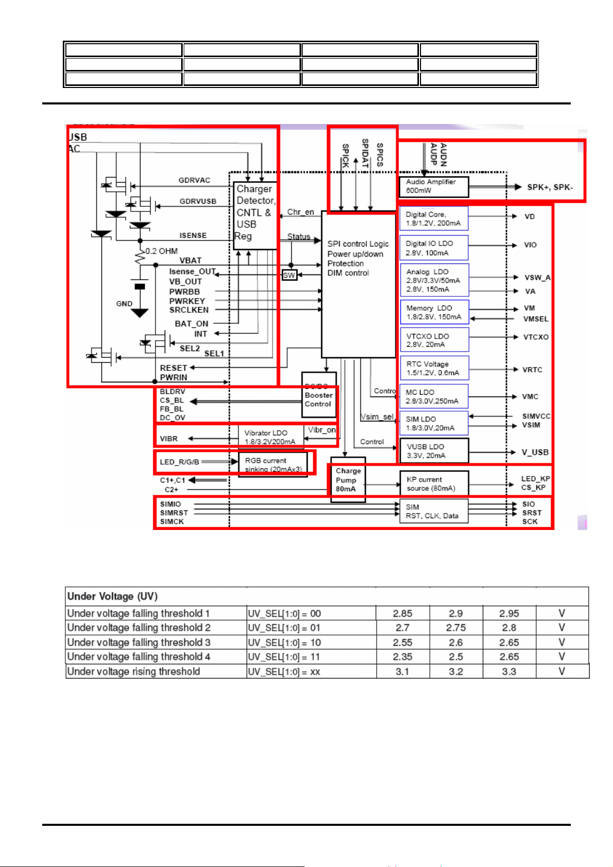
Figure 40. MT6318 Block Diagram
1.1 UV (Under Voltage)
When PWRIN < 2.9 V in the switched-on condition (active or idle). PMIC goes to the power-off state.
Mega3 is set to 2.6V. So, If incoming call or outgoing call, It is impossible to power off suddenly if Battery voltage is
lower than 3.4V.
1.2 Regulator Output
-. Charge Pump Regulator ( For keypad and RGB LED Driver)
MEGA3 TECHNICAL MANUAL Page 3.53
Page 54

MODEL MEGA3 VERSION V_1.01
PREPARED BY H/W DATE 2008.APR.23
SUBJECT TECHNICAL MANUAL PAGE 54/77
Mega3 did not use the RGB LED driver but use the Keypad Driver as shown below. The Output Current of KeyLED_A
is max 80mA and 4.5V. If Charge pump used, The C311, C312 needed for charging.
Figure 41. Keypad Charge Pump Circuit.
Slide Keypad did not use the Keypad charge pump from MT6318. The Vout_LED is a charge pump output from Rohm
BD6081GU Driver. And The LED_CS is CMOS Open drain.
1.3 Vcore (Digital Core Voltage)
MEGA3 TECHNICAL MANUAL Page 3.54
Page 55

MODEL MEGA3 VERSION V_1.01
PREPARED BY H/W DATE 2008.APR.23
SUBJECT TECHNICAL MANUAL PAGE 55/77
The digital core LDO(VD output) is a regulator that could source 200mA with 1.2V output voltage with Pin E9 low state.
If Pin E9 is high, The output Voltage is 1.8V. It supplies the baseband circuitry in the handset. MEGA3 use 1.2V .
1.4 DVDD (Digital I/O voltage)
1.5 AVDD (Analog Voltage)
The analog LDO is a regulator that could source 150mA with 2.8V output voltage. It supplies the analog sections of the
baseband chipsets. The LDO is optimized for low frequency ripple rejection in order to reject the ripple coming from the RF
Power Amplifier burst frequency at 217Hz. The Decoupling Capacitor C309 4.7uF must be higher than X5R type.
1.6 VCTCXO
The TCXO LDO is a regulator that could source 20mA with 2.8V output voltage. It supplies the temperature compensated
crystal oscillator (U201), which needs its own ultra low noise supply and very good ripple rejection ratio. The Decoupling
Capacitor C307 2.2uF must be higher than X5R type.
1.7 VRTC
The RTC LDO is a regulator that could source 200uA with 1.2V/1.5V according to Pin C9 Status. If Pin C9 is high, The
voltage is 1.5V. MEGA3 uses 1.2V. MT6318 has a 2 steps RTC Block to increase the RCT alive time. 1 step is for charging
the Backup battery by 2.8V. Another step is for supply the Voltage to VRTC by 1.5/1.2V.
Figure 42. RTC block diagram.
MEGA3 TECHNICAL MANUAL Page 3.55
Page 56

MODEL MEGA3 VERSION V_1.01
PREPARED BY H/W DATE 2008.APR.23
SUBJECT TECHNICAL MANUAL PAGE 56/77
1.8 VMEM (external memory voltage)
The memory LDO is a regulator that could source 150mA with 1.8V/2.8V output voltage selection based on the supply
specs of memory chips. It supplies the memory circuitry in the handset. If Pin K4 VMSEL is connected to GND, The VMEM
is 1.8V. MEGA3 uses 1.8V for MT6228 VDD33_EMI and SDRAM VDD,VDDQ
.
1.9 VSIM (SIM voltage)
The SIM LDO is a regulator that could source 20mA with 1.8V or 3.0V output voltage selection based on the supply specs of
subscriber identity modules card. The LDO is controlled independently of the others LDO.
1.10 VMC(Memory Card Voltage)
The VMC LDO is a regulator that could source 250mA with 2.8V or 3.0V according to D3 bit of MT6318 Register Index F.
The LDO is controlled independently of the others LDO.
1.11 KP_LED_Voltage
1.12 VUSB(USB Voltage)
1.13 VIB_3.2V (Vibrator Voltage)
The VVIB LDO is a regulator that could source 200mA with 1.8V or 3.2V output voltage according to the Register E.
MEGA3 TECHNICAL MANUAL Page 3.56
Page 57

MODEL MEGA3 VERSION V_1.01
PREPARED BY H/W DATE 2008.APR.23
SUBJECT TECHNICAL MANUAL PAGE 57/77
1.14 Charger Circuit
Rsense is 0.2mOhm. So, The Maximum charging current is 800mA. But, The Charging current can be controlled to 400, 600
and 800mA by SPI Register.
1.14.1 Power Management Status
Figure 43. Power Management Diagram.
MEGA3 TECHNICAL MANUAL Page 3.57
Page 58

MODEL MEGA3 VERSION V_1.01
PREPARED BY H/W DATE 2008.APR.23
SUBJECT TECHNICAL MANUAL PAGE 58/77
1.14.2 Charger Detector
The charger detector senses the charging voltage from either a standard AC-DC adaptor or a USB connection. When the
charging input voltage is greater than the pre-determined threshold, the charging process is triggered. This detector resists
higher input voltages than other parts of the PMIC; i.e. if an excess charging source is detected (> 9.0 V), the charger detector
stops the charging process to avoid burning out the whole chip or even the whole phone. If both AC and USB chargers are
detected, the charging source uses the AC source.
When the presence of a charger voltage (either AC or USB) is detected, an interrupt output pin INT becomes active (pull
LOW). The INT is also active when the AC or USB regulator is removed. The PMIC resets INT to HIGH after the BB chip
reads the PMIC through the SPI.
1.14.3 Control for Pre-charge indication
The PMIC provides 2 control signals SEL1 and SEL2 for the application that shows pre-charge status on the LCD. In normal
cases, VBAT is selected (SEL2 turned on) as the power input to the PMIC.
Figure 44. SEL1, SEL2 Circuit for switching Precharging/Normal charging
MEGA3 TECHNICAL MANUAL Page 3.58
Page 59

MODEL MEGA3 VERSION V_1.01
PREPARED BY H/W DATE 2008.APR.23
SUBJECT TECHNICAL MANUAL PAGE 59/77
Under battery low conditions (VBAT < 3.3 V), the AC charger source is selected (SEL1 turned o n) to substitute for the
power normally provided by VBAT, allowing the BB to power up and at least light up the LED to show the charging status.
SEL1 is turned on only in the pre-charging state, SEL1 and SEL2 must not be turned on simultaneously at any time.
During the pre-charging state, when VBAT passes 3.3 V, the PMIC switches SEL1 off and SEL2 on to have the VBAT supply
the whole system as under normal conditions. That times, The handset is reset fully.
Table 1 lists the SEL 1 and SEL 2 states for each phone state.
The threshold voltage to determine the VBAT signal is 3.3 V for pre-charge state to CC mode, and 3.0 V for
returning to pre-charge mode. This hysteresis is designed to prevent the state from bouncing back and forth between charge
modes in events such as a surge of current demanded.
1.14.4 I-V Curve for LiO+ battery
The Figure 45 shows the Charging Current VS Voltage for LiO+ Battery. As shown, The Charging mode is 4 kinds.
Pre-charging, CC Charging, CV Charging and Charging Complete according to Battery voltage.
MEGA3 TECHNICAL MANUAL Page 3.59
Page 60

MODEL MEGA3 VERSION V_1.01
PREPARED BY H/W DATE 2008.APR.23
SUBJECT TECHNICAL MANUAL PAGE 60/77
Figure 45. I-V Curve for LiO+ Battery
1.14.5 Charging Voltage Control
PMIC outputs both VBAT and ISENSE voltage to VB_OUT and ISENSE_OUT pins. In addition, the divide-by-two option
is supported. This function facilitates monitoring of the VBAT and ISENSE voltages by the BB, to control the charging
process. Baseband is reading the ADC0_I-(VBAT VBSENSE) and ADC1_I+ (Current ISENSE) per 10seconds during 0.5mS.
If battery is low (under 3.6V), Reading is per 5seconds to prevent to power off suddenly.
2. SPI
PMIC uses a 3wire interface to connect to the BB. This bi-directional serial bus interface allows the BB to write commands
to and read status from PMIC. The bus protocol employs a 16-bit proprietary format. The descriptions for the 3 signals are
listed in below Table.
When SPICS goes low, this bus is active. The BB transfers the 4 register index bits followed by a read/write bit, then
waits 3 clock cycles for the PMIC SPI state machine to decode the operation for the succeeding 8 data bits.
The state machine counts for 16 clocks to complete the data transfer. If fewer than 16 clocks are received during the
time that SPICS = 0 then only part of the data has been transferred. On the other hand, if more than 16 clocks are received, the
extra data is ignored. The first SPICK is started 100 ns after the SPICS is asserted low.
3. Register Table
The PM IC MT6318 does detect the H/W Status and Controlled by Registers with SPI Communication.
MEGA3 TECHNICAL MANUAL Page 3.60
Page 61

MODEL MEGA3 VERSION V_1.01
PREPARED BY H/W DATE 2008.APR.23
SUBJECT TECHNICAL MANUAL PAGE 61/77
4. SIM card interface
It provides level shifting needs for low voltage GSM controller to communicate with either 1.8V or 3V SIM cards.. All SIM
cards contain a clock input, a reset input, and a bi-directional data input/output. The clock and reset inputs to SIM cards are
level shifted from the supply of digital IO of baseband chipset to the SIM supply. The SIMIO, SIMRST and SIMCLK are
from Baseband. The SIO, SRST and SCLK is from MT6318 to SIM card.
MEGA3 TECHNICAL MANUAL Page 3.61
Page 62

MODEL MEGA3 VERSION V_1.01
PREPARED BY H/W DATE 2008.APR.23
SUBJECT TECHNICAL MANUAL PAGE 62/77
IV. HYC0UGE0MF1P
1024M (128Mx8bit) NAND FLASH Memory and 256M (16Mx16bit) Mobile SDRAM Multi-Chip
Package
The HYC0UGE0MF1(P)Series is suited for mobile communication system application which use in data memory to reduce
not only mount area but also power consumption. The HYNIX HYC0UGE0MF1(P) is a Multi Chip Package Memory which
combined a
SDRAM). Combination of HYC0UEE0CF1(P), 512Mbit NAND Flash memory is organized as 64M x8 bits and the size of a
Page is either 528 Bytes (512 + 16 spare) depending on whether the device has a x8 bus width. 256Mbit Low Power
SDRAM(Mobile SDRAM) is a 268,435,456bit CMOS Synchronous DynaMIC Random Access Memory. It is organized as
4banks of 4,194,304x16.
The devices are available in the following packages: 149-Ball P-FBGA Type - 10x14.0mm, 0.8mm pitch : Lead Free
1,107,296,256-bit NAND Flash Memory and a 268,435,456-bit Low Power Synchronous DRAM(Mobile
MEGA3 TECHNICAL MANUAL Page 3.62
Page 63

MODEL MEGA3 VERSION V_1.01
PREPARED BY H/W DATE 2008.APR.23
SUBJECT TECHNICAL MANUAL PAGE 63/77
NAND FLASH MEMORY 528MBIT = 528 BYTES X 32 PAGES X 4,096 BLOCKS
MEGA3 TECHNICAL MANUAL Page 3.63
Page 64

MODEL MEGA3 VERSION V_1.01
PREPARED BY H/W DATE 2008.APR.23
SUBJECT TECHNICAL MANUAL PAGE 64/77
Figure 45. NAND Flash Block diagram and Memory Cell
Organized as 4banks of 4,194,304x16
Figure 46. SDRAM Block diagram
MEGA3 TECHNICAL MANUAL Page 3.64
Page 65

MODEL MEGA3 VERSION V_1.01
PREPARED BY H/W DATE 2008.APR.23
SUBJECT TECHNICAL MANUAL PAGE 65/77
DC Operating Voltage
DC Characteristics (NAND Flash Memory). VCC : 2.5V ~ 3.0V.
DC Characteristics (Mobile SDRAM). VDD/VDDQ : 1.7 ~ 1.95V
MEGA3 TECHNICAL MANUAL Page 3.65
Page 66

MODEL MEGA3 VERSION V_1.01
PREPARED BY H/W DATE 2008.APR.23
SUBJECT TECHNICAL MANUAL PAGE 66/77
RF section
RF Section is combined with Transceiver MT6120, VCTCXO CSX-325T26, Power Amplifier Module RF3166
and Front-End Module LMSP54HA-348(9). The MEGA3 was designed for Tri-Band according to FEM, PCB
Modify and S/W Matching.
The one type is GSM850, DCS1800 an PCS1900 with LMSP54HA-349. Another type is GSM900, DCS1800 and
PCS1900 with LMSP54HA-348.
I. MT6120 (RF Transceiver IC)
MT6120 includes LNAs, two RF quadrature mixers, an integrated channel filter, programmable gain amplifiers(PGA), an IQ
demodulator for the receiver, a precision IQ modulator with offset PLL for the transmitter, two internal TX VCOs, a VCXO,
on-chip regulators, and a fully programmable sigma-delta fractional-N synthesizer with an on-chip RF VCO.
Features Receiver
- Very low IF architecture
- Quad band differential input LNAs
- Quadrature RF mixers
- Fully integrated channel filter
- More than 100 dB gain
- More than 110 dB control range
- Image-reject down conversion to baseband
Transmitter
- Precision IQ modulator
- Translation loop architecture
- Fully integrated wideband TX VCO
- Fully integrated TX loop filter
Frequency Synthesizer
- Single integrated, fully programmable fractional- N synthesizer
- Fully integrated wideband RF VCO
- Fast settling time suitable for multi-slot GPRS application
Voltage Control Crystal Oscillator (VCXO)
- 26 MHz crystal oscillator capable of supporting 13 MHz / 26 MHz output clock
- Programmable capacitor array for coarse tuning
- Internal varactor for fine tuning
Regulators
- Built-in low-noise, low-dropout (LDO) regulators
Low power consumption
QFN (Quad Flat Non-lead) Package 56-pin SMD
3-wire serial interface
MEGA3 TECHNICAL MANUAL Page 3.66
Page 67

MODEL MEGA3 VERSION V_1.01
PREPARED BY H/W DATE 2008.APR.23
SUBJECT TECHNICAL MANUAL PAGE 67/77
Figure 47. MT6120 Functional block diagram
- Recommended Operating Range
Item Symbol Min Typ Max Unit
Power Supply Voltage(VBAT) VBAT 3.1 3.6 4.6 V
Power Supply Voltage(VCCD) VCCD 2.5 2.8 3.1 V
Operating Ambient Temperature Topr -20 25 75 C
MEGA3 TECHNICAL MANUAL Page 3.67
Page 68

MODEL MEGA3 VERSION V_1.01
PREPARED BY H/W DATE 2008.APR.23
SUBJECT TECHNICAL MANUAL PAGE 68/77
A description of MT612X hardware control pins and their functionality are shown in the table below. MT612X has an
internal VCXO and its control.
Pin Description
MEGA3 TECHNICAL MANUAL Page 3.68
Page 69

MODEL MEGA3 VERSION V_1.01
PREPARED BY H/W DATE 2008.APR.23
SUBJECT TECHNICAL MANUAL PAGE 69/77
1. Receiver
The receiver section of MT6120 includes Quad-band low noise amplifiers(LNAs), RF quadrature mixers, an onchip channel filter, Programmable Gain Amplifiers(PGAs), quadrature second mixers, and a final low-pass filter.
The very low-IF MT6120 uses image-rejection mixers and filters to eliminate interference. With accurate RF
quadrature signal generation and mixer matching techniques, the image rejection of the MT6120 can reach 35dB
for all bands. Compared to a direct conversion receiver(DCR), MT6120’s very low-IF architecture improves the
blocking rejection, AM suppression, as well as the adjacent channel interference performance.
- Receiver Input Frequency
Mode Min Max Unit
GSM850 869 894 Mhz
GSM900 925 960 Mhz
MEGA3 TECHNICAL MANUAL Page 3.69
Page 70

MODEL MEGA3 VERSION V_1.01
PREPARED BY H/W DATE 2008.APR.23
SUBJECT TECHNICAL MANUAL PAGE 70/77
DCS 1805 1880 Mhz
PCS 1930 1990 Mhz
The below table is shown LNA input impedance. So, From FEM Sawfilter to MT6120 LNA input, The
Impedance matching is need for high sensitivity. The L903,L904,L905, C910,C911,C912,C913,C914 and C915
are the matching State.
The IF signal is then filtered and amplified through an image-rejection filter and a PGA. The multi-stage PGA is implemented
between filtering stages to control the gain of the receiver. With 2 dB gain steps, a 78 dB dynaMIC range of the PGA ensures
a proper signal level for demodulation. The quadrature 2
in an analog differential IQ format.
nd
mixers are provided on-chip to down convert IF signal to baseband
2. Transmitter
The MT6120 transmitter section consists of two on-chip TX VCOs, buffer amplifiers, a down-converting mixer, a
quadrature modulator, an analog phase detector and a digital phase frequency detector, each with a charge pump
output and on chip loop filter. The dividers and loop filters are used to achieve the desired IF frequency from the
down-conversion mixer and quadrature modulator. For a given transmission channel, the transmitter will select one
of the two different TX reference dividing numbers. These built-in components, along with an internal voltage
controlled oscillator and a loop filter, implement a translation loop modulator. The TX VCO output is fed to the
power amplifier. A control loop, implemented externally, is used to control the PA’s output power level.
- Transceiver Output Frequency
Mode Min Max Unit
GSM850 824 849 Mhz
GSM900 880 915 Mhz
DCS 1710 1785 Mhz
PCS 1850 1910 Mhz
3. TX VCO
MEGA3 TECHNICAL MANUAL Page 3.70
Page 71

MODEL MEGA3 VERSION V_1.01
PREPARED BY H/W DATE 2008.APR.23
SUBJECT TECHNICAL MANUAL PAGE 71/77
Two power VCOs are integrated with OPLL to form a complete transmitter circuit. The TX VCO output power is
typically 9dBm with +/-2.5dB variation in GSM850 bands and +8dBm output power with +/-2dB variation in
PCS1900 bands over extreme Temperature conditions.
The PAM(RF3166) Input range is typically 3dBm. So 5dB Attenuator is added Between MT6120 and RF3166.
- For GSM850/GSM900 : R406, R407, R408,
- For DCS/PCS : R403, R404, R405.
TX VCO Frequency Range is same with Transmitter Frequency Range.
4. Frequency Synthesizer
The MT6120 includes a frequency synthesizer with a fully integrated RF VCO to generate RX and TX local
oscillator frequencies. The PLL locks the RF VCO to a precision reference frequency at 26MHz. To reduce the
acquisition time or to enable fast settling time for multi-slot data services such as GPRS, a digital loop along with a
fast-acquisition system are implemented in the synthesizer. After the calibration, a fast-acquisition system is
utilized for a period of time to facilitate fast locking.
The frequency ranges of the synthesizer for RX mode are
RX mode GSM850 1737Mhz ~ 1788Mhz
GSM900 1850Mhz ~ 1920Mhz
DCS1800 1805Mhz ~ 1880Mhz
PCS1900 1930Mhz ~1990Mhz
The Calculate LO Frequency Fvco from RX Channel Frequency Fch is following.
Fvco = 2*Fch-200K for GSM850 and GSM900
Fvco = Fch-100K for DCS1800 and PCS1900.
The frequency ranges of the synthesizer for TX mode are
TX mode GSM850 1813Mhz ~ 1868Mhz
GSM900 1936Mhz ~ 2059Mhz
DCS1800 1881Mhz ~ 2008Mhz
PCS1900 2035Mhz ~2149Mhz
The Calculate LO Frequency Fvco from TX Channel Frequency Fch is following.
(Set the divider ratio D1 of TX reference divider = 11)
Fvco = 2*D1*Fch/(D1-1) for GSM850 and GSM900
Fvco = D1*Fch/(D1-1) for DCS1800 and PCS1900.
The MT6120 uses a digital calibration technique to reduce the PLL settling time once the RF synthesizer is
programmed through a 3-wire serial interface, the calibration loop is activated. The main function of the calibration
loop is to preset the RF VCO to the vicinity of the desired frequency quickly and correctly, thus aiding the PLL to
MEGA3 TECHNICAL MANUAL Page 3.71
Page 72

MODEL MEGA3 VERSION V_1.01
PREPARED BY H/W DATE 2008.APR.23
SUBJECT TECHNICAL MANUAL PAGE 72/77
settle faster. On the other hand, since a large portion of initial frequency error is dealt with by the integrated
calibration loop, the overall locking time can be drastically reduced, irrespective of the desired frequency.
5. Voltage Control Crystal Oscillator(VCXO)
VCXO consists of an amplifier, a buffer, and a programmable capacitor array. The VCXO provides the MT6120
with a selectable reference frequency of either 13MHz or 26MHz. When VCXOFRQ pin is high, Output Frequency
is 26Mhz. When VCXOFRQ pin is low, Output Frequency is 13Mhz.
VCXOFRQ is high in MEGA3. The Amplifier is designed to be in series resonance with a standard 26Mhz crystal.
The Crystal is connected from the Input pin XAL of Amplifier to ground through a series load capacitance. The
buffer provides a typical 600mVpp voltage swing. As an alternative, the reference frequency can be provided by
an external 26Mhz VCTCXO module. When Pin VCXOCXR is tied to the VCCVCXO supply, the XTAL pin will
accept an external signal. Furthermore, the VCXO control pin can be tied to VCCVCXO to prevent the current
leakage during the sleep mode operation.
6. Regulator
The MT6120 internal regulators provide low noise, stable, temperature and process independent supply voltages to
critical blocks in the transceiver. An internal P-channel MOSFET pass transistor is used to achieve a low dropout
voltage of less than 150mV in all regulators.
II. RF3166 ( GSM850,GSM900 and DCS,PCS Power
Amplifier Module)
MEGA3 TECHNICAL MANUAL Page 3.72
Page 73

MODEL MEGA3 VERSION V_1.01
PREPARED BY H/W DATE 2008.APR.23
SUBJECT TECHNICAL MANUAL PAGE 73/77
Figure 48. RF3166 Block Diagram
The RF3166 is a high-power, high-efficiency power amplifier module with integrated power control that provides
over 50dB of control range. The device is a self-contained6mmx6mm module with 50Ω input and output terminals.
The device is designed for use as the final RF amplifier inGSM850, EGSM900, DCS and PCS handheld digital
cellular equipment and other applications in the 824MHz to849MHz, 880MHz to 915MHz, 1710MHz to
1785MHzand 1850MHz to 1910MHz bands. The RF3166 incorporates RFMD’s latest VBATT tracking circuit,
which monitors battery voltage and prevents the power control loop from reaching saturation. The VBATT tracking
circuit eliminates the need to monitor battery voltage, thereby minimizing switching transients. The RF3166
requires no external routing or external components, simplifying layout and reducing board space.
The VRamp Range is from 0.26V to 2.1V. And the R400, R401, C408 is a Voltage divider for fine tuning and
Low pass filter of 300Khz.
The Input/Output Impedance is 50ohm. So, The PCB Design must be designed with 50ohm strobe line.
Thermal vias are required in the PCB layout to effectively conduct heat away from the package. The via pattern
has been designed to address thermal, power dissipation and electrical requirements of the device as well as
accommodating routing strategies. The via pattern used for the RFMD qualification is based on thru-hole vias with
0.203mm to 0.330mm finished hole size on a 0.5mm to 1.2mm grid pattern with 0.025mm plating on via walls. If
MICro vias are used in a design, it is suggested that the quantity of vias be increased by a 4:1 ratio to achieve
similar results.
MEGA3 TECHNICAL MANUAL Page 3.73
Page 74

MODEL MEGA3 VERSION V_1.01
PREPARED BY H/W DATE 2008.APR.23
SUBJECT TECHNICAL MANUAL PAGE 74/77
Figure 49. Power control sequence
MEGA3 TECHNICAL MANUAL Page 3.74
Page 75

MODEL MEGA3 VERSION V_1.01
PREPARED BY H/W DATE 2008.APR.23
SUBJECT TECHNICAL MANUAL PAGE 75/77
The Next Picture is for RF TX Timing of BSI and BPI.
< Single Slot TX Event with Timing Requirement>
<BSI Interface>
In order to simply the serial control mechanism, and achieve best usage of BSI resources. Each burst transmitted,
There are three generic timing defined (ST1/ST2/ST3) to send 3-wire control commands to transceiver. Usually
1’st BSI event(ST1) is used to warm up the synthesizer and set its N-counter to lock the operational frequency. The
2’nd BSI(ST2) is used to set the transmitted mode and indicate the operational band. The 3’rd BSI(ST3)is used to
command transceiver entering idle mode. All bands(GSM/DCS/PCS) share the same timing.
<BPI interface>
In order to simply the parallel control mechanism, and achieve best usage of BPI resources. Each burst transmitted,
there are also three generic timing defined(PT1/PT2/PT3) to send HW control Signals to RF module. In other
words, there are only three timing events to trigger HW control signals changing their states. Usually 1’st BPI
event(PT1) is used to select suitable band for TXVCO. The 2’nd BPI(PT2) is used to turn on PA and control
antenna switch depends on its band. The 3’rd BSI(ST3) is used to force RF module to terminate transmission and
enter idle mode. All bands share the same timing but could has different HW control signals.
MEGA3 TECHNICAL MANUAL Page 3.75
Page 76

MODEL MEGA3 VERSION V_1.01
PREPARED BY H/W DATE 2008.APR.23
SUBJECT TECHNICAL MANUAL PAGE 76/77
III. LMSP54HA-348 (Antenna Switch Module
For Tri- Band with SAW Filter)
LMSP54HA-348 is an Antenna Switch Module for GSM900, DCS1800 and PCS1900 of Murata with Three SAW
Modules. Control Pins (VC1, VC2, and VC3) are connected to LB_TX, HB_TX, and PCS_RX (signals from
baseband processor). The Control Pins Operating range is 2.4V ~ 2.8V.
LB_TX : GSM900 TX Enable.
HB_TX : DCS1800, PCS1900 TX Enable.
PCS_RX : PCS RX Enable.
Figure 50. The Evaluation board of LMSP54HA-348
MEGA3 TECHNICAL MANUAL Page 3.76
Page 77

MODEL MEGA3 VERSION V_1.01
PREPARED BY H/W DATE 2008.APR.23
SUBJECT TECHNICAL MANUAL PAGE 77/77
The GSM900 and DCS1800/PCS1900 input port matching impedances are 50 ohm from PAM(RF3166).
The GSM900, DCS1800 and PCS1900(Balance) output port matching impedance are 150ohm to Transceiver
(MT6120).
The Next Picture is for RF Receiving Timing of BSI and BPI.
<Single Slot RX Event with Timing Requirement>
<BSI Interface>
In order to simply the serial control mechanism, and achieve best usage of BSI resources. Each burst received, there
are three generic timing defined (SR1/SR2/SR3) to send 3-wire control commands to transceiver. Usually 1’st BSI
event(SR1) is used to warm up the synthesizer and set its N-Counter to lock the operation frequency. The 2’nd
BSI(SR2) is used to set the receiving amplifier gain, received mode and operation band of transceiver. The 3’rd
BSI(SR3) is used to command transceiver entering idle mode. All bands(GSM/DCS/PCS) share the same timing.
<BPI Interface>
In order to simply the parallel control mechanism, and achieve best usage of BPI resources. Each burst received,
there are also three generic timing defined(PR1/PR2/PR3) to send HW Control signals to RF Module. In other
words, There are only three timing events to trigger HW control signals changing its state. Usually 1’st BPS
event(PR1) is used to activate the RF Component. The 2’nd BPI(PR2) is used to control antenna switch depend on
its band. The 2’rd BPI(PR3) is used to force RF Module entering idle mode. All bands(GSM/DCS/PCS) share the
same timing but could have different HW control signals.
MEGA3 TECHNICAL MANUAL Page 3.77
 Loading...