

Page 1

Service Manual
1 / 31
Page 2

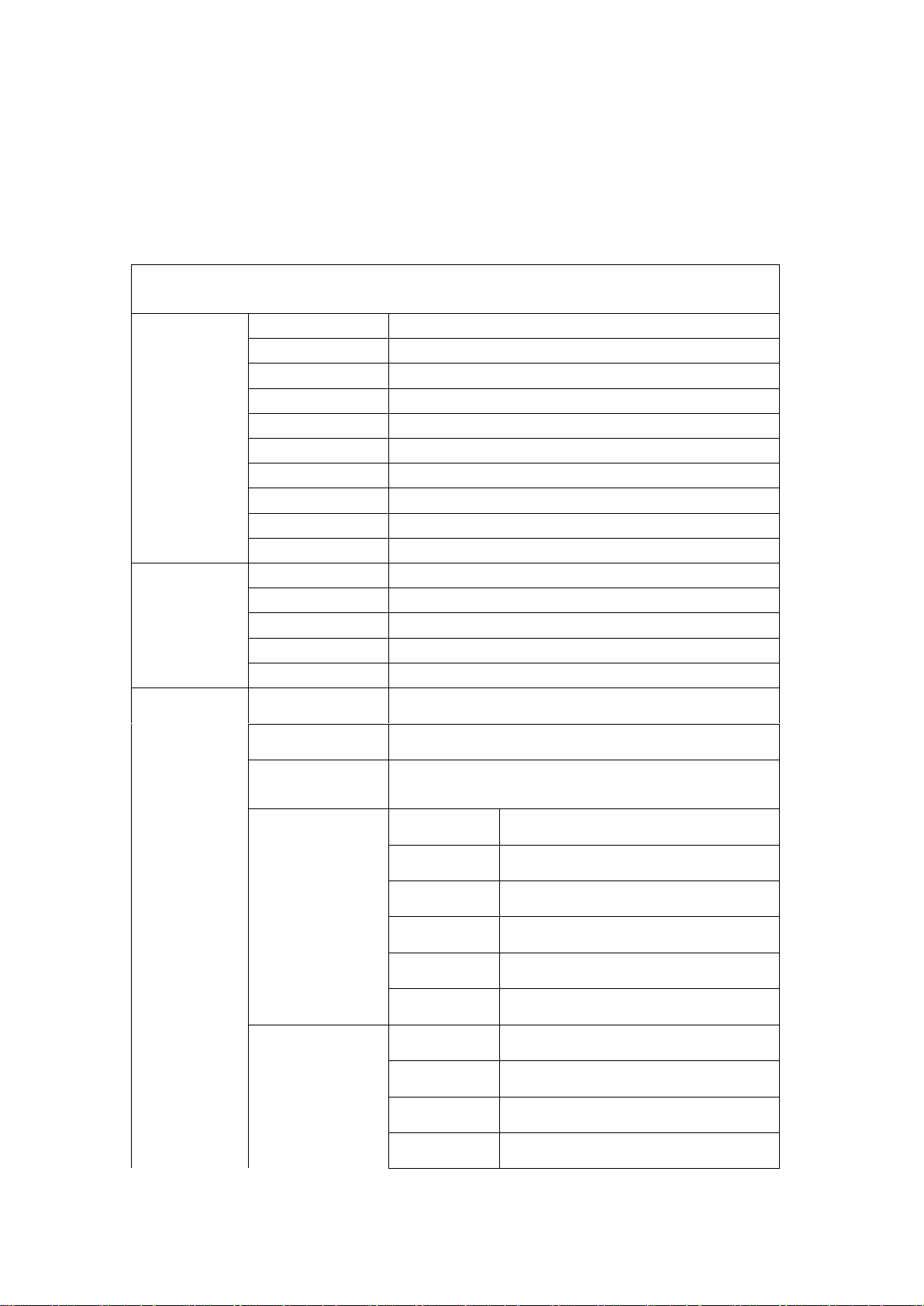
CONTENT
1 OUTLINE ................................................................................................................................................. 3
1.1 MOBILE PHONE INTRODUCTION..................................................................................................... 3
1.2 MOTHERBOARD COMPONENTS DISTRIBUTION ........................................................................................... 6
2 SIGNAL FLOW AND FAULT ANALYSIS ...................................................................................................... 7
2.1 RF PART ............................................................................................................................................ 7
2.1.1 Block Diagram of the RF Section ............................................................................................. 7
2.1.2 Signal Flow OF the RF Transmitting Part.................................................................................. 7
2.1.2.1 Receiving and Transmit Path ............................................................................................ 7
2.1.2.2 Maintenance Procedures of the Transmitting Part .......................................................... 9
2.1.3 Signal Flow of the Receiving Part .......................................................................................... 10
2.1.3.1 Receiving Part Components ........................................................................................... 10
2.1.3.2 Maintenance Procedures of the Receiving Part ........................................................ 10
2.2 BASEBAND PART ................................................................................................................................ 12
2.2.1 Block Diagram of the Baseband Part ..................................................................................... 12
2.2.2 Power Management Part ...................................................................................................... 13
2.2.2.1 The Whole Power Supply System ................................................................................... 14
2.2.3 Audio Part .............................................................................................................................. 15
2.2.3.1 Audio CODEC Circuit ...................................................................................................... 15
2.2.3.2 MIC, RECEIVER LOOP ...................................................................................................... 16
2.2.3.3 HEADSET LOOP ............................................................................................................... 17
2.2.4 BASEBAND FAUIT ISSUES ....................................................................................................... 18
2.2.4.1 Analysis of the Keyboard Fault ....................................................................................... 18
2.2.4.2 Analysis of the Display Module Circle ............................................................................ 19
2.2.4.3 FM Module ..................................................................................................................... 20
2.2.4.4 Camera Module.............................................................................................................. 21
2.2.4.5 IO Interface .................................................................................................................... 22
2.2.4.6 SIM Card Circuit ............................................................................................................. 22
2.2.4.7 T-FLASH Card Circuit ..................................................................................................... 23
2.2.4.8 BT Circuit ....................................................................................................................... 23
2.2.4.9 WIFI Circuit .................................................................................................................... 24
2.2.4.10 GPS Circuit ................................................................................................................... 25
2.2.4.11 M-sensor Circuit .......................................................................................................... 26
2.2.4.12 G-sensor Circuit ........................................................................................................... 26
2.2.4.13 IR-sensor Circuit .......................................................................................................... 27
2 / 31
Page 3
1 Outline
Product Hardware Introduction
Base Chip Set
BB
MT6582V/X
PMIC
MT6323GA
Transceiver
MT6166
Camera DSP/MMP
NA
RFPA
SKY77590-11
FM
MT6627
BT
MT6627
Audio CODEC&PA
-
Memory
Samsung
TP IC
GT915
Peripheral
Configuration
LCD
-
Backlight Driver
RT8514
CAMERA
OV8830
Memory Card
TF Card
Antenna
monopole
Basic
Performance
Indicators
Leakage current
≤ 150uA
Standby current
≤ 7mA
Call current as
maximum power
TBD
Board-level power
EGSM
32.5dBm
GSM850
32.5 dBm
DCS
29.5dbm
PCS
29.5dbm
Band1
23dbm
Band8
23dbm
Board-level
receiver sensitivity
EGSM
-108dbm
GSM850
-108 dbm
DCS
-108 dbm
PCS
-108 dbm
1.1 MOBILE PHONE INTRODUCTION
3 / 31
Page 4

Band 1
-109.5 dbm
Band 8
-109.5 dbm
TRP
EGSM
28.8dbm
GSM850
27.0 dbm
DCS
28.0dbm
PCS
28.0dbm
Band 1
20.0dbm
Band 8
20.0dbm
TIS
EGSM
-105dbm
GSM850
-105dbm
DCS
-106dbm
PCS
-106dbm
Band 1
-107dbm
Band 8
-107dbm
4 / 31
Page 5
CPU
MT6582V/X
PMIC
MT6323GA
BATTRY
CAMERA
FM、BT、
WiFi、GPS
LCD:854*480
KEYPAD
T-FLASH
MEMORY
MT6166
SKY77590
-11
SPK
HP
REC
DUAL SIM
CARD
MIC
CTP
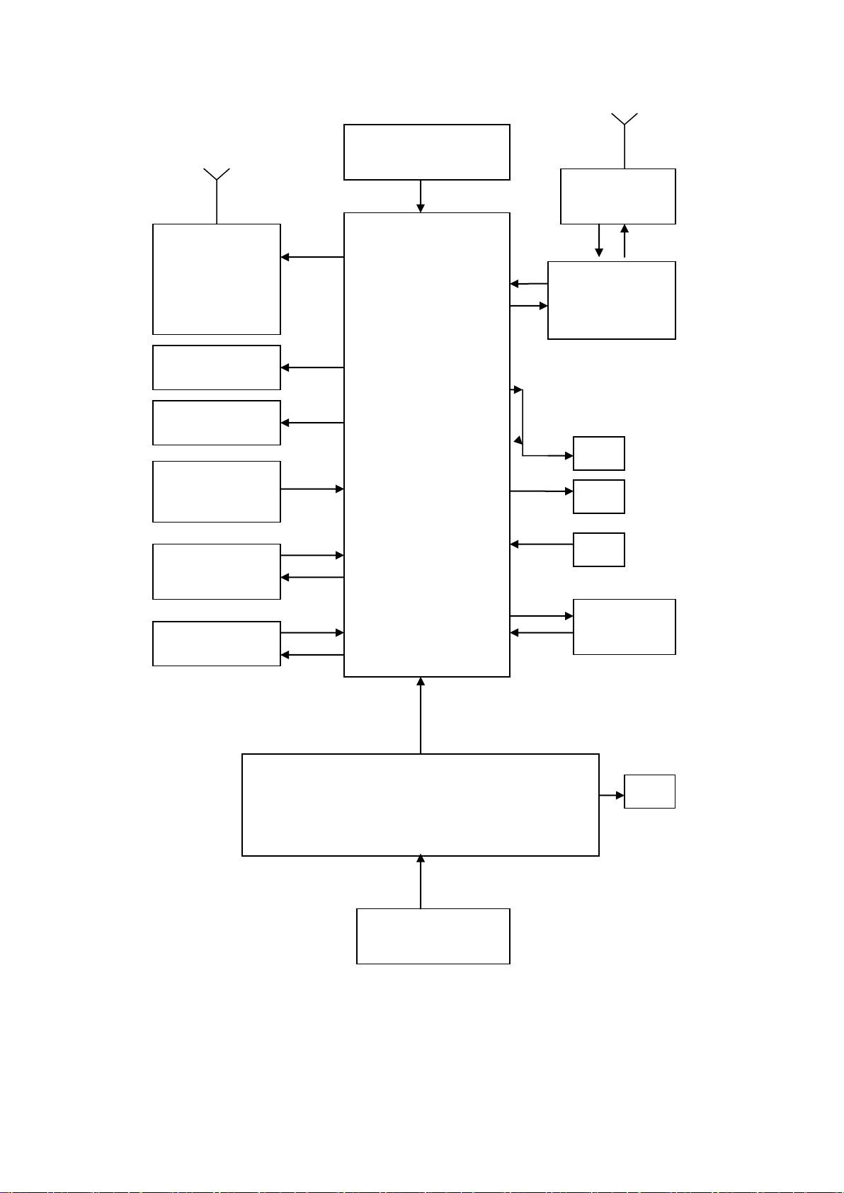
System Block Diagram
5 / 31
Page 6
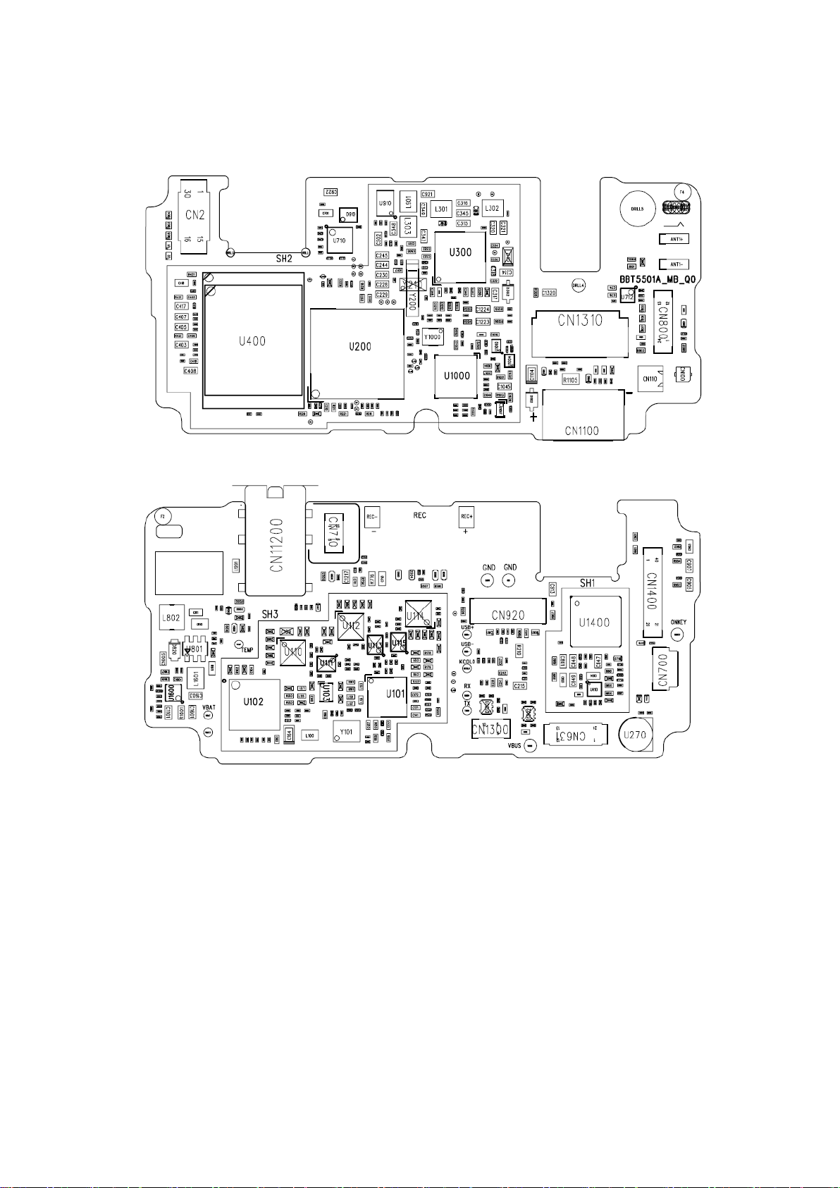
1.2 Motherboard Components Distribution
6 / 31
Page 7
2 Signal Flow And Fault Analysis
A
N
T
PA &
Ant Switch
SKY77590
-11
Transceiver
MT6166
CPU
MT6582V/
X
MT6582V/X
MT6166
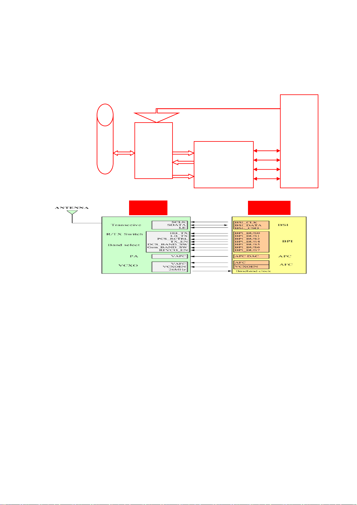
2.1 RF Part
2.1.1 Block Diagram of the RF Section
RF Diagram
GSM RF and BB interface diagram
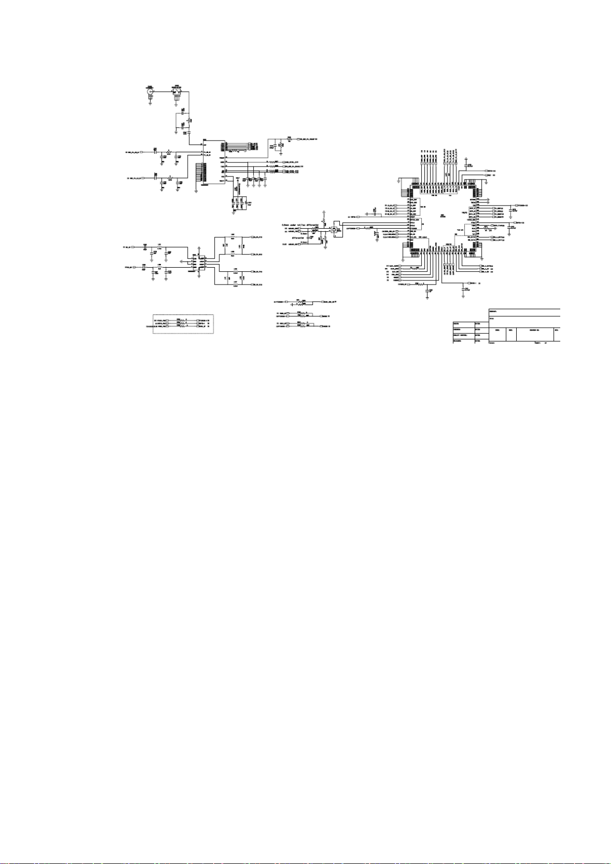
2.1.2 Signal Flow OF the RF Transmitting Part
2.1.2.1 Receiving and Transmit Path
Receiving
7 / 31
Page 8
8 / 31
Page 9
2.1.2.2 Maintenance Procedures of the Transmitting Part
(NO launch) Connect the PC and the phone with maintenance line,
then making the phone into the RF state with META software
Check Transceiver to see
if IO signals exist.
Check the PA output to
see if there is RF signal in
Y
Check CPU
N
Check RF coaxial
switch or matching
network.
Y
Check the Transceiver
to see if there is RF
signal output.
N
CheckVBAT,PA_EN,B
ANDSW_DCS,VAPC
Replace PA
Y
Check CPU
Y
Check Transceiver if LE、
SCLK/SDAT、RFVCOEN、
VCXOEN have the
correct signal.
N N
N
Y
Replace Transceiver
9 / 31
Page 10
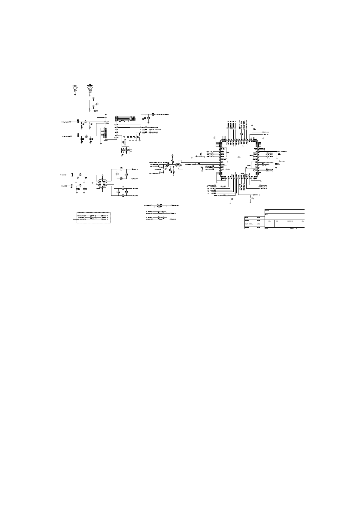
2.1.3 Signal Flow of the Receiving Part
2.1.3.1 Receiving Part Components
2.1.3.2 Maintenance Procedures of the Receiving Part
10 / 31
Page 11

11 / 31
No receiving
Start the META software to connect the PC and the phone,making the phone into the receiving state.
Signal generator is also adjusted to the correspond CH. And signal lines connected to the phone.
Transceiver has IQ?
Check CPU
Y
Transceiver has received signal?
?
N
Transceiver
CSO,SCLK,SDATA are correct ?
Check CPU
N
Whether the voltage of
the transceiver is
normal? Whether
26MHZ is normal?
Y
Check the
corresponding power
supply and 26MHZ
resulting circuit
N
Replace transceiver
Y
PA has received
signal?
N
Check to see if there has
signal in the matching circuit
between PA and ANT
N
Check to see if there has
signal in the matching
circuit between PA and
transceiver
Y
Y
Page 12

2.2 Baseband Part
2.2.1 Block Diagram of the Baseband Part
12 / 31
Page 13

CPU
MT6582V/X
PMIC
MT6323GA
BATTRY
CAMERA
FM、BT、
WiFi、GPS
LCD:800*480
KEYPAD
T-FLASH
MEMORY
MT6166
SY77590-11
SPK
HP
REC
DUAL SIM
CARD
MIC
CTP
2.2.2 Power Management Part
The power management Part use the special PMU IC : MT6323. Support 5-ways of DC-DC
13 / 31
Page 14

and 21-ways of LDO output, with AB/D, 0.7W Audio amplifier, LCD backlight driving and
Lithium battery charging circuit Inside it. Which support 5 LEDs in parallel and 10 LEDs in
series.
2.2.2.1 The Whole Power Supply System
DC-DC:
LDO
14 / 31
Page 15

2.2.3 Audio Part
2.2.3.1 Audio CODEC Circuit
Use AW8145 for audio PA
15 / 31
Page 16

2.2.3.2 MIC, RECEIVER LOOP
MIC Audio channel is shown below: This product uses the dual(OPTION)analog MIC in order to
reduce noise when you use voice calling. The power supply voltage is 1.8V-3.3V. When MIC is in
good condition but loop MIC has no echo, then you need to check the basic bias voltage signal of
the VMC, the language signals of the RECEIVER and MIC also need to be checked.
Receiver:
16 / 31
Page 17

2.2.3.3 HEADSET LOOP
Headset loop includes two signals: Headset speaker and MIC, the jack is SMT in the main-board.
If the Headset speaker has no sound、the MIC is invalid. All this need to check the SMT of the
J402
17 / 31
Page 18

2.2.4 BASEBAND FAUIT ISSUES
Download Fail
Check to see if it is caused by other
factors such as: configuration,
download cable, power supply,
Exclude the reason of
download failure
caused by other
Yes
Check to see if the serial ports between
pc and cell phone is smooth
Check if the system
connector is poor
soldered or damaged.
NO
NO
Check the resistance,
capacitance and the
EDC devices between
the system connector
and the CPU.
NO
Connect the download cable then
observe the Ammeter to see if it
shows high current(The normal
current generally about 30mA)
Yes
Quickly disconnect the
connection, and gently
touch the chip to see if it is
hot. If not, then focus point
using the multi-meter to
measure the short circuit.
Yes
Check the power manager and open the
LDO to see if the voltage supply is
normal and whether there is power
supply circuit open.
Little or no current
Check VCORE、VDD、VADD、VTCXO、VRTC、
VMEM、Measure the clock signal of 26MHZ、
32KHZ.
Current normal but download fail
Check CPU and NAND FLASH、SDRAM to see
if they are OK and the LDO is normal.
Maintenance process of the download failure Issues:
2.2.4.1 Analysis of the Keyboard Fault
This board includes 3 side-buttons. All the keyboard circuits use the scanning method to detect
except the power button, volume up and down. The scanning signal will be triggered when a
button is pressed,, then the corresponding row and column will be detected, the function of the
key can be identified according to the software definition.
18 / 31
Page 19

a. The cell phone can power on ,but all the keys are invalid.
In general, this situation is caused by some key short-circuit, the equivalent of a long
pressing this button.
At this point ,you should analyze the following first:
⑴ Check peripheral TVS of the button to see if they are short-circuit.
⑵ Then ,check the connector to see whether it is short-circuit when it is welded.
b. Failure of a single button
This situation needs to check whether the beneath of the DOME key is dirty. If the
problem is still existed, you have to check whether the circuit is open.
c. Failure of a few buttons
This situation is usually caused by a short-circuit row or column. Checking the
interface circuit to see if it has open weld phenomena and detect the disconnected
phenomena of the resistance.
2.2.4.2 Analysis of the Display Module Circle
Display module use the 4.3" LCD, which including 2 pairs MIPI differential bus mode. All of
commend and data go through the MIPI differential bus mode except the reset signal.
19 / 31
Page 20

For the screen problem you should first use the alternative method to search out whether the
problem is in the motherboard or the LCD. Focus on examining the LCM connector and EMI filter
welding.. The backlight signal is completed by the LED driver chip AW9910STR. Generally,
measure the input voltage VBAT and the enable control signal.
2.2.4.3 FM Module
The WIFI Circle is based on chip MT6627, comes with FM module and transmitter function, also
with both analog and digital audio channels choose from. The RF part supply short antenna
design and long antenna design.
The FM interface Circle as shown below:
FM use the headphone ground as the antenna,therefore the headset ground and the
motherboard ground have1000@100M magnetic beads to isolate FM(80M~108M)signals.
20 / 31
Page 21

2.2.4.4 Camera Module
The module uses 5 million pixel AF camera as the main camera, 0.3 million pixel camera as the
sub camera. Through the connector and the baseband chip (the main camera series EMI devices)
directly connected.
The Camera Interface Circuit as show below:
The Camera Power Supply Circuit
The VCAM_IOPMU supply 1.8V to Camera IO interface voltage, VCAMA_PMU supply 2.8V analog
21 / 31
Page 22

voltage.
2.2.4.5 IO Interface
2.2.4.6 SIM Card Circuit
Switch of dual SIM cards is integrated into baseband, which supports dual SIM Card function,
SIM1 support GSM/WCDMA Card, SIM2 support only GSM Card.. As show below:
22 / 31
Page 23

2.2.4.7 T-FLASH Card Circuit
The T-FLASH Card Circle support data exchange between Phone and PC. The Circuit have four
serial data transmission lines ( MCODA0,MCODA1,MCODA2,MCODA3 ) and state
detection(MCOCMD),CLOCK(MCOCK),as the show below:
2.2.4.8 BT Circuit
The Bluetooth function is one part of the MT6627 .The BT Circuit include baseband, RF unit,
UART2 unit, PCM interface system configuration, and also.
23 / 31
Page 24

2.2.4.9 WIFI Circuit
The WIFI Circuit integrated in MTK6627, The WIFI Circuit includes baseband, RF unit, power,
SDIO interface system configuration. It supports 2.4G, following 802.11b/n/g agreement,
supports safety format is WFA, WPA/WPA2, WPS2.0, WAPI.
The WIFI’S RF interface is connected with external antenna. The ANT is transmitting or receiving
signals to communicate with WIFI equipment.
24 / 31
Page 25

2.2.4.10 GPS Circuit
The GPS Circuit integrated in MTK6627, It includes baseband, RF unit, power, UART interface
system configuration. Its sensitivity supports 165dBm, supports AGPS.
The GPS’S RF interface is connected with external antenna. The ANT is receiving GPS satellite
signal to achieve positioning. GPS and BT share the same ANT. We switch GPS signal by the
switch U904, then through a narrowband filter U903(OPTION) into GPS chip.
25 / 31
Page 26

2.2.4.11 M-sensor Circuit
M-SENSOR is a electronic compass, it supports X, Y, Z three-axis orientation sensor. M-SENSOR
uses I2C to connect CPU interface, in order to transmit directives and data.
2.2.4.12 G-sensor Circuit
G-SENSOR is a sensor of acceleration due to gravity. It supports X, Y, Z three-axis orientation
sensor. M-SENSOR uses I2C to connect CPU interface, in order to transmit directives and data.
26 / 31
Page 27

2.2.4.13 IR-sensor Circuit
IR-SENSOR is light &distance sensor. It induces current phone the environment in which of the
brightness and Perceived distance of the human face in the phone calling and the phone.
IR-SENSOR uses I2C to connect CPU interface, in order to transmit directives and data, also we
need an INT give CPU a trigger signal.
27 / 31
Page 28

3. Disassembly and assembly service Tools
28 / 31
Page 29

29 / 31
Page 30

30 / 31
Page 31

31 / 31
 Loading...