

Page 1
FS554 Service_Manual
Contents
1.Overview
1.1 FS554- brief introduction................................................................................................. 2
1.2 Function diagram ............................................................................................................... 3
1.3 Mainboard component distribution diagram ...................................................................... 3
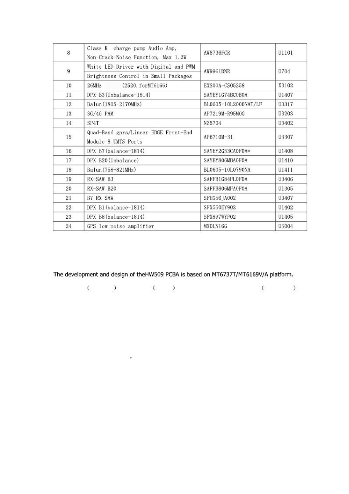
1.4 Main IC Names .................................................................................................................. 4
2. RF................................................................................................................................................. 5
2.1 RF Overview ...................................................................................................................... 5
2.2 RF circuit description......................................................................................................... 5
2.3 WiFi/BT/GPS Part.............................................................................................................. 9
3. Baseband section.......................................................................................................................... 9
3.1 Outline................................................................................................................................ 9
.......................................................... 12
3.2.1 Power failure Check.............................................................................................. 12
3.2.2 Audio faults ........................................................................................................... 13
3.2.4 LCD Fault ............................................................................................................. 16
3.2.5 FM......................................................................................................................... 18
3.2.5 Bluetooth............................................................................................................... 19
3.2.6 WIFI fault.............................................................................................................. 19
3.2.6 Camera fault .......................................................................................................... 20
3.2.7 SIM card failure .................................................................................................... 21
3.2.8 Motor test is invalid .............................................................................................. 22
3.2.9 Gravity Sensor....................................................................................................... 23
3.2.10 T-Flash fault ........................................................................................................ 24
3.2.11Touch Panel function............................................................................................ 25
3.2.13 Cannot boot failure.............................................................................................. 26
1
Page 2
1. FS554- overview
1.1 FS554- brief introduction
FS554-
2
Page 3
1.2 Function diagram
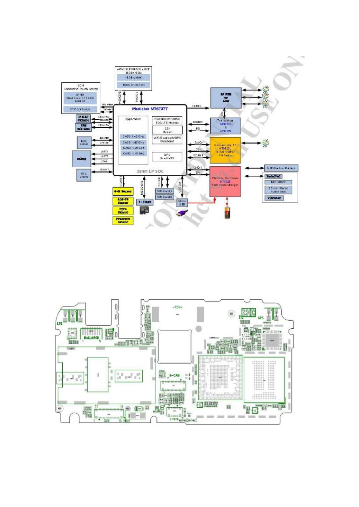
1.3 Mainboard component distribution diagram
Mainboard TOP
3
Page 4
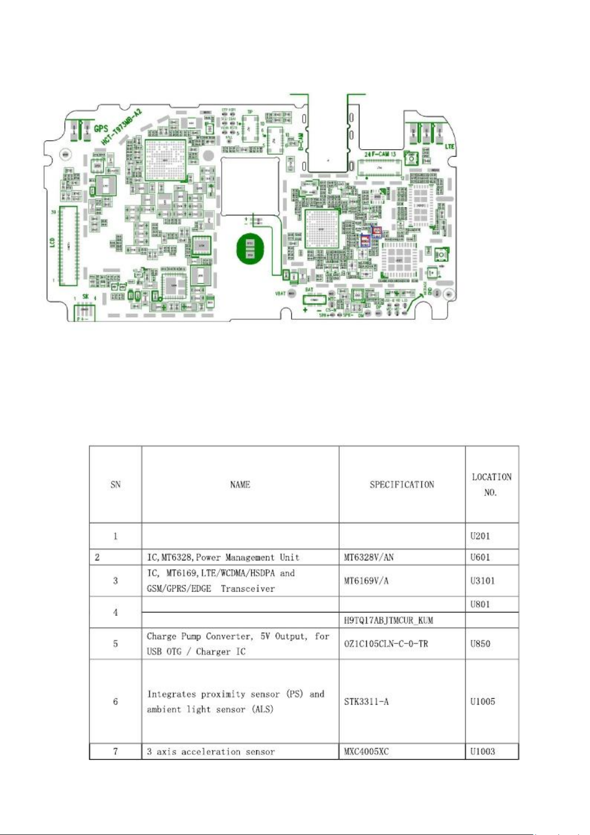
Mainboard BOTTOM
1.4 Main IC Names
MTK_6737T
Baseband Chip
MT6737V/WT
eMMC+LPDDR3(16GB+16Gb,1.8/1.2V) KMQE10013M-B318007
eMMC+LPDDR3(16GB+16Gb)
4
Page 5
crystal
2. RF
2.1 RF Overview
a TWO-band 900/1800 and two-band B1/B8 WCDMA/HSPA and Three-band B3/B7/B20
FDD mobile phone. The transmitter operates in a half-duplex for GSM and full-duplex for
WCDMA/HSDPA and FDD.
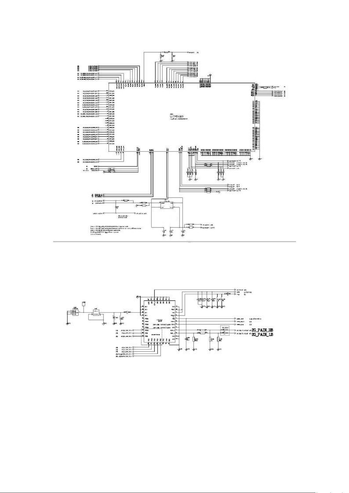
The majority of the phone circuitry consists: the MT6737V/WT Application and Modem
Processor,MT6328V power manage IC,MT6169 RF Transceiver , GSM Ant: AIROHA
AP6710M-31 Antenna switch and AIROHA PAAP7219M-R95MOG for
Band3/Band7/Band20/DCS1800/PCS1900/GSM850/EGSM900. The Diversity Antenna: Nationz
NZ5704 Antenna switch. And MT6625LN/A for GPS/ WIFI/BT/FM radio.
2.2 RF circuit description
2.2.1 The circuit description of receiving part
5
Page 6
RF transceiver receiving ports
LTE PRX Antenna switch And 2G PA
6
Page 7

LTE DRX Antenna port
2.2.2 The circuit description of transmitting part
WCDMA Band1 Duplexer
WCDMA Band8 Duplexer
7
Page 8
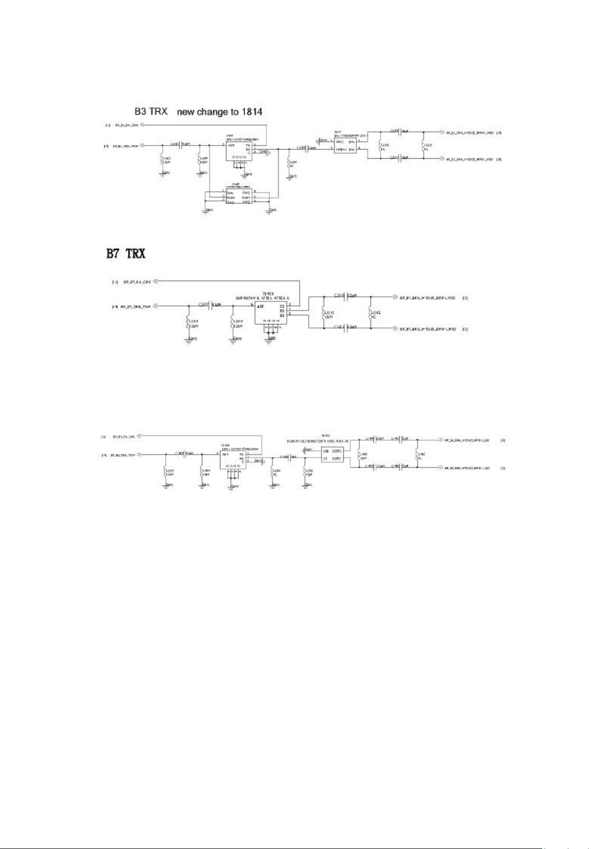
LTE Band3 Duplexer
LTE Band7 Duplexer
LTE Band20Duplexer
8
Page 9
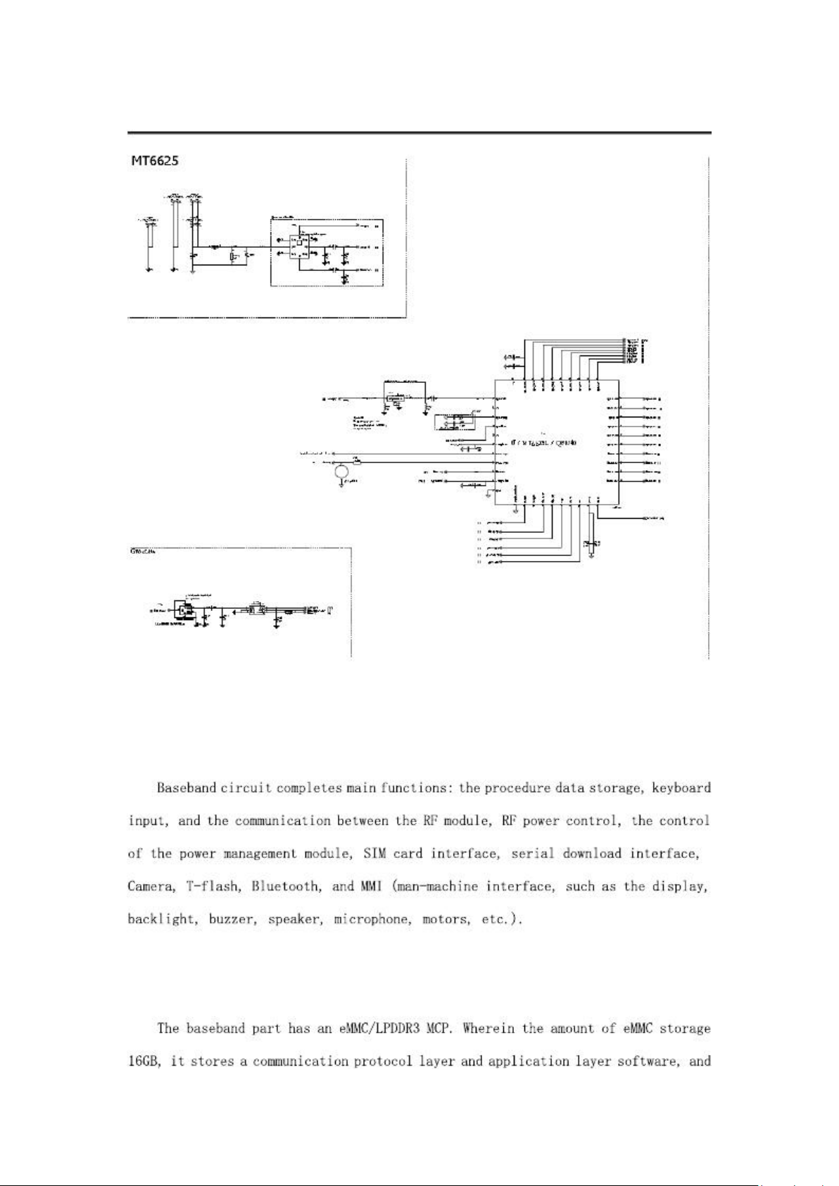
2.3 WiFi/BT/GPS Part
3. Baseband section
3.1 Outline
3.1.1 Memory
9
Page 10
3.1.2 Power Management
10
Page 11
3.1.3 Battery
Lithium ion polymer battery
3.1.4 32KHzCrystal
3.1.5 SIM Card
3.1.6 Audio frequency
11
Page 12
3.1.7 I/O Interface
3.1.8 Display
The main screen is 5.5-inch color screen 1776*1080 FHD
Before cutting board after the completion of the production line SMT X-RAY inspection,
according to the actual situation, X-RAY examination can not be found 100% badness, X-RAY
inspection may omissions some fault plate flow down. If found fault plate in the testing process,
the first step is to re-check of the X-RAY and carefully to see if there is even welding, lap welding,
Weld, if normal, analyze the situation following the positioning
3.2.1 Power failure Check
The failure phenomenon caused by a power failure: can not boot, shutdown leakage current
boot large current.
The main reason for the problem: Weld, electrical the original filtering or ESD device to
short-circuit, burning with the device is connected to a power source.
Positioning as well as steps to solve this type of problem is as follows
1 Troubleshoot and connected to the power supply components of the welding, Weld, or the
peripheral devices even tin
2 with a multimeter rule out whether there is power to short-circuit, and step by step to
troubleshoot the cause of the short (mainly: even tin, IC burned ESD protection device
breakdown, capacitor breakdown)
3 boot to test the power output is normal
If a power output value is not normal, whether the view filter capacitor welding problems,
whether the breakdown, filter capacitor is broken, replace; excluded one by one, and finally you
can navigate to the main chip damage
Each the power test position and the normal boot value is shown in the following table
12
Page 13
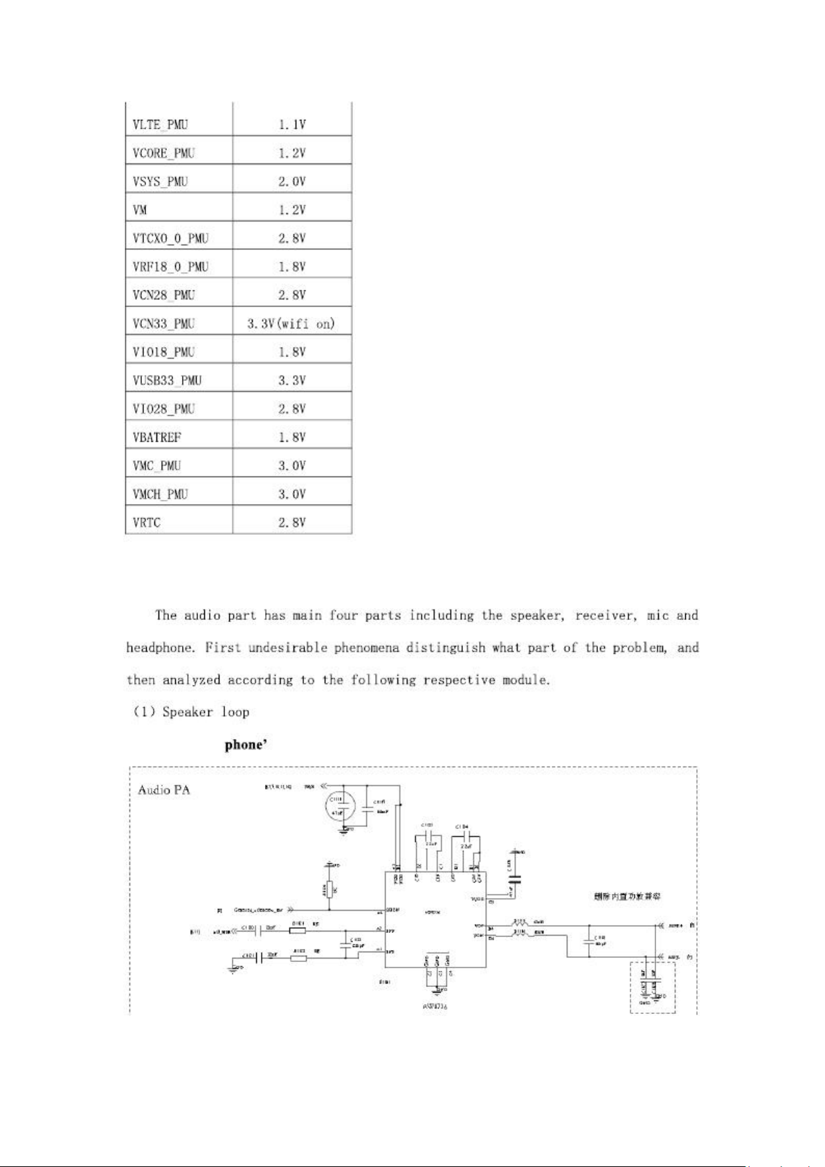
3.2.2 Audio faults
The FS554-
s speaker circuit is as follow
13
Page 14

Speaker Loop
Speaker Common faults and reasons
1 SPK Ringtones reasons: 1) light board,audio PA bad, SPK itself is bad, or the
connection FPC problem, the whole observation board board PFC Cartridge is
skew, not in place 2) relevant component there is dry welding 3 ) software
problems
2: SPK ringtones or murmur: 1) software volume settings 2) SPK ontology reasons
3. Switch machine ringtones, but engineering tests SPK OK: 1) scene mode is set to switch
machine ringer off 2) software problems, itself boot ringtones;
(2) Receiver circuit
FS554- phone receiver is embedded in the mobile phone front shell through shrapnel and
motherboard connection. Mainly used for the call. Receiver circuit diagram as shown below.
Receive Loop
14
Page 15

Main MIC
4 Headphone loop
FS554- phone use headphones with a 3.5mm headphone. Its circuit diagram is as follows:
Headphones common faults and reasons:
1, headphones only one channel sound: 1) the headset is not inserted in place 2) Relevant
component Weld. 3) Relevant component breakdown shorted to ground;
2 headphone left and right channels are no sound: 1) the headset is not inserted in place 2)
Relevant component breakdown on the short circuit;
3, unplug the headphones bank borrowing does not recognize: 1) Relevant component Weld;
2) whether headphones Block shrapnel and motherboard good contact 3) software reasons
4 headset MIC no transmitter: 1) the headset is not inserted in place 2) Relevant component
Weld 3) Relevant component breakdown on short-circuit;
15
Page 16

3.2.4 LCD Fault
The part of the circuit schematic as shown below. Common problems and causes of the LCD
module
16
Page 17

17
Page 18

3.2.5 FM
The CPU controls FM IC working condition through the I2C signal, when FM is
working, should insert headphone as its antenna. FM outputs audio signal to the CPU
Codec, amplify playing or record. FM common faults and causes:
1, FM cannot search frequency or less frequency reason: 1) headphone without
inserting or not insert good 2) surrounding environment is bad, such as plant, garage, etc.
FM signals itself is weak or no FM signals source 3) FM antenna circuit exists poor
soldering or short circuit, lead to unable to receive FM signals or FM signals leak 4)
software reason
2 FM without sound reasons or murmur 1) this FM radio frequency is invalid 2) FM
weak signal 3 related component bad-welding 4) headphone was not put in place; 5)
whether headphone socket shrapnel contacts with the mainboard well 6) whether headphone
socket welding is OK
3 FM module operation failed. 1 Check whether the I2C and CLK signal are normal
or not 2 Software fault
18
Page 19

3.2.5 Bluetooth
FS554-
BT adopts MT6625LN/A chip. Data transfer interface and audio interface are
directly connected to the CPU. Common failures are:
1, Bluetooth function failure, you need to check the Bluetooth is turned on, the
Bluetooth Visibility settings are correct. The Bluetooth power supply and clock circuit
the existence of the phenomenon of short circuit or Weld.
2, Bluetooth effective distance is short, easily disconnected. Need to check
whether Bluetooth antenna circuit soldered or short circuit, Bluetooth antenna and
motherboard contact well.
3.2.6
WIFI
fault
WIFI function failure, you need to check the WIFI is turned on, WIFI visibility settings are
correct. WIFI power supply and clock circuit whether there is a short circuit or Weld phenomenon.
19
Page 20

3.2.6 Camera fault
Connect with the CPU through a dedicated Camera IF port. Camera control is done through
the I2C bus. Camera common fault and why:
1, Camera initialization failed, could not enter the Camera the main interface. 1) Camera poor
welding or poor contact 2) the Camera Ontology failure 3) Camera Power supply is not normal
(Weld, or short-circuit led to) 4) related components welding problems
2, Camera Preview shows blurred screen or color is not normal. 1) Camera poor welding or
poor contact. 2) related components welding 3) restore the factory settings after restart
3, Camera other problems, please replace the Camera try to confirm whether the Camera
body has problems.
20
Page 21

3.2.7
SIM card failure
FS554- SIM card module circuit is connected directly with PMIC through eight-path signal from
SUIM slot. The major failure of the module does not know the card, the reason usually: 1) USIM
21
Page 22

card GSM card and USIM deck poor contact 2) poor USIM card socket welding 3) software
problem cause the phone to pick a card, change the card to confirm. 4) SIM card holder exist Weld;
5) card exceeds the itinerary or inserted upside.
3.2.8 Motor test is invalid
FS554- adopts flat motor, with simple circuit. As shown below. Common motor failures and
the reasons are:
1, the motor without vibration 1) motor and motherboard contacted poor 2) motor body bad 3)
C907, L901 bad 4) whether the FPC installed partial
2, the motor was felt as weak 1) motor ontology bad) the cause of the software settings
3 motor vibration sometimes 1) motor and motherboard poor contact
22
Page 23

3.2.9 Gravity Sensor
FS554 G-Sensor circuit is very simple, Power offer power to the Sensor IC power, I2C bus
transfer command and data. G-Sensor faults and the reasons:
1, Sensor without functions: whether the paster is OK
23
Page 24

3.2.10 T-Flash fault
FS554 T - Flash circuit is connected with CPU through the special SDIO bus, circuit
diagram shown below. T - Flash the common faults and reasons are:
1, T Flash read-write test is failure. 1) T - flash for fault card or and T kaka seat have had no
contact with good 2) below the resistance there may be short circuit, or virtual welding
phenomenon. Capacitance may on short circuit. (using a multimeter to test whether T card signal
and ground and VMCH short circuit can eliminate) 3) software reason
2, T card not to know card: T holder PIN feet virtual welding, on MLV welding reverse and
capacitance breakdown
3, T - Flash can't through the USB for transmission. 1) T - Flash itself, speaking, reading and
writing test failure fault 2) software fault 3) USB fault
24
Page 25

T card circuit
3.2.11Touch Panel function
Touch Panel common fault and reasons are:
1. The Sensor sensitivity low, slow reaction: software problem;
4. Touch Panel function NG, at present is mainly due to FPC itself partial long cause, the I2C
initialization failed;
TP circuit
25
Page 26

3.2.13 Cannot boot failure
Can't boot failure is the phone fault with highest probability of occurrence. Software
problems, welding problem, device failure is the main factor causing failing to boot. Maintenance
process can cooperate with LCD and startup current, as well as the keyboard and so on to orientate
approximately.
1, Power off leak current is large. The main failure reason is VBAT connected components
had to earth short circuit problem. Usually radio frequency PA burned or welding problem cause.
The simpler method is looking for is a hot devices, general such devices have larger may on short
circuit.
2, Boot without current, LCD no display, keyboard, etc not bright. 1) boot key SMT bad 2)
battery connector bad contact (through the plug charging machines)
3, Crashed when boot, 1 can try to re-download the software, 2 replace memory
4, Current is large when boot. LCD displays normally, even can enter the IDIE interface,
single board is very hot 1) The individual power circuit short circuit to ground phenomenon exists
in the phone, which is usually the problem that ESD protective devices of module circuit
breakdown short circuit to ground or weld problems.
26
Page 27

27
Page 28

30
Page 29

31
Page 30

32
Page 31

33
Page 32

34
Page 33

35
Page 34

36
Page 35

37
Page 36

38
Page 37

39
Page 38

40
Page 39

~4.1V .
41
Page 40

Page 41

Page 42

42
 Loading...