

Fly FS514 Service Manual

Maintenance Manual
1
Service Manual

Maintenance Manual
2
Contents
1. OUTLINE ............................................................................................................... 3
1.1.Mobile Introduction ........................................................................................................................................ 3
1.2.Motherboard Components Distribution ....................................................................................................... 4
1. SIGNAL FLOW AND FAULT ANALYSIS ............................................................. 5
2.1. RF Part ............................................................................................................................................................ 5
2.1.1. Block Diagram of the RF Section ............................................................................................................. 5
2.1.2. Signal flow of the RF Transmitting Part ................................................................................................... 6
2.1.2.1. Transmitting Path ............................................................................................................................. 7
2.1.3. Signal Flow of the RF Receiving Part ....................................................................................................... 7
2.1.3.1. Receiving Path Components ............................. .............................................................................. 7
2.2. Baseband part ................................................................................................................................................. 9
2.2.1 Block diagram of the Baseband part........................................................................................................... 9
2.2.2 Power Management .................................................................................................................................... 9
2.2.3 Audio Section ........................................................................................................................................... 12
2.2.3.1 Audio Codec Circuit ........................................................................................................................ 12
2.2.3.2 MIC& Receiver Loop ...................................................................................................................... 12
2.2.3.3 Headset Loop ................................................................................................................................... 13
2.2.4 Baseband Fault issues ............................................................................................................................... 14
2.2.4.1 Analysis of the keyboard fault ........................................................................................................ 15
2.2.4.2 Analysis of Display module circuit ................................................................................................. 15
2.2.4.3 FM Module ...................................................................................................................................... 17
2.2.4.4 Camera Module ............................................................................................................................... 17
2.2.4.5 IO Interface ..................................................................................................................................... 19
2.2.4.6 SIM Card Circuit ............................................................................................................................. 19
2.2.4.7 Memory Card Circuit ...................................................................................................................... 21
2.2.4.8 BT/WIFI/GPS Circuit...................................................................................................................... 21
2.2.4.9 G-sensor Circuit .............................................................................................................................. 22
2.2.4.10 ALS/P-sensor Circuit .................................................................................................................... 22
2.2.4.11 Hall Circuit………………………………………………………………………....…………….22
Maintenance Manual
3
Product Hardware Definition
Base Chip Set
BB
MT6580A/WA
PMIC
MT6350V/A
Transceiver
MT6580A/WA
Camera DSP/MMD
NA
RF PA
HS8684
FM
MT6580A/WA
BT
MT6580A/WA
Audio CODEC&PA
AW8736FCR
Memory
Kingston 08EMCP08-EL3CV100-C50
TP IC
GT615
Peripheral
Configuration
LCD
ILI9881
Backlight driver
ET5120A
Memory Card
UP 32GB
Antenna
Basic
Performance
Indicators
Leakage current
≤200uA
Standby current
≤7mA
Call current as
maximum power
470mA
Board-level
power
GSM
32.5dBm
DCS
29.5dBm
Board-level
receiver
sensitivity
GSM
-108.5dBm
DCS
-108.5dBm
TRP
GSM
28.5dBm
DCS
26.5dBm
BAND1
18dBm
BAND8
19dBm
TIS
GSM
-103.3dBm
DCS
-104.4dBm
BAND1
-104.2dBm
BAND8
-104.1dBm
1. Outline
1.1. Mobile Introduction

Maintenance Manual
4
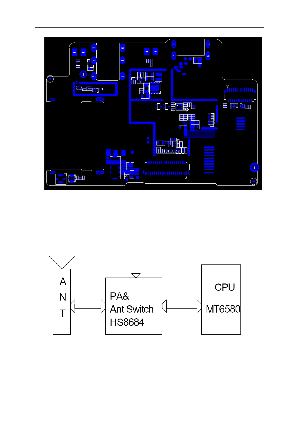
1.2. Motherboard Components Distribution
Maintenance Manual
5
2. Signal Flow and Fault Analysis
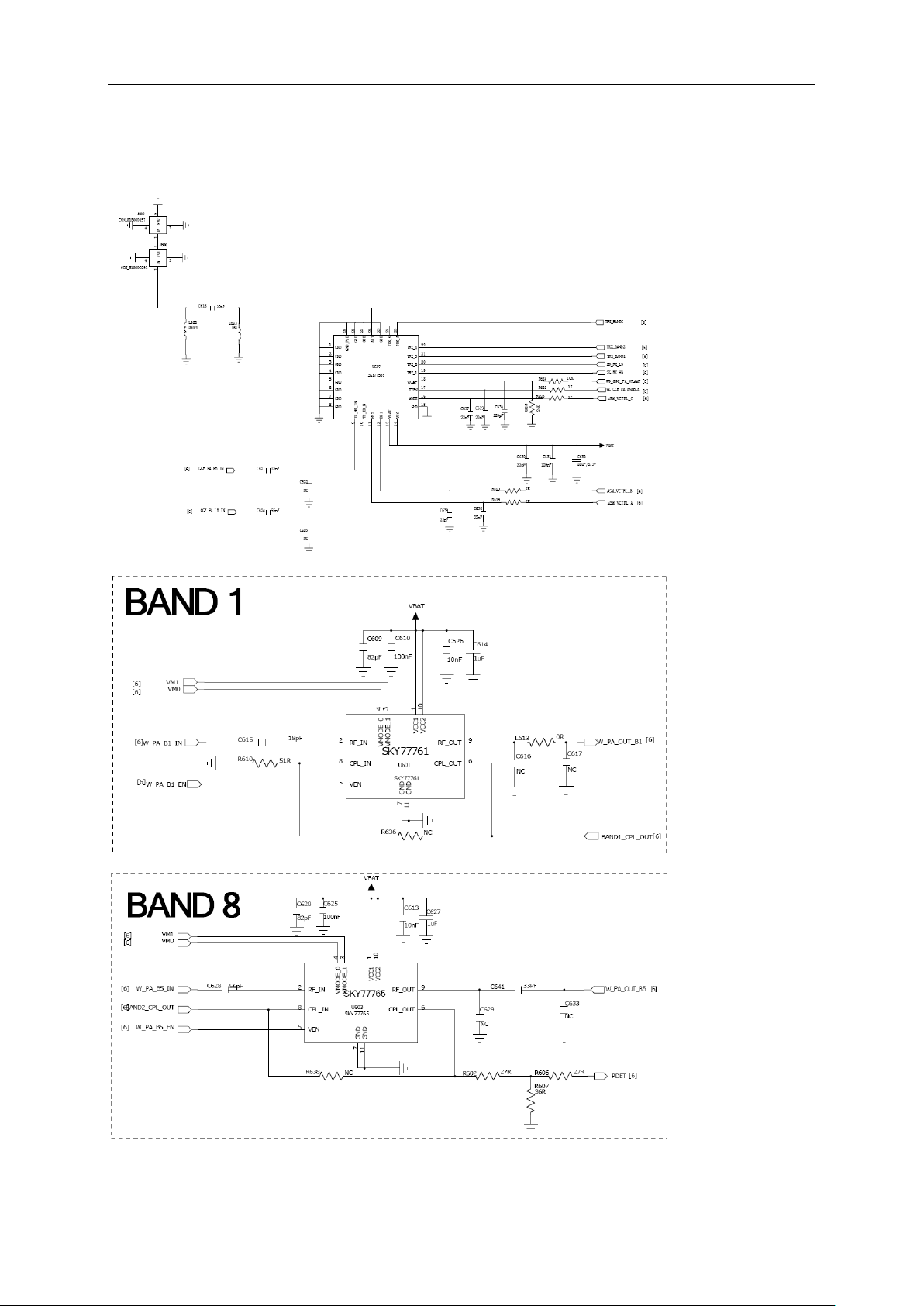
2.1. RF Part
2.1.1. Block Diagram of the RF Section
RF Block Diagram
Maintenance Manual
6
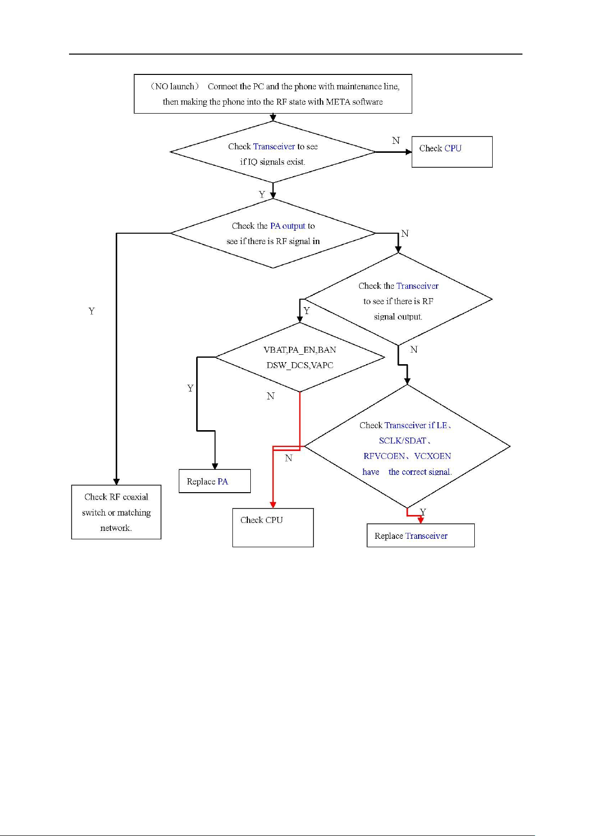
2.1.2. Signal flow of the RF Transmitting Part
2.1.2.1. Transmitting Path
Maintenance Flow Chart of the Transmitting Issue:
Maintenance Manual
7
2.1.2. Signal Flow of the RF Receiving Part
2.1.3.1. Receiving Path Components
Receiving path is shown in the following figure:
 Loading...