


FLY SERVICE SUPPORT
1
FS509 Nimbus 9
Service Manual

FLY SERVICE SUPPORT
2
Contents
1. Outline ................................................................................................................................3
1.1. Mobile Introduction ............................................................................................3
1.2. Motherboard Components Distribution .............................................................5
2. Signal Flow and Fault Analysis ............................................................................................6
2.1. RF Part .................................................................................................................6
2.1.1. Block Diagram of the RF Section..........................................................................6
2.1.2. Signal flow of the RF Transmitting Part ...............................................................6
2.1.2.1. Transmitting Path .......................................................................................6
2.1.3. Signal Flow of the RF Receiving Part....................................................................8
2.1.3.1. Receiving Path Components ......................................................................8
2.2. Baseband part ................................................................................................... 10
2.2.1. Block diagram of the Baseband part ................................................................ 10
2.2.2. Power Management ......................................................................................... 10
2.2.2.1. Mobile power supply system .................................................................. 10
2.2.3. Audio Section .................................................................................................... 13
2.2.3.1. Audio Codec Circuit ................................................................................ 13
2.2.3.2. MIC& Receiver Loop ............................................................................... 13
2.2.3.3. Headset Loop .......................................................................................... 14
2.2.4. Baseband Fault issues ....................................................................................... 15
2.2.4.1. Analysis of the keyboard fault ................................................................ 15
2.2.4.2. Analysis of Display module circuit .......................................................... 16
2.2.4.3. FM Module ............................................................................................. 16
2.2.4.4. Camera Module ...................................................................................... 17
2.2.4.5. IO Interface ............................................................................................. 18
2.2.4.6. SIM and T_Flash Card Circuit .................................................................. 19
2.2.4.7. BT/WIFI/GPS Circuit ................................................................................ 20
2.2.4.8. G-sensor Circuit ...................................................................................... 20
FLY SERVICE SUPPORT
3
1. Outline
1.1. Mobile Introduction
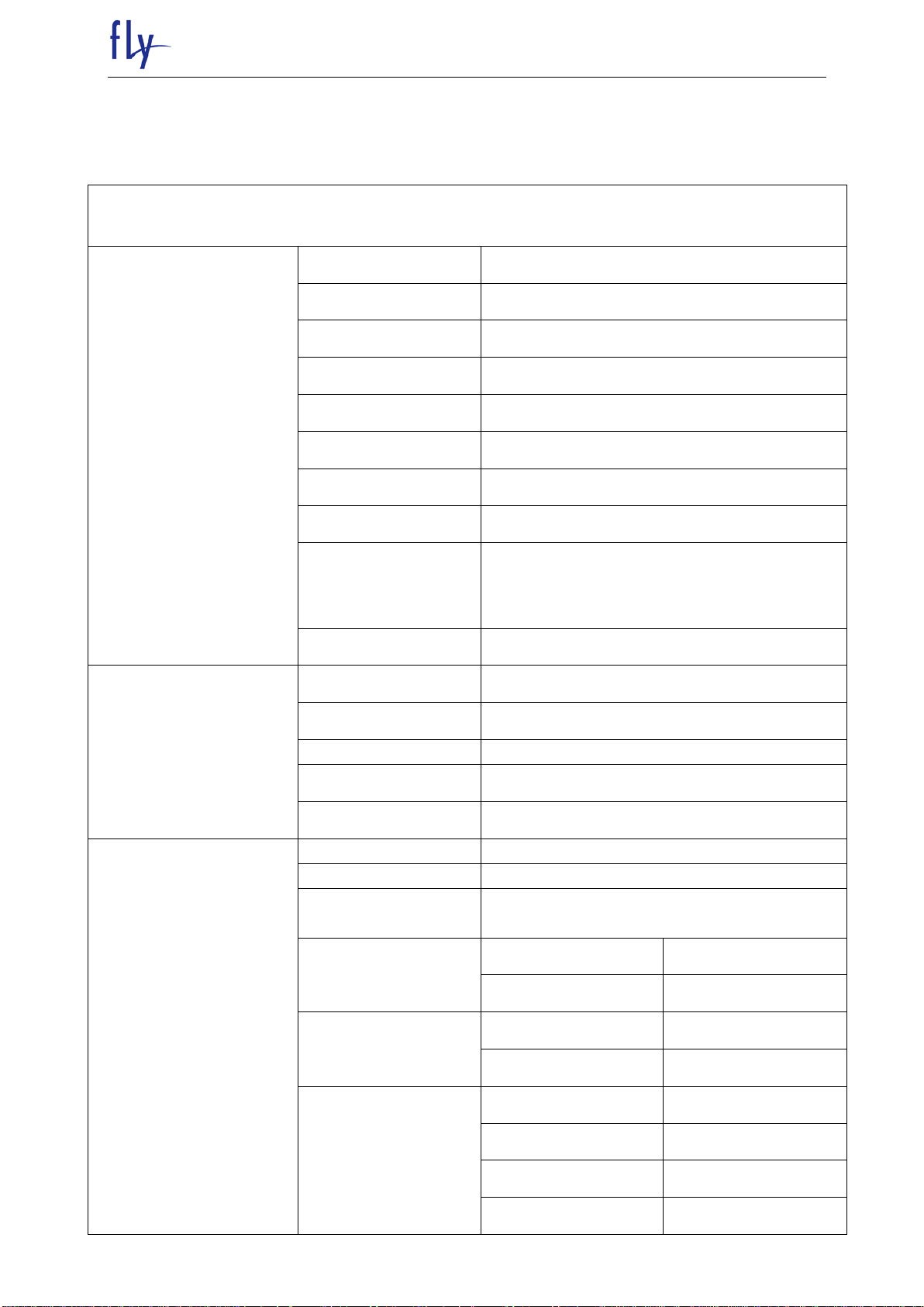
Product Hardware Definition
Base Chip Set
BB
SC7731C
PMIC
SC7731C
Transceiver
SR3533G
Camera DSP/MMP
NA
RFPA
VC7590-21; VC5318
FM
SR2351C
BT
SR2351C
Audio CODEC&PA
SC7731C
Memory
MT29TZZZ8D5BKFAH-125 W.95K,MICRON
08EMCP08-EL3CV100-C50,KINGSTON
TYD0GH121661RA,TOSHIBA
TP IC
NA
Peripheral Configuration
LCD
Backlight driver
DIO5661TST6
CAMERA
5million pixel
Memory card
NA
Antenna
Basic Performance Indicators
Leakage current
≤ 90uA
Standby current
≤ 7mA
Call current as maximum
power
TBD
Board-level power
GSM
32 dB
DCS
29 dB
Board-level receiver
sensitivity
GSM
-108 dB
DCS
-108 dB
TRP
GSM
28 dB
DCS
26 dB
Band1
18 dB
Band8
18 dB
FLY SERVICE SUPPORT
4
TIS
GSM
-103 dB
DCS
-103 dB
Band1
-103 dB
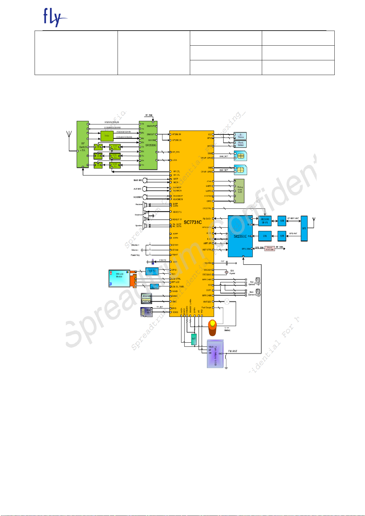
System Block Diagram
FLY SERVICE SUPPORT
5
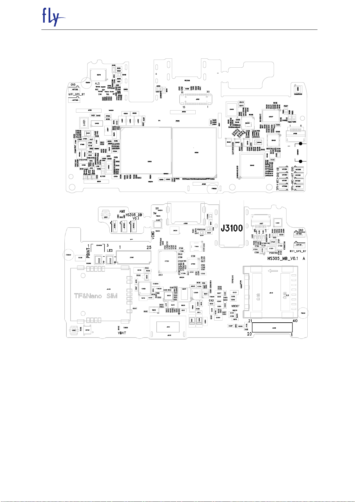
1.2. Motherboard Components Distribution
FLY SERVICE SUPPORT
6
2. Signal Flow and Fault Analysis
2.1. RF Part
2.1.1. Block Diagram of the RF Section
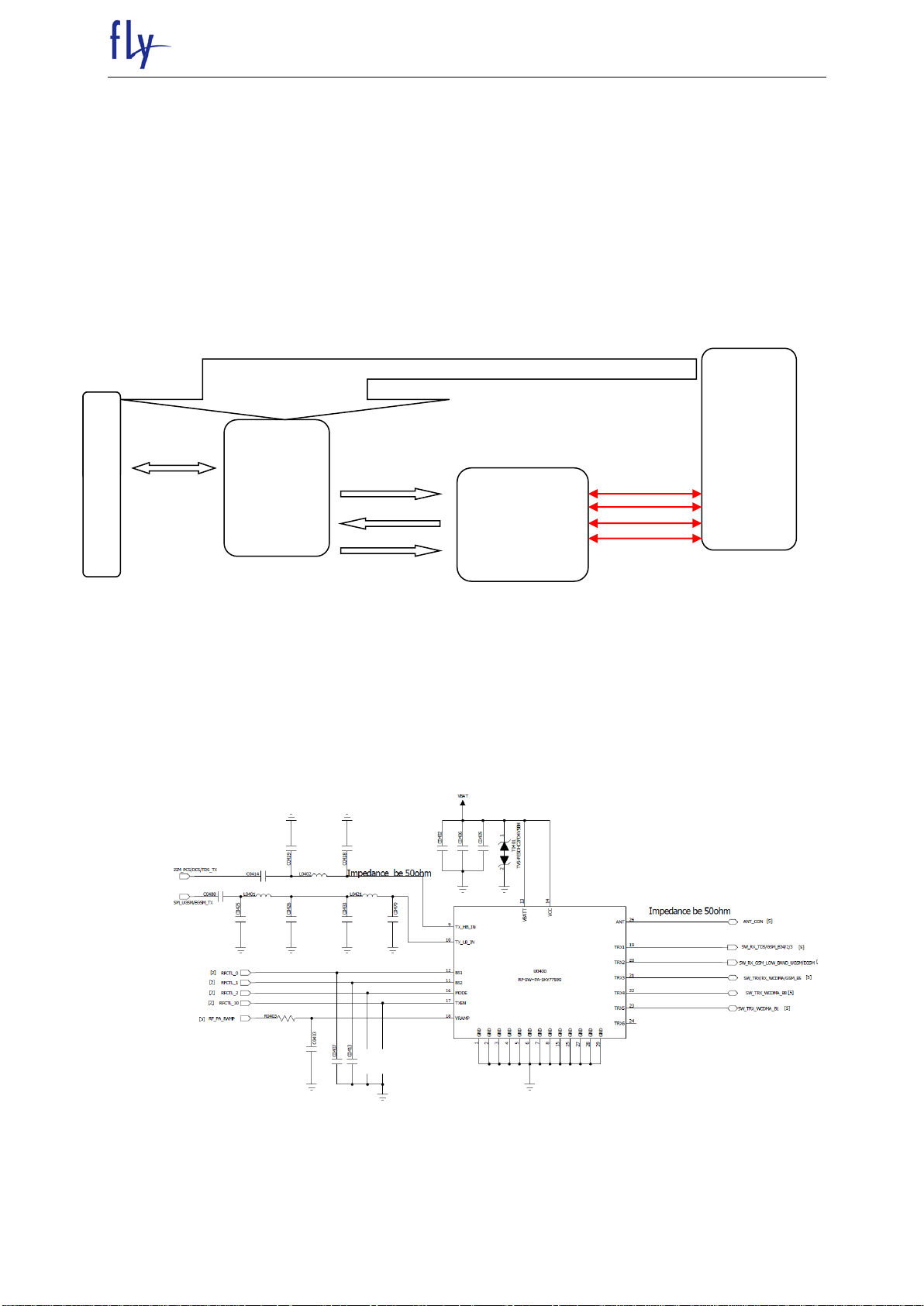
RF Block Diagram
2.1.2. Signal flow of the RF Transmitting Part
2.1.2.1. Transmitting Path
A
N
T
A
N
T
PA &
Ant Switch
VC7590-21
Transceiver
SR3533G
CPU
SC7731C
 Loading...