


FLY SERVICE SUPPORT
1
FS452 Service Manual V1.0

FLY SERVICE SUPPORT
2
Contents
1. FS452 overview ............................................................................................................... 3
1.1 FS452 brief introduction ......................................................................................... 3
1.2 Function diagram .................................................................................................... 4
1.3 Mainboard component distribution diagram ........................................................... 5
1.4 Main IC Names ....................................................................................................... 6
2. RF .................................................................................................................................... 7
2.1 RF Overview ........................................................................................................... 7
2.2 RF circuit description .............................................................................................. 8
2.3 WiFi/BT/GPS /FMPart .......................................................................................... 11
3. Baseband section .......................................................................................................... 12
3.1 Outline .................................................................................................................. 12
3.2 Common Failure Analysis and Maintenance ........................................................ 13
3.2.1 Power failure Check ................................................................................... 13
3.2.2 Audio faults ................................................................................................. 14
3.2.3 LCD Fault ................................................................................................... 19
3.2.4 Camera fault ............................................................................................... 18
3.2.5 SIM card failure .......................................................................................... 19
3.2.6 Motor test is invalid .................................................................................... 19
3.2.7 Gravity Sensor ........................................................................................... 20
3.2.8 T-Flash fault ................................................................................................ 20
3.2.9Touch Panel function ................................................................................... 21
3.2.10 ALS&PS
Sensor.................................................................................................25
3.2.11 Cannot boot failure ................................................................................... 21

FLY SERVICE SUPPORT
3
1. FS452 overview
1.1 FS452 brief introduction
The development and design of the FS452 PCBA is based on SC7731 platform. The
mainboard system mainly consists of the chip SC7731+SR3131+SR2351C, which are
responsible for three part functions, namely, baseband, radio frequency and power
management chip. FS452 PCBA is an all-in-one phone mainboard, which supports GSM,
WCDMA, and covers Bluetooth, WIFI, Camera, FM functions, and so forth.
The maintenance of mainboard is one of the important links among mobile products
rear-end producing. The speed and quality of maintenance relate to the rate of good products,
production efficiency, and cost control throughout the producing. In the case of a reasonable
design of product, in the end-producing, finding the significant proportion in the bad board
should be SMT bad and component incoming material bad. So, when maintaining, first, start
with the two aspects. The principal means of fault diagnosis are: (1) find that bad welding spots
or components by microscopic examination and visual inspection; (2) guess failure positions
from the fault phenomena; (3) confirm the fault units by signal detection.

4
1.2 Function diagram
FLY SERVICE SUPPORT
FLY SERVICE SUPPORT
5
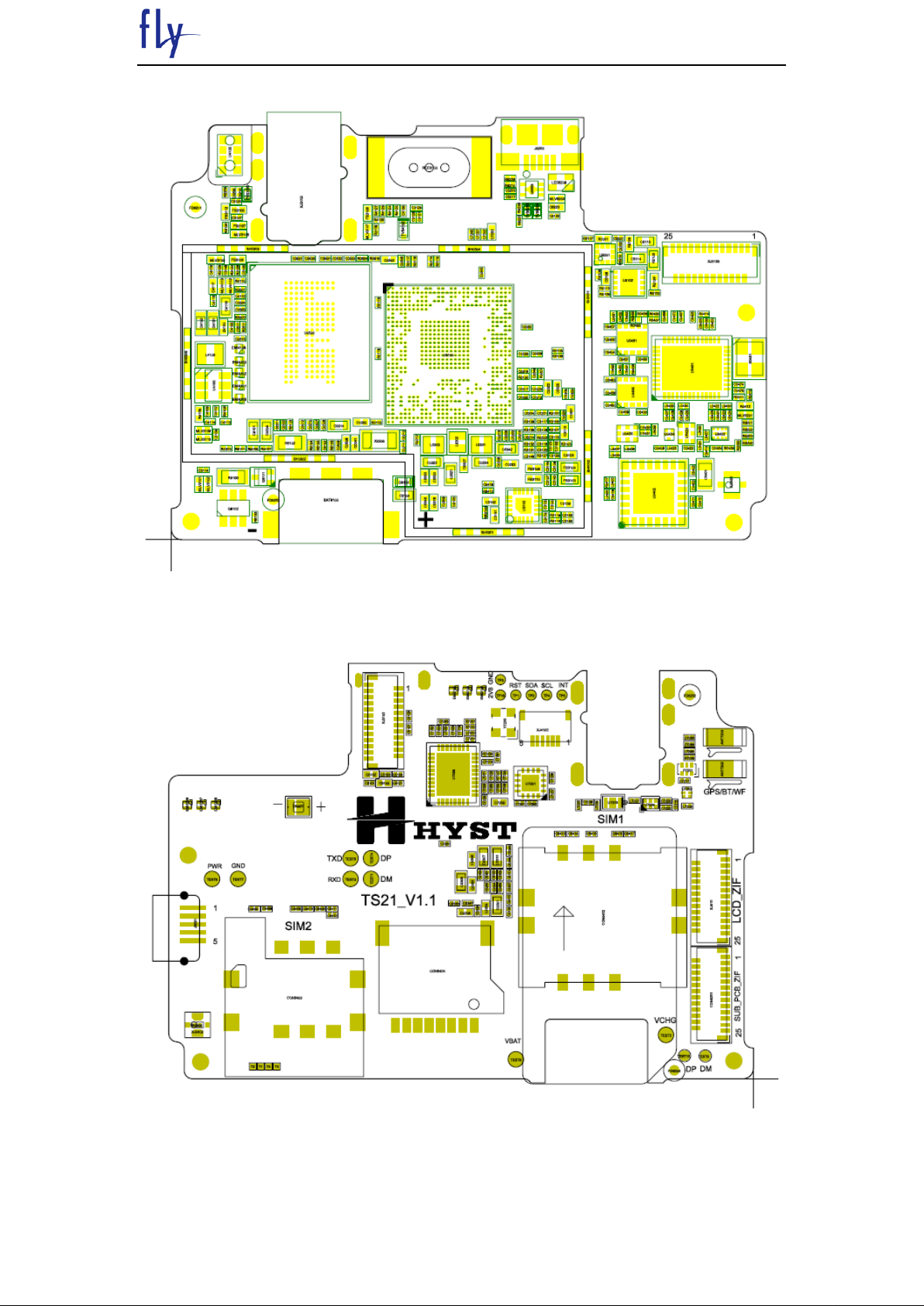
1.3 Mainboard component distribution diagram
Mainboard TOP
Mainboard BOTTOM
6
1.4 Main IC Names
order
attribute description
specifications
positio
n code
1
SC7731G;597;FCVFBGA;13.3X12.1;040;BB;WC
DMA
SC7731
U0100
2
SR3131;50;QFN; 5.5x7; 040; RF; 3G;RF
Transceiver
SR3131
U0401
3
SR2351C;38;QFN;5.5x4.5;040;RF;WIFI_BT_FM
_GPS Transceiver
SR2351C
U7206
4
eMMC+LPDDR2;1.8/3.3/1.2/1.8;4GB+4Gb;19ns/
533MHz;8/32;FBGA162,11.5x13,0x1.0mm,0.5m
m pitch
TYC0FH121638RA
U0500
5
RF SP4T TXM 4frequent
GSM/GPRS PA with 4 TRX ports,6x6x0.9mm
SC2662H
U0403
7
K class audio power amplifier
AW8733A
U3102
8
,2*2*1.1mm,1.7~3.6V,I2C/SPI
DA213
U5201
9
3in1 ALS&PS Sensor
AP3216
U4100
10
The flash drive
3mm×3mm TDFN-10 1A
EUP3611JIR1
U5102
11
radiofrequencyRFfilter 1in 4out double saw
GSM1800/1900 1.5×1.1×0.55mm
SFWG42KB002
U0422
12
BAND1 2016 WCDMA
SFXG50UZ502
U0423
13
The sound form frequency filter850M/1109
SFH881PA002
U0424
14
WCDMA Band8 2 x 1.6x 0.6mm 9pin
SFX897WZ102
U0425
15
3G PA;WCDMA band1 1920-1980M;3x3x0.9mm
10pin
SC2671H
U0451
16
3G PA;WCDMA band8 880-915M;3x3x0.9mm
10pin
SC2678H
U0455
17
SR2319A;16;QFN;2.5*2.5;050;RF
SAW+PA-2.4G
SR2319A
U7201
18
WIFI 2.450GHZ LCband-pass filter 2.0*1.2*0.9
SLFB21-2R450G-0
6TF
U7200
FLY SERVICE SUPPORT
FLY SERVICE SUPPORT
7
19
GPS 滤波器 1.1×0.9×0.5mm3
SFDG75BA002
U7202
20
LNA;GPS;XSON6,1x1.45x0.5mm
RDALN16
U7204
21
SAWfilterGPS-BT/WLAN DIPLEXER (demultiplex
er )
DP1608-V1524CA
T/LF
F7201
22
26M 2520 10PF ±0.5PPM(TCXO)(warm)
TXO952005-STO-3
218
Y7200
2. RF
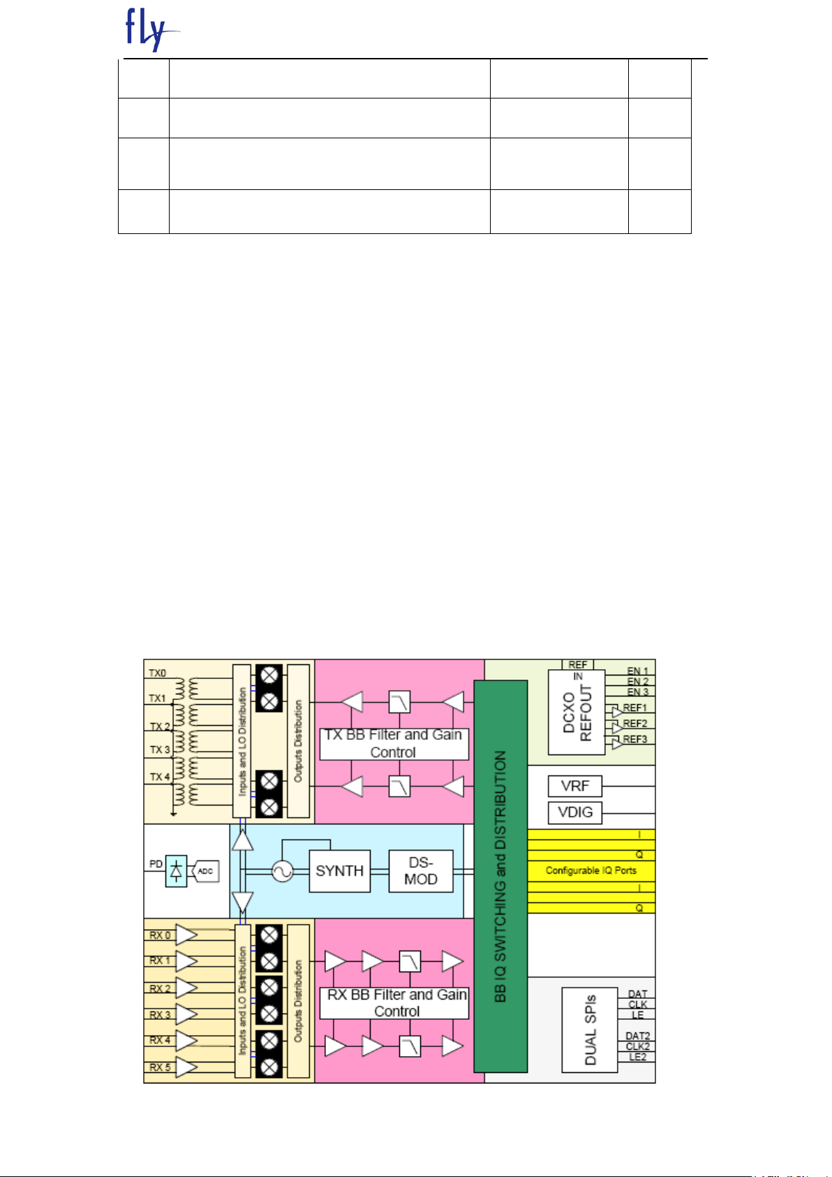
2.1 RF Overview
The SPREADTRUM SR3131 is a highly integrated RF cellular transceiver for
multimode (EDGE/GPRS/GSM/WCDMA/HSDPA/HSUP) and multiband (850/900/1800/
1900/2100MHz) applications. The device operates in any of the 3GPP bands i-x (with the
exception of band VII) and can be configured to interface with single-chain or multichain,
multimode power amplifiers (PAs). It supports HSDPA (cat. 1-14) and HSUPA (cat. 1-6)
and up to multislot class 33 EGPRS operation.
On the receive chain, the device integrates five high-performance low noise
amplifiers (LNAs) and uses a very low IF architecture ofr 2G and a highly linear direct
conversion receiver for 3G, eliminating the need for external LNAs and (WCDMA)
interstage RX SAW filters. The transmitter provides two low-noise high-band (1.7-2.1
GHz) and two low-noise low-band (800-900 MHz) multimode, multiband outputs that
eliminate the need for TX SAW filters in both modes of operation (2G and 3G).
Auto-calibration routines run internal to the transceiver, Providing robust performance
over the life of the part and simplifying factory calibration. The highly integrated device is
fabricated using a 21nm digital CMOS process and packaged in a 5.5 mm*7 mm FBGA.
RF framework block diagram
 Loading...