

Page 1

.
FLY EZZY5
SERVICE MANUAL
Page 2

CONTEANT LIST
Chapter 1: Summary
Chapter 2: Exploding Diagram
Chapter 3: Explanation of Schematic
Chapter 4: Failure Analysis
Chapter 5: Manual of tool software
Chapter 6: Tools List
Page 3
Chapter 1: Summary
Standby time: 150~200 hours
Talking time: 300~450 mins
Style of network
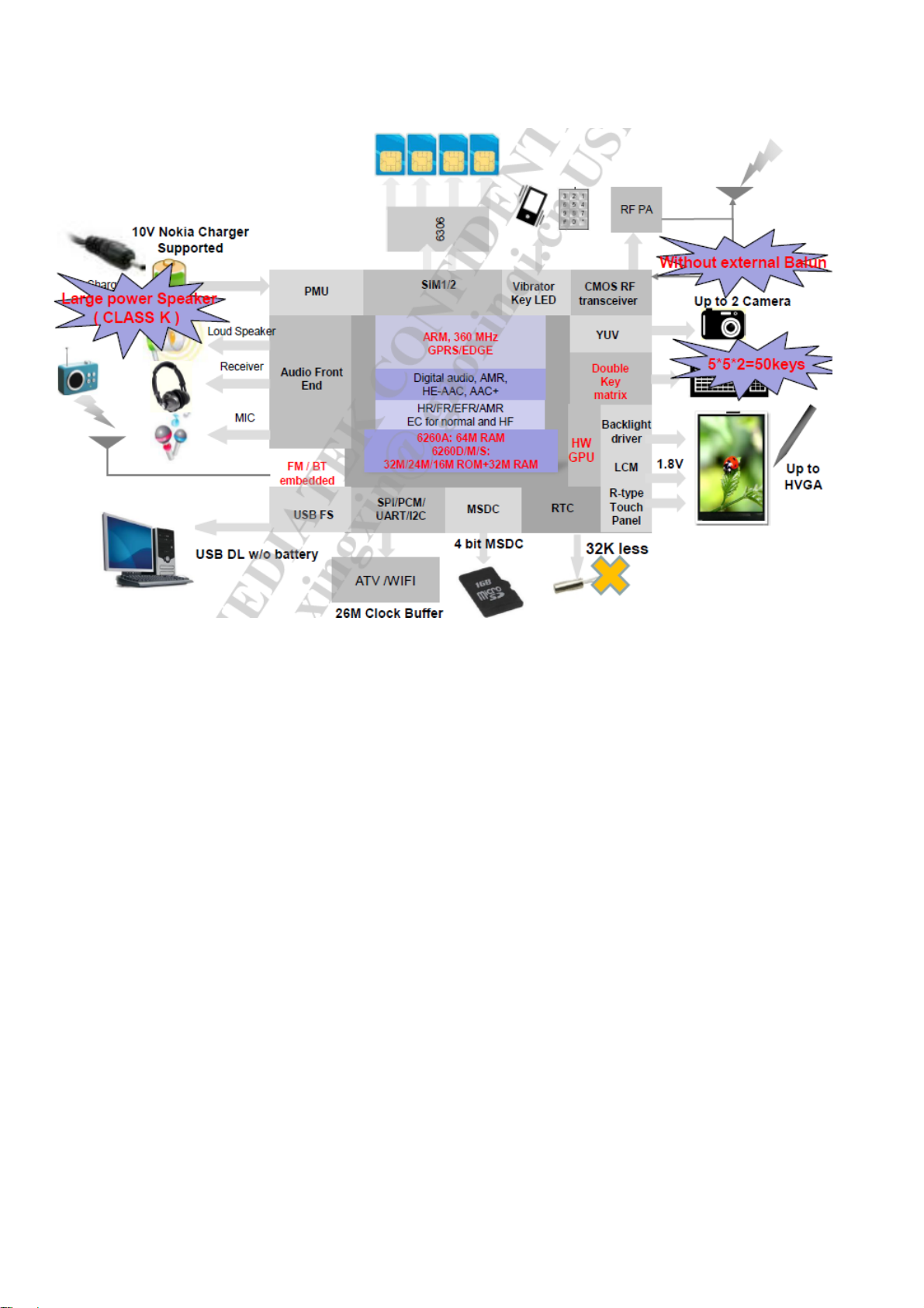
GSM900, DCS1800
This streamline and comfortable handset is a perfect combination of humanized design and
Excellent craft. Besides the basic call function, FLY Ezzy5 provides you with a collection of
practical Functions including sweet ring tone, cartoon incoming-call animation, File manager
(T-Flash card support). It also supports MMS and increment service which facilitate your
work and entertainment.
In order to support technicians to be familiar with FLY Ezzy5 handset, please master the method of
servicing. In addition, we provide corresponding technical data, including CKT base band, RF and
software. There are also many base band and RF test reference points and description of circuit.
You can refer to maintaining examples. Hope it could give you some help.
Main specification and technique standards of FLY Ezzy5 are as below:
Page 4
Chapter 2: Exploding Diagram
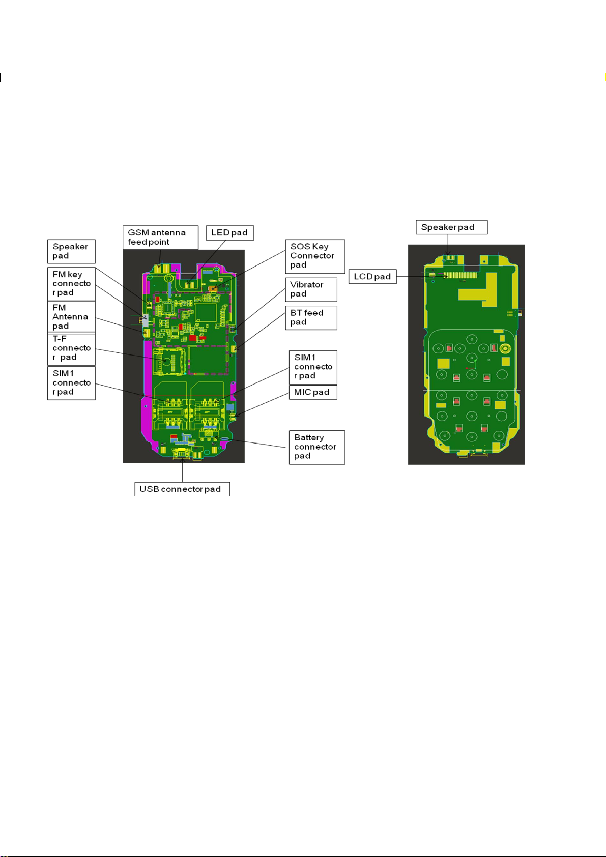
Page 5
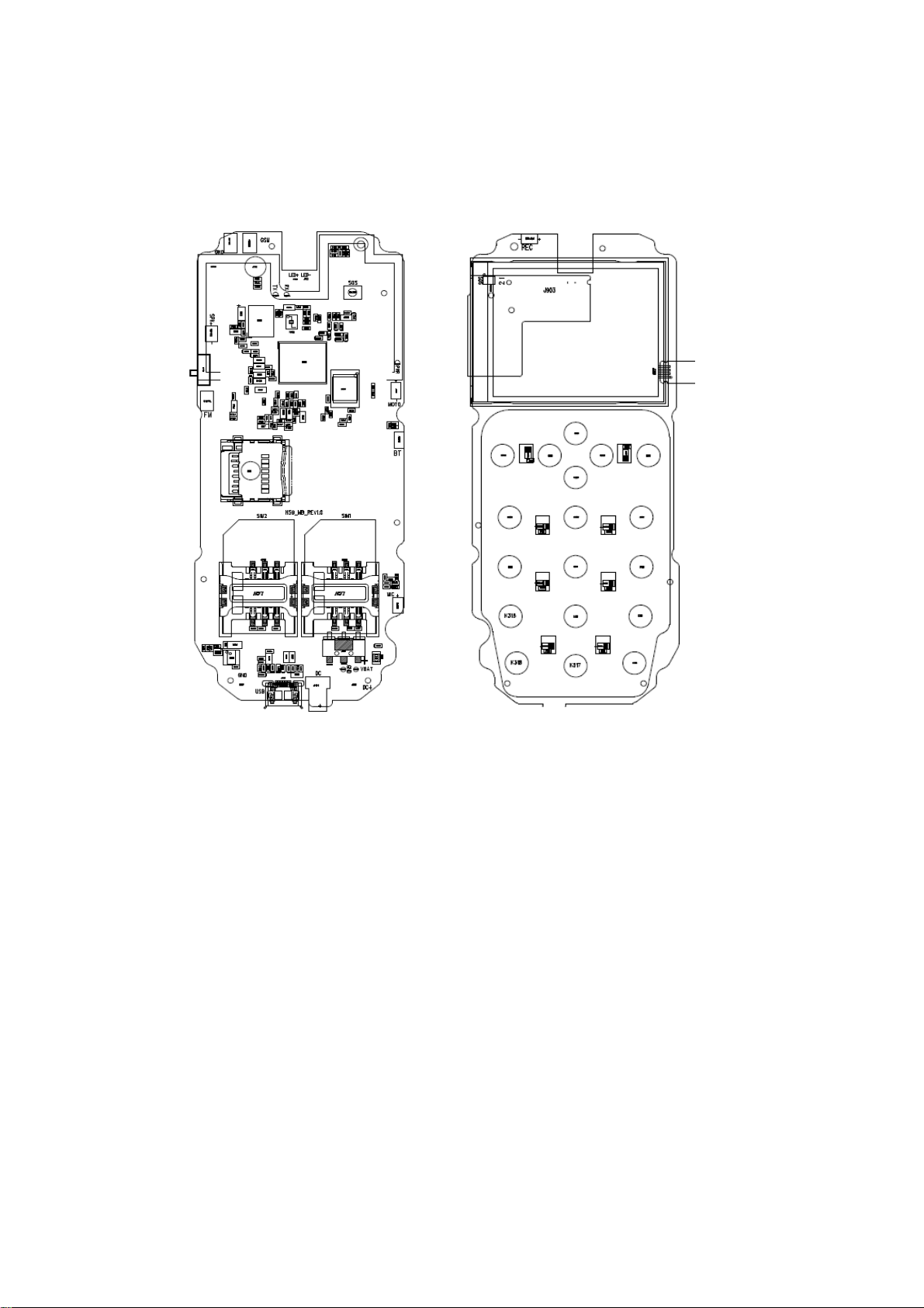
The main board placement
Page 6
Chapter 3: Explanation of Schematic
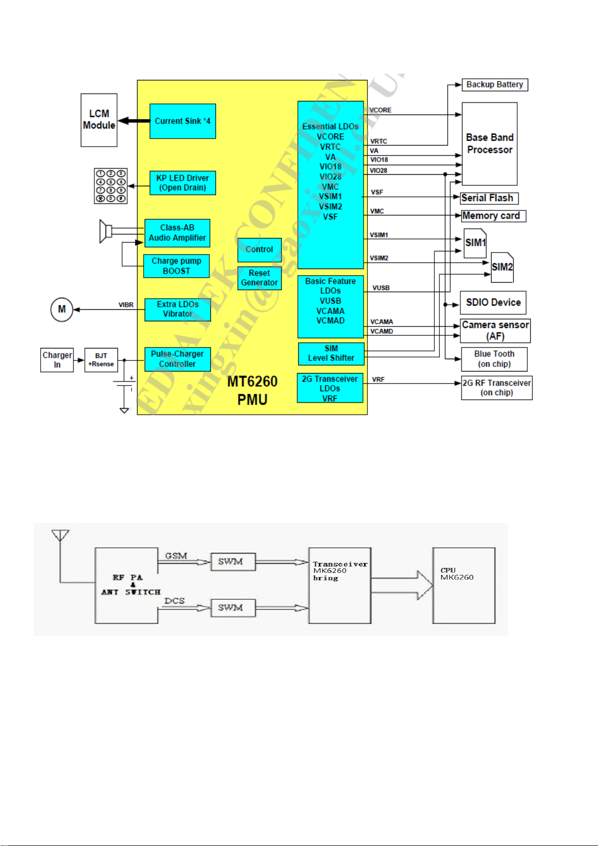
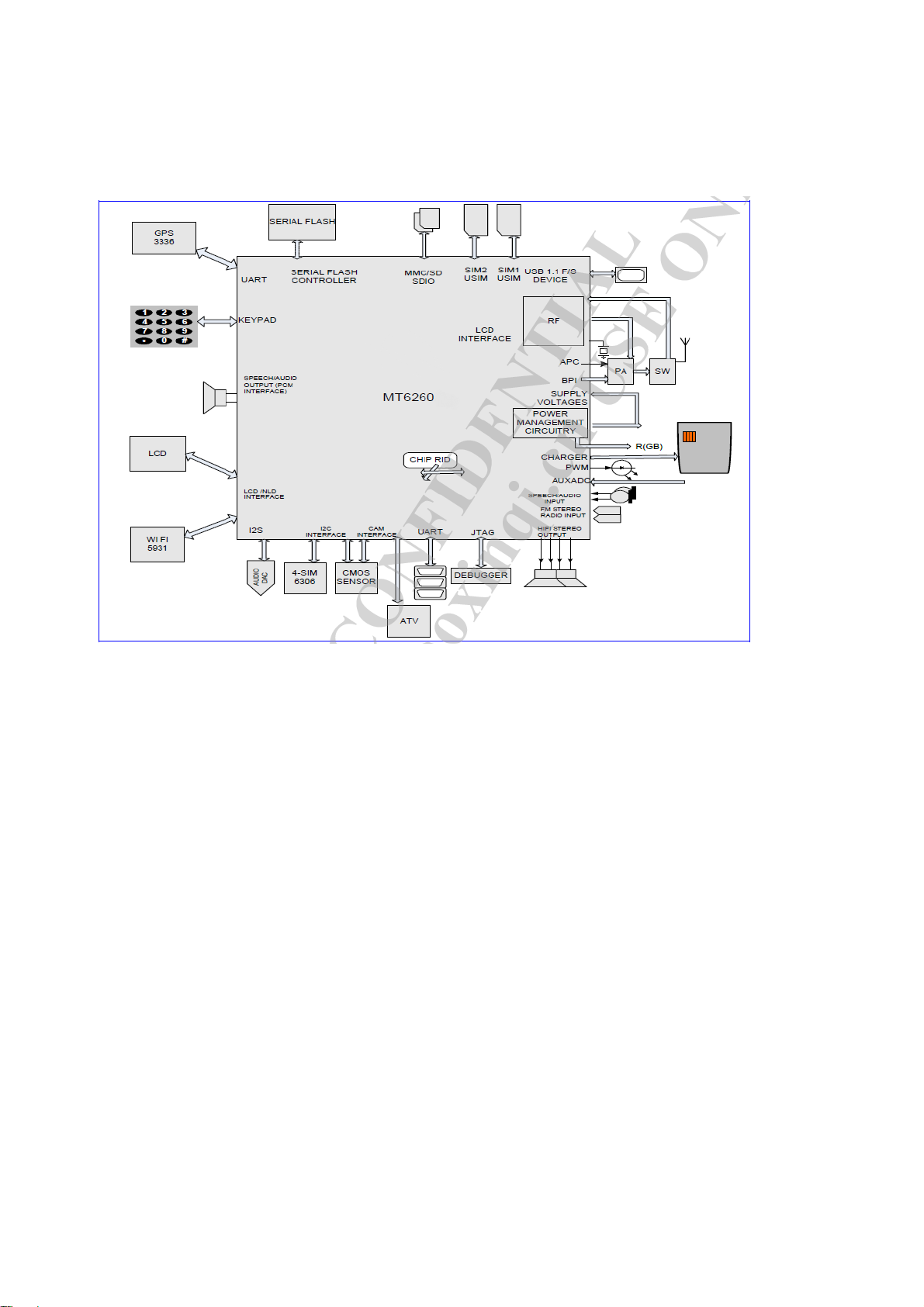
Picture 3.1 MT6260 principle picture
3.1 Principle of RF circuit
3.1.1 Principle of receiver circuit
3.1.1.1Rx signal flow chart:
Picture 3.1.1 Receive signal flow frame
Page 7

3.1.1.2 Main function of RF
RF part generally means the analog RF and IF process system ,including Antenna system、 TX
path、RX path、Analog modem and Frequency Synthesizer .
RF Circuit deals with the RX and TX of wireless signal, with responsibility for the bidirectional
Transmission of speech and data between the MS and BS through the air interface. In detail RX part
Accomplishes the AGC amplifying, mix and demodulation of RF weak signal received from BS, The Final
signal output from RX part is the analog baseband I/Q signal. The final RX I/Q will be sent to Baseband
Circuit for later disposal. On the other hand TX part deals with the signal modulation, Up-conversion mix
and power amplifying of analog I/Q signal received from baseband, generating Burst which meets the GSM
specification. And then the bursts are transmitted to Base station through The antenna. The signal
interface between RF Circuit and Baseband is analog baseband I/Q signal. The Performance of RF Circuit
can directly affects the signal transmission quality of the mobile phone!
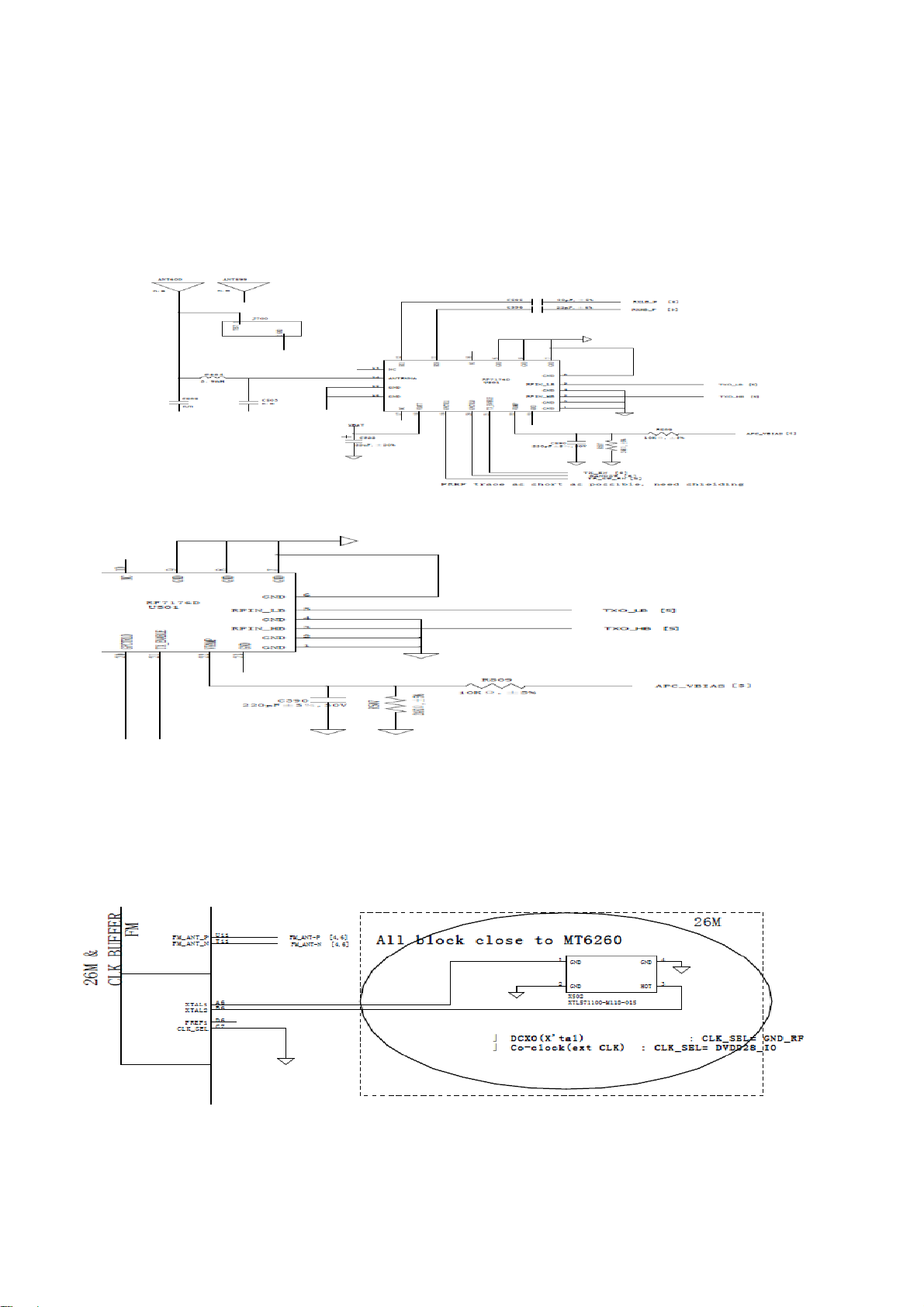
The schematic of RF block for MTK GSM Dual-band RF solution is show below:
From the chart we can see that the RF part is mainly composed of a highly integrated CMOS
Transceiver chip (MT6260), some RX Saw filters, reference crystal oscillator, power amplifier,
Antenna switch module, antenna and the matching components between each other...
3.1.2 Direct Conversion Receiver
-Differential LNA
-Integrated Active RX Channel Select Filters -
3.1.3 Translation Loop Direct VCO
Modulator -Integrated TX VCO and
Page 8
tank
-External TX filters eliminated Integrated Loop filter
components -Transmit Path
AD6548 uses only a single VCO source to derive the local oscillator signal for both the Feedback
Down-Converting Mixer and the Quadrature modulator
TX PA: RF7176
TX PATH:
3.14 26MHz Clock:
-The entire system including VCO, tank, fractional N dividers, sigma delta compensation, charge
pump and loop filters are fully integrated.
-The only external component is the frequency reference
26MHz Clock Reference Circuit
3.1.5 High performance multi band PLL system
-Fast Fractional-N Synthesizer
Integrated Local Oscillator VCO -Fully Integrated Loop filters
-Crystal Reference Oscillator & Tuning System
Page 9
-
3.1.6 Power Management
-Integrated LDO sallow direct battery supply connection
3.1.7 Frequency ranges
The frequency ranges of the synthesizer for RX mode
RX mode
E-GSM 900 925.2MHz ~ 959.8MHz
DCS 1800 1805.2 MHz ~ 1879.8MHz
The frequency ranges of the synthesizer for RX mode
TX mode
EGSM900 880.2MHz ~ 914.8MHz
DCS 1800 1710.2 MHz ~ 1784.8MHz
Page 10
3.1.3 MT6260 Function Block Diagram
Page 11
3.2Principle of base band circuit
3.2.1 Whole introduction of base band circuit
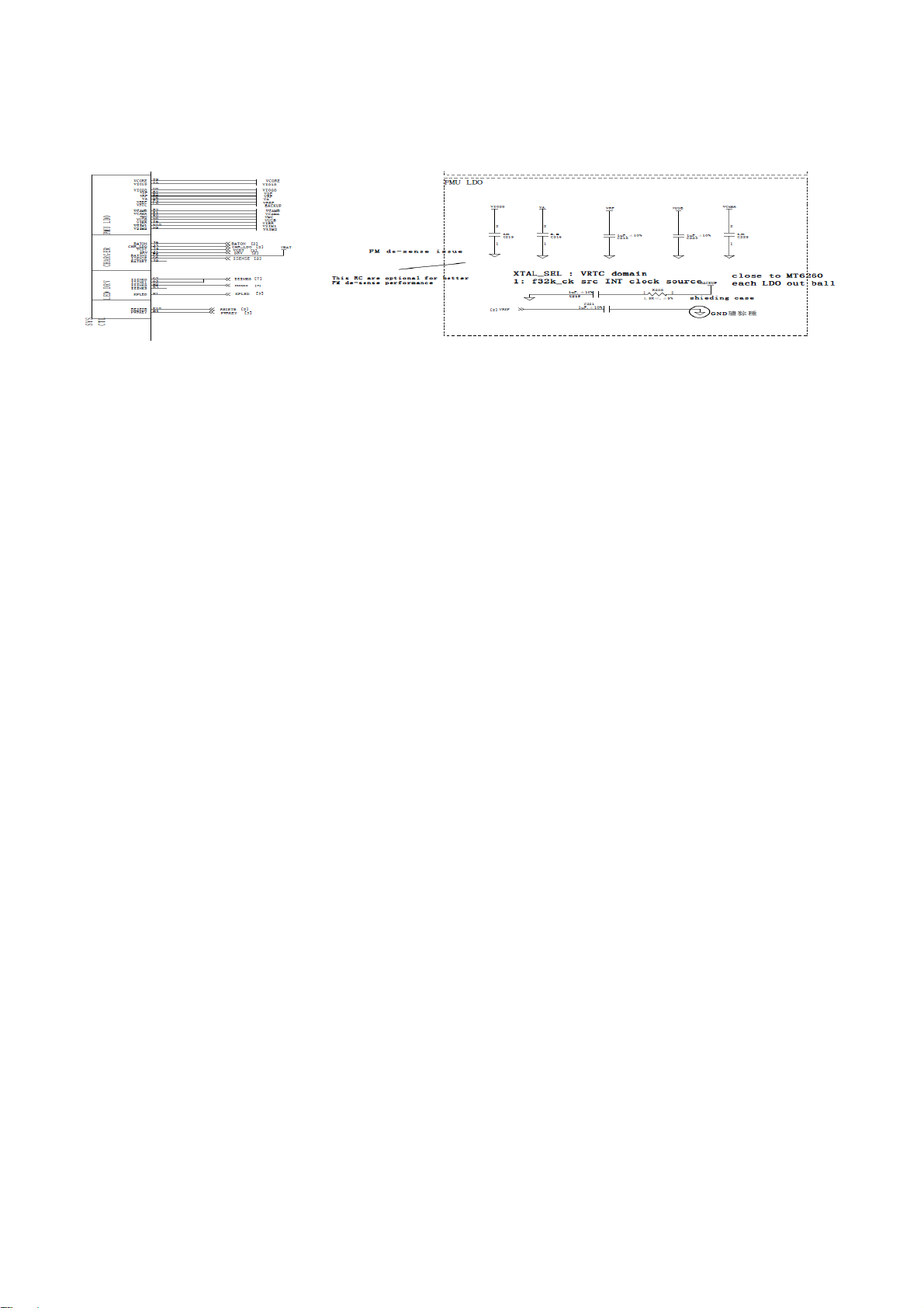
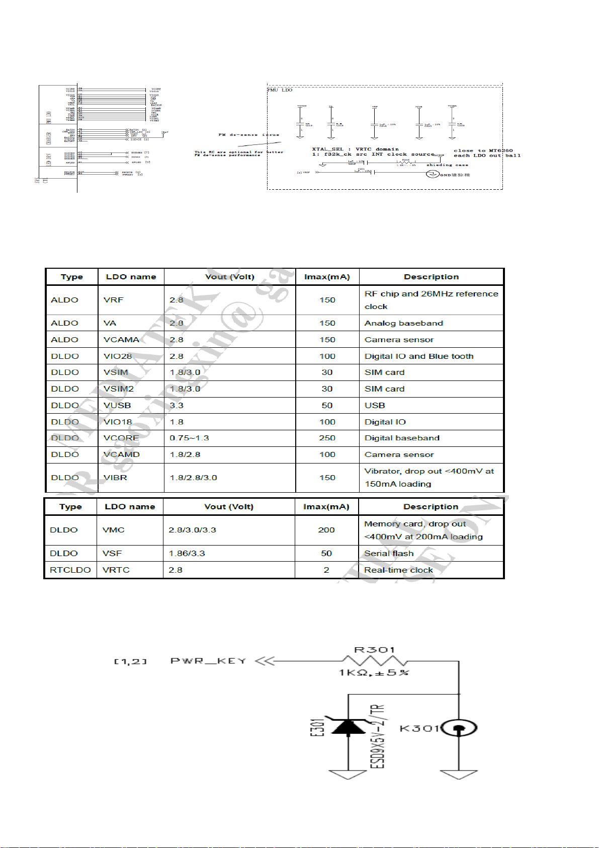
3.2.2 Explanation of power circuit and in-and-out circuit
Power source is provided by MTK MT6260 and periphery components, main function as below:
A. 2.8V-5.5V Input Range
B. Charger input up to 8V
C. Seven LDOs optimized for specific GSM Sub-systems
D. One LDO for RF transceiver
E. High operation efficiency and Low stand-by current
F. Li-Ion battery charge function
G. SIM Card interface
H. Two open-drain output switches to control the LED and vibrator
I. Three NMOS switches to control RGB LEDs
J. Thermal Overload Protection
K. Under Voltage Lock-out Protection
I. Over Voltage Protection
M. Power-on Reset and Start-up Timer
Page 12
1. power supply
high. At that time, the power
MT6260 power supply:
2、power on/off circuit
After the handset power off, the pin PWRKEY is pulled high. The pull-up resistance is
Page 13
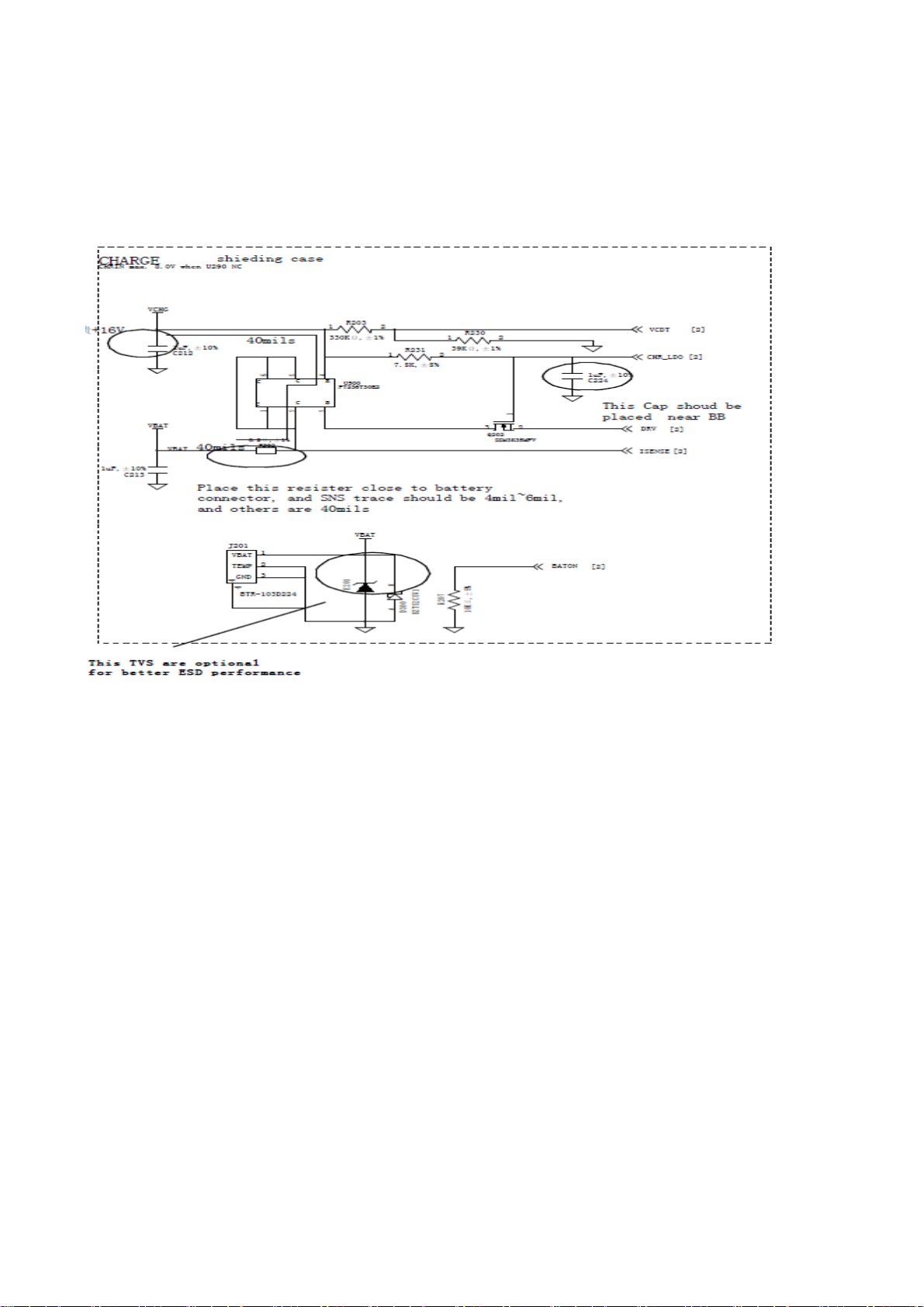
Charge Circuit
inside the chip .When the power key is pressed, the pin PWRKEY is pull low, then the
MT6260 turn on all the Power supply function and the baseband chip enter working status.
So the pin BBWAKEUP is pulled high. At that time, the power key can be released; the
CPU-baseband chip can control the MT6260 .
MT6260 charge
management function:
1、Charger detection
2、Battery voltage measurement
3、Charging current measurement
4、Over voltage Protection
5、Charge mode selection
MT6260 is available to control the pulsed charging current. The pin CHRIN is to detect the
Charger. The pins ISENCE/BATSENES can calculate the battery voltage by detect the voltage
of R400, and calculate the charge current by the voltage of the resistance R400. In different
charge mode, Baseband chip sent the different PWM pulse signal to MT6253, so the
MT6233Acan control the process of charge.
The charge process include three states: pre-charging mode, constant current
mode and constant voltage Mode. If the battery voltage is bellow 3.2V, the
handset enter pre-charging mode; If the battery voltage is over 3.2V, it enter the
constant current mode.
Page 14
.
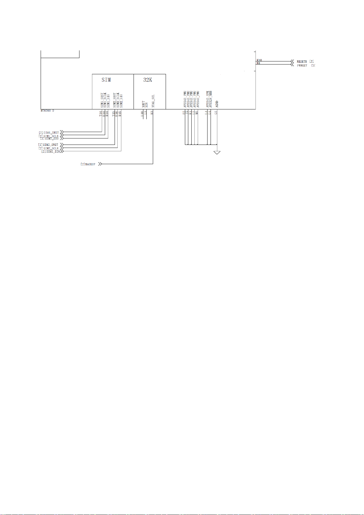
3.2.3 SIM interface
SIM interface circuit
The power management chip supply the interface between the SIM card and
baseband chip, the Key signal is: SIM_CLK (the clock signal), SIM_RST (the reset signal),
SIM_I/O (I/O signal), VSIM (SIM power supply).
3.2.4 Principle of audio frequency circuit
The Audio Frequency (AF) circuit includes three parts: RECEIVER and SPEAKERs,
HANDSET MIC, ERAPHONE and HANDFREE MIC.
the AF Signal to the AF amplifier though MP3_OUT port. After the AF signal is amplified, it goes to
the Speaker. The RECIEVER is drove by the baseband chip directly. As an electrets tone arm, the
MIC Needs power support when working. The MICBIASP/N port of the baseband chip supports bias
Voltage for Mic. The EARPHONE port is dual-used with the USB port. For more details Please
refer to "communication ports" in later part.
There are 4 speakers; each speaker is drove by an AF amplifier. The baseband chip sends
Page 15
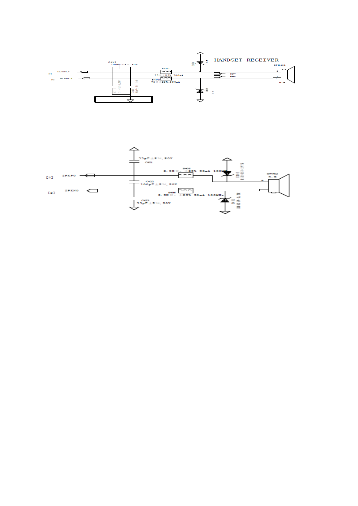
1、Receiver
Figure 3.2.5 Circuit of receiver
2、Louder speaker
Figure 3.2.6 Circuit of louder speaker
Page 16

3、Handset microphone Earphone
Figure 3.2.7 Circuit of MIC bias voltage circuit of mobile phone
4、Hands-free microphone
3.2.5 LCD circuit
Figure 3.2.8 Circuit of Hands-free microphone
Page 17

Memory and all the periphery equipments used the same bus based on the 1st generation
base band chip That made the system very slow. Considering that, MTK have altered the
hardware structure to separate The periphery equipments (like LCD and NAND etc.) from
memory bus and all of them use the System clock simultaneously
LCD use series type LCD and four control bus (LPCEOB_MAIN_LCM is chip select signal; LPA0 is
select bus for register and commend; LWRB is LCD writes strobe; LRDB is LCD read strobe, LRSTB
is reset signal. LCD is controlled by baseband IC.
Display data is transferred to video RAM in LCD driver by I/O port in DMA mode. So system Can
response quickly and multimedia runs fluently without mosaic or picture feeling. Three Commonanode LEDs in charge of background light supplying. Three voltage sensitive resisters are Needed
to protect the LCD from electrostatic harm and extend the life of LCD.
Figure 3.2.9 LCD interface circuit
Page 18

3.2.8 T-Flash circuit
T-Flash card interface: VDD is supplied by MT6260
3.2.10 FM
FM is integrated in MT6260.
Page 19

3.2.11 key interface
When key is pressed down, the matrix KCOLX status is pulled down to low. Interrupt occurs,
Then Baseband can judge the key's location, so system implements corresponding function.
Page 20

Chapter 4: Failure Analysis
The main fail cases:
Fail to download; Fail to power on; Fail to make a call (due to RX or TX); Fail to charge; RX/TX
power fail; Audio malfunction; No vibration; No display; Power supply fail; SIM check fail and so on.
In mobile circuit system, all the electrical connecting trace can be divided into three types, such
As power supply trace, controlling trace and signal trace. When analyzing the RF failure case, for the
Active circuit we should first check the power supply, then control circuit followed by the signal flow
Path to remove the failure step by step. When debugging the RF malfunction, we should diagnose the
RX part first before TX.
With the help of oscilloscope we can diagnose power supply issue, control signal trouble and
Some low frequency signals, such as I/Q signal, RTC signal, crystal oscillator signal and so on. We can
Measure the signal features such as amplitude, frequency, duty cycle etc. We can also use millimeter
to measure power supply DC voltage. For RF signal, we usually use spectrum analyzer to check signal
Spectrum and amplitude in frequency domain.
We provide a useful phone maintain software - META. Some introduction about META will be
Showed below.
4.1 Analysis of base band failures
4.1.1 The handset can not be power on
Transceiver (MT6260), 26MHZ VC TCXO, 32KHZ crystal. you can measure the voltage according with
3.2.2 . Then measure if the 26MHZ,32KHZ output the CLK signal with right frequency to baseband, if no fault
occurs, continue to check FLASH, basebandMT6260chip by download a code, if can download DA, indicate
baseband is normal, otherwise re-soldering the baseband chip and memory .replace these chips if all the step
can't solve the fault.
Interrelated components are mainly as below: PMIC, Baseband chip (MT6260),MCP Flash,RF
4.1.2 Display failure
FLY Ezzy5 is a bar phone, LCM is soldering on the PCB directly. A bad soldering can lead to display
Failure, you can check it with your eyes or measure the PIN with digital millimeter, if the soldering is OK,
maybe it is the problem of LCM or MAINPCBA. You can change the LCM or repair the
MAIN PCBA.
Page 21

4.1.4 Keys failure
Key circuit is simple, check the net is short or not. If the issue is still there, you need to check
The BB chip at last.
4.1.5 Voice cannot be sent or received
This often occurs in a mobile phone. You can enter into engineering mode by inputting *#2233*#
First you go to the test item "receiver", and then you can hear "du du" sound if the receiver is good.
Otherwise you need to test its resistance with millimeter. It should be 32ohm. If the resistance is much
bigger it means the receiver is bad, so you can change for a good one. Second you go to the test item
"echo" and test MIC. Huff at MIC then there will be an echo at receiver that shows the microphone is
ok. Otherwise you must check the microphone bias circuit, test bias voltage and output signal,
Microphone resistance should be 2.2k OHM.
4.1.6 No voice in speaker
First you can check if the audio source can output from baseband chip with a headset. Then check
speaker resistances see if it's 8ohm or not. If not, the speaker is bad. Otherwise you need to check
audio PA circuit. After repaired, you can test it on engineering mode again.
4.1.8 T-Flash card failure
T-Flash card circuit is very simple, so you must pay more attention to card socket to see if it is
Soldered well.
4.1.9 Cannot download software
There are many reasons that can lead to download failure, but the problem of the analog switch
IC, Which is used to control the dual-used port by headset and UART, is the most common. So you
need to Pay more attention to it.
4.2 Analysis of RF failure
RF failure often occurs in calibration or capability test, the best diagnostic method is to use
Wireless universal tester, spectrum analyzer and signal source matched with META tool to test it.
Corresponding components with the RF receiving mainly are: antenna switch saw filters,
matching circuit etc. You need to check if one of them is bad soldering or damaged. If power received
is too low maybe the RF circuit is cut off, you need to check saw filter, matching circuit, and antenna
Switch and control signal etc. If the bit error is too high, it may be because the saw filter is not
Qualified.
RF transmitting circuit associated components is mainly as below: base band MT6260, RF
Transceiver MT6260, attenuator, RF PA, antenna switch etc, main test items including power value
power vs. time, modulation and switch spectrum etc. The current consumption when transmitting RF
signal is about 200 mA. So if the current is too low, it means the PA doesn't work properly, you need
to change it for a new one.
Page 22

Chapter 5: Manual of tool software
5.1Flash Tool
Notice: Before you go for the software download process, please make sure you have installed the
download driver for your PC already.
Step 1: Open “Flash -tool” , then the opened windows is as
following:
Step 2: Click on the button , then chose from
the flash tool file .
Page 23

Step 3: Click on the button , then chose the “cfg” file from the software file which need
to be downloaded.
Step 4: Click on the button ,and the windows is as following:
Page 24

Step 5: Insert the download cable to your PC。
Step 6: Now make sure the battery in the phone but not turn on,then long press (keypad 3
button )and insert download USB to the phone till you see the red bar appear,then
you no need press keypad 3 button.(Here is very important,must press keypad 3 button till you see
the red bar)
Step 7: The end. There will be displayed on the PC which means the software is well
download.
Page 25

If you can not download, please check if you have install USB driver successful.
When need to download software
· Upgrade software to higher version. Bugs of function and performance will appear
during Using the handset. To improve the function and performance of the handset,
the Manufacturer will improve the software and release new software version. Users
can download new version to improve the function and performance of the handset.
· Program errors or disorder because of improper setting by users, e.g. the
handset can't power on, or being locked, and so on.
· In principle, it is not allowed to download a software lower than the current version,
unless It's specified.
Caution: Before downloading software, please save all information and phone numbers
in the handset. After the software is downloaded, the handset will delete all the
information and
restore to the factory default software environment.
5.2 CKT maintain software introduction -META
5.2.1 META-RF TOOL
Step 1. Open Maui META and select correct COM port ,META status window shows' Please
reset target' ,otherwise if it is in' Connect with target' status, please click 'Reconnect'。
Page 26

Step 2: Connect the download cable between the corresponding computer COM port and the
target MS. Then power on the mobile .At this time META will detect the mobile and order the
mobile into META mode. The META status window will then change to 'Connect with target'.
And then you may select RF Tool from the pull down menu. Just pop up the RF tool option
group as below:
Page 27

Testing result of Power
5.2.2 The features of META RF Tool PM
PM is used for measuring the receiver Rx level at a given RX
channel:
Page 28

At first you should configure the Universal wireless communication tester such as Agilent 8960 or R&S
CMU200 please follow the below picture for your configuration guide:
In META page PM, please click RX Path Loss Setting into AGC PATH LOSS setting page. Click
Upload from flash button to read the RX path loss parameter form the mobile. If you have not loaded
the correct database file yet, META will notice you to open a database. Please follow it and then you
will see the target RX path loss parameters for different channels in the AGC path loss window.
Please note that all the RX loss values should be in the tolerance range of +/-5dB, otherwise it
Should be a hardware failure.
Page 29

Follow below settings and press 'start' button to active RX measurement. Due to the System
simulator (8960) downlink Cell power is -70dbm,The Ant power reported from the mobile
should
be about -70dbm, tolerance+-5dB. Otherwise it means there is some defect with RX path. Please
Check the GSM RX SAW and the surrounding circuit, like ASM and RF test connector.
For DCS/PCS band, do the same operation except for the band select and the 8960 band
settings. Note that the ARFCN should be the same setting as the 8960 Broadcast chan.
Page 30

TX level and profile is intended for checking the Transmitter's output power, ramping profile at a
TX level and profile
TSC 为5
given channel and power control level.
RF Tool TX level and profile
Set the 8960 to non-signal mode
Page 31

Set Expect burst TSC code of 8960 the same as META indicated.
CONFIDENTIAL
Set 8960 Traffic band for EGSM, Traffic Channel to 20,MS TX Level:5 and wait for
receiving
Page 32

the MS burst.
Press GMSK level and ramp setting button into GMSK APC profile setting page:
Page 33

Follow below setting page the set the corresponding TX parameters:ARFCN, TSC, PCL DAC
etc. Then click Start button to start transmitting burst.
Page 34

If the Target MS' TX function is OK you may see a TX PVT profile from the 8960 as follows:
Page 35

If you can not see anything or it shows fail in the 8960's PVT window, please follow below debug
wizard to check and remove all the failure about TX path.
1. First of all we use oscilloscope to check PA TX enable control signal waveform:PA_EN, The normal case
shows below; Otherwise please check Baseband circuit.
Page 36

2. PA Vapc control signal waveform :VAPC (GSM LEV5)
Chapter 6: Tools List
6.1 Downloading Operation Manual
Reference: Flash_tool.exe
6.2 Write SN Operation Manual
Reference: IMEI Writing Manual
6.3 Calibration Operation Manual
Reference: Maui
Page 37

1 2 3 4 5 6 7 8 9 10
H
G
CAMERA
47KΩ,±5%
F
E
D
[1]CMRST
R104
VIO28
n.mR103
R102
[1]CMPDN
CMPDN(HW trapping PIN):
VSF POWER SEL.
100KΩ,±5%
0: 1V8
1: 3V3
CMRST(HW trapping PIN):
USB 2VCOM
0: disabled(default)
1: enabled
[7]
[7]
[7]
[7]
[7]
[7]
[7]
[7]
[7]
[7]
[7]
[7]
[3]MCCM0
[3]MCCK
MCDA0
[3]
[3]MCDA1
[3]MCDA2
[3]MCDA3
[2]SQI_SI
[2]
SQI_CE
[2]
SQI_SO
[2]SQI_SCK
SQI_SIO3
[2]
[2]SQI_SIO2
[7]
LPA0
LRD_B
LWR_B
LPCE0_B
LPRSTB
NLD0
NLD1
NLD2
NLD3
NLD4
NLD5
NLD6
NLD7
[3]KROW3
[3]KROW2
[3]KROW1
[1]CMRST
[1]CMPDN
U101-A
C15
CMDAT7
D12
CMDAT6
A15
CMDAT5
B15
CMDAT4
B13
CMDAT3
C13
CMDAT2
E12
B14
CMDAT1
A14
CMDAT0
CMPDN
A18
E18
F17
C18
C17
C14
C16
D18
D17
E11
B16
A17
A12
B12
KCOL1
KCOL2
KCOL3
KCOL4
KROW0
KROW1
KROW2
KROW3
CMPCLK
CMMCLK
CMVREF
CMHREF
KROW4
CMRST
[3]KROW0
[3]KCOL4
[3]KCOL3
[3]KCOL2
[3]KCOL1
[3]KCOL0
E17
KCOL0
CAMERA KEY
P19
MCINS
T17
MCCM0
U18
MCCK
T16
MCDA0
T18
MCDA1
U17
MCDA2
R17
MCDA3
T19
SOUT
P18
SFCS0
R19
SIN
N16
SCK
P17
SHOLD
N17
SWP
R18
SFCS1
J16
LSCE1_B
H18
LSRSTB
J17
LPTE
K16
LPA0
L17
LRD_B
L16
LWR_B
LCM MSDC
L18
LPCE0_B
M17
LPCE1_B
K18
LPRSTB
G17
NLD0
G16
NLD1
H17
NLD2
J18
NLD3
K17
NLD4
N18
NLD5
K19
NLD6
H16
NLD7
J19
VIO28
B9
NLD8
DVDD28_FSRC
MT6260 D
MT6260 D/M/S_BB
SYS_CTL
WATCHDOGJ9SRCLKENAIG4TESTMODE
F16
GND
GND
GND
GND
GND
GND
GND
GND
GND
GND
GND
G12
J12
G19
J10
H11
A19
M18
M19
U12
U19
G10
Other
interface
UARTI2C
TPUSBADC
GPIO16
GPIO17
GPIO19
EDIDAT
USB11_DM
USB11_DP
AUX_IN4
B10
UTXD1
C11
URXD1
B11
UTXD2
A11
URXD2
D16
SCL28
F18
SDA28
B19
B18
B17
D19
EDIWS
F19
C19
EDICK
T4
XM
U3
YM
R3
XP
T3
YP
U13
T13
R1
[2]UTXD1
[2]
URXD1
[3]GPIO61_EINT8_SOS
[4]USB_DM
[4]USB_DP
H
G
F
E
D
C
B
A
PDF 文件使用 "pdfFactory Pro" 试用版本创建 www.fineprint.cn
MediaTek Inc.
Title
MT6260
Document Number
Size
A1
Baseband
Thursday, January 03, 2013
MediaTek Confidential
No.1-2, Innovation Rd 1, SBIP, Hsin-Chu City 300
TEL:(03)567-0766 FAX:(03)578-7610
Drawn
ofSheetDate:
10987654321
C
B
A
Rev
1A
71
Page 38

1 2 3 4 5 6 7 8 9 10
H
VBAT IN
G
F
shieding case
POWER IN , SF POWER , PSRAM POWER
VCORE
E
D
VIO28
VIO18
VMC
VSF
SIM
C
B
A
VBAT
VBOOST
C201
2.2uF,±10%
charge pump close to MT6260
C207
C205
1uF,±10%
1uF,±10%
close to MT6260 each power in ball
1uF,±10%
1uF,±10%
C202
1uF,±10%
C203
C204 1uF,±10%
C206
close to MT6260 each power in ball
VBAT
C209 1uF,±10%
1uF,±10%
C301
[3] PWR_KEY
2.2uF,±10%
C210
MP Test Points
UART1 & PWR & SIM
[1]UTXD1
URXD1
[1]
VSIM2
[2]SIM2_SIO
C331
VCDT
DRV
ISENSE
ISINK0
ISINK2
KPLED
[2]
RESETB
WSON type
U203
MX25U6435EZNI-10G
5
DI_DQ0_
2
DO_DQ1_
3
WP#_DQ2_
7
NC_DQ3_
1uF,±10%
Charge Pump
[2]
FLYN
[2]
FLYP
Vibrator
[2]
VIBR
1uF,±10%
C214
VCORE
VIO18
VIO28
VSF
VRF
VA
VREF
BACKUP
VCAMD
VCAMA
VMC
VUSB
VIBR
VSIM1
VSIM2
[2]BATON
[2]CHR_LDO
VBAT
[2]
[2]
[2]
[7]
[7]
[3]
[3]PWRKEY
VSF
8
VCC
1
CS#
6
CLK
4
VSS
GND
9
FM de-sense issue
This RC are optional for better
FM de-sense performance
C228
100nF±5%,50V
[1]SQI_CE
[1]SQI_SCK
PMU LDO
VIO28
2
1
VREF
[2]
CHARGE
CHRIN max. 8.0V when U290 NC
VCHG
瑻溃+16V
1uF,±10%
C212
VBAT
40mils
VBAT
1uF,±10%
C213
Place this resister close to battery
connector, and SNS trace should be 4mil~6mil,
and others are 40mils
This TVS are optional
for better ESD performance
All Charge Pump GND "Must Be" directly to
a non-fractured GND plane !!
25mils
25mils
25mils
25mils
4.7uF,±10%
C217
4.7uF,±10%
C220
VBATVBOOST
shieding case
R213
0Ω,±5%
n.m
C215
XTAL_SEL : VRTC domain
1: f32k_ck src INT clock source
J202
1
n.m
MOT+
2
MOT-
VA
VRF VUSB
2
n.m
1uF,±10%
C216
1uF,±10%
C219
C221
1uF,±10%
C218
R208
1 2
1.5KΩ,±5%
1
shieding case
R203
2
J201
VBAT
TEMP
40mils
0.2Ω,±1%
GND
4
4
BTR-103D224
1
330KΩ,±1%
52
C
E
C
C B
C
1 6
3 4
R202
1
2
3
U500
PT236T30E2
R230
1 2
39KΩ,±1%
R231
1 2
7.5K,±5%
Q202
SSM3K35MFV
VBAT
E201
R207
A K
10KΩ,±5%
D300
BZT52C5V1
4.7uF,±10%
C222
Three CAP
close to MT6260
VCAMA
2
n.m
1uF,±10%
C225
C223
1
close to MT6260
BACKUP
each LDO out ball
shieding case
GND璶猔種
[2]VCDT
[2]CHR_LDO
1uF,±10%
C224
This Cap shoud be
1
placed near BB
23
DRV
[2]
ISENSE
[2]
BATON
[2]
MediaTek Confidential
MediaTek Inc.
Title
Size
A1
Date: Sheet of
No.1-2, Innovation Rd 1, SBIP, Hsin-Chu City 300
TEL:(03)567-0766 FAX:(03)578-7610
MT6260
Document Number Rev
PMU
Thursday, January 03, 2013
Drawn
10987654321
2 7
H
G
F
E
D
C
B
A
1A
C330
C226
33pF±5%,50V
P2
AU_MICBIAS1R2AU_MICBIAS0
[2]SIM1_SIO
T1
AU_VIN0_PU1AU_VIN0_NU2AU_VIN1_PT2AU_VIN1_N
AUDIO
R5
HSNT5HPLP5HSPU5HPR
VSIM1
[2]SIM2_SCLK
[2]SIM2_SRST
C227
1uF,±10%
33pF±5%,50V
M2
K1
L2
FLYNK2FLYP
VBOOST
SPK_OUTNM1SPK_OUTP
Charge pump
[2]SIM1_SCLK
[2] SIM1_SRST
33pF±5%,50V
MICBIAS1
MICBIAS0
VBAT
VBOOST
VBAT
VCORE
VIO28
VIO28
VMC
VSF
VIO18
JS201
1
I/O6CLK
2
5
VPP
RST
3
4
GND
VCC
C231
C230
33pF±5%,50V
[4]
SPKN0
[4]
SPKP0
[4]
MP3_OUTR
[4]
MP3_OUTL
[4]
AU_OUT0_P
[4]
AU_OUT0_N
[4]
MICN1
[4]
MICP1
[4]
MICN0
[4]
MICP0
[4]
ACCDET
F10
K12
D14
R16
M16
F14
F15
U9
M3
E3
A9
U101-B
VBAT_DIGITAL
VBAT_SPK
VBAT_VA
VDDK
VDDK
DVDD28
DVDD28
DVDD33_MSDC
DVDD28_SF
DVDD18_EMI
DVDD18_EMI
N3
ACCDET
POWER IN VBAT IN
MT6260 D/M/S_ABB
SF
POWER
PSRAM
POWER
SIM 32K
XTAL_SELL9XIN
XOUT
SIM1_SCLK
SIM1_SRST
SIM1_SIO
SIM2_SCLK
SIM2_SRST
MT6260 D
[2]SIM1_SRST
[2]SIM1_SCLK
[2]SIM1_SIO
[2]SIM2_SRST
[2]SIM2_SCLK
[2]SIM2_SIO
1
TP201
1
TP202
1
TP203
1
TP204
1
TP205
SHOLD : SIO3
SWP : SIO2
SOUT : SQI_SI : DQ0
SIN : SQI_SO : DQ1
SIM2_SIO
L10
U14
T14
R14
U16
T15
R15
[2]BACKUP
SYSTEM CONTROL
[2]RESETB
This Cap shoud be placed near BB
This CAP(330pF) are optional
for better ESD performance
K9
1KΩ,±5%
C232
K4
AVSS43_CPL3AVDD43_CP
AVSS43_PMUJ7AVSS43_PMUE5AVSS43_PMU
AVSS43_PMUM6AVSS43_PMUU4AVSS28_ABB
K7
L5
VIO28
C229
33pF±5%,50V
SYS
AGNDL4AVSS43_SPK
G5
JS102
5
RST
4
VCC
LED DRV PMU LDOCHARGER
CTL
I/O6CLK
VPP
GND
CHR_LDO
1
2
3
33pF±5%,50V
VBOOST
[2]FLYN
[2]FLYP
VBAT
T9
VCORE
T8
VIO18
U8
VIO28
R7
VSF
E2
VRF
U6
VA
F4
VREF
L8
VRTC
F2
VCAMD
E1
VCAMA
R8
VMC
N8
VUSB
T6
VIBR
N10
VSIM1
N9
VSIM2
J6
BATON
J3
J4
VCDT
J1
DRV
F6
BATSNS
G6
ISENSE
J2
BATDET
G2
ISINK0
G3
ISINK1
H2
ISINK2
H3
ISINK3
H1
KPLED
K10
RESETB
H4
PWRKEY
[1]SQI_SI
[1]SQI_SO
[1]SQI_SIO2
[1]SQI_SIO3
PDF 文件使用 "pdfFactory Pro" 试用版本创建 www.fineprint.cn
Page 39

1 2 3 4 5 6 7 8 9 10
H
G
F
E
D
C
B
A
[1]
[1]
[1]
[1]
[1]
[2]PWRKEY
KCOL4
KCOL3
KCOL2
KCOL1
KCOL0
KROW0
[1]
KROW1
[1]
KROW2
[1]
KROW3
[1]
PWR_KEY
[2]
R301
1KΩ,±5%
E301
n.m
Keypad LED
VMC
n.m
K303
K304
K305
K302
n.m
E302
K301
GPIO61_EINT8_SOS
[1]
K310
K313
K308
K309
K311
K312
K314
K315 K318
K306
n.m
n.m
E303
n.m
E306
1 2
KEY301
KEY_ST-1185S
n.m
E307
E304
VIO28
R302
100KΩ,±5%
n.m
E305
E309
K316K307
n.m
E310
K317
n.m
E311
J303
n.m
VBAT
R303
390Ω,±5%
390Ω,±5%
n.m
E308
D301
AOT-0603W331A-NO-X-3
CON301
1
2
n.m
[2]KPLED
E312
D302
AOT-0603W331A-NO-X-3
n.m
[1]MCDA2
[1]MCDA3
[1]MCCM0
[1]MCCK
[1]MCDA0
[1]MCDA1
C302
100nF±5%,50V
R304
R305
390Ω,±5%
D303
AOT-0603W331A-NO-X-3
R308
390Ω,±5%
D304
AOT-0603W331A-NO-X-3
J301
1
DAT2
2
DAT3/CD
3
CMD
4
VDD
5
CLK
6
VSS2
7
DAT0
8
DAT1
R310
390Ω,±5%
D305
AOT-0603W331A-NO-X-3
10987654321
GND10DET11DET12GND
9
R311
390Ω,±5%
D306
AOT-0603W331A-NO-X-3
R312
390Ω,±5%
D307
AOT-0603W331A-NO-X-3
R313
390Ω,±5%
D308
AOT-0603W331A-NO-X-3
MediaTek Confidential
MediaTek Inc.
Title
MT6260
Document Number
Size
A1
KEY_SIM_T
Date: Sheet of
Thursday, January 03, 2013
No.1-2, Innovation Rd 1, SBIP, Hsin-Chu City 300
TEL:(03)567-0766 FAX:(03)578-7610
Drawn
3 7
H
G
F
E
D
C
B
A
Rev
1A
PDF 文件使用 "pdfFactory Pro" 试用版本创建 www.fineprint.cn
Page 40

1 2 3 4 5 6 7 8 9 10
HGFEDCB
A
MICBIAS1
1KΩ,±5%
R409
C499
100pF±5%,50V
C498
33pF±5%,50V
10uF,±10%
47KΩ,±5%
籔HeadSet(J5) 辅 翴 钡 钡╰参
R410
C410
10uF,±10%
1.5KΩ,±5%
XMIC
[4]
C497
100pF±5%,50V
C496
33pF±5%,50V
C411
33pF±5%,50V
12
R414
470KΩ,±5%
VIO28
AU_OUT0_P
[2]
AU_OUT0_N
[2]
HANDSET MICOPHONE
near BB located in
Shielding case
MICP0
[2]
MICN0
[2]
L401
0Ω,±5%R408
C413
100pF±5%,50V
C412
33pF±5%,50V
SPKP0
[2]
SPKN0
[2]
MICBIAS0
R500
1KΩ,±5%
R499
C414
100nF,±10%
1.5KΩ,±5%
B403
+
1
75Ω±25%_300mA
2
C418
C417
10uF,±10%
C415
100nF,±10%
1.5KΩ,±5%
1KΩ,±5%
XMP3_L
XMP3_R
C416
33pF±5%,50V
R498
R497
[4]
[4]
B402
75Ω±25%_300mA
33pF±5%,50V
100pF±5%,50V
C423
33pF±5%,50V
75Ω±25%_300mA
C421
C422
100pF±5%,50V
75Ω±25%_300mA
33pF±5%,50V
钡 癬 辅╰参
B404
C419
B401
B405
2.5KΩ。±25% 50mA 100MHz
B406
2.5KΩ。±25% 50mA 100MHz
E412
C420
33pF±5%,50V
HANDSET RECEIVER
n.m
E404
E403
n.m
E503
E402
E401
ESD9X5V-2/TR
MIC401
n.m
RCV+
RCV-
ESD9X5V-2/TR
+
B407
XMP3_R
[4]
XMP3_L
[4]
XMIC
[4]
SPK401
2
1
+
n.m
SPK402
n.m
2.5KΩ。±25% 50mA 100MHz
B408 2.5KΩ。±25% 50mA 100MHz
[1]
[1]
B409
75Ω±25%_300mA
FM_LANT
USB_DP
USB_DM
VCHG
ESD5V3U1U-02LRH
E501
ESD9X5V-2/TR
E499 ESD5V3U1U-02LRH
E502
E500
ESD9X12ST5G
R496
FM_ANT-P
[5,6]
[5,6]
0Ω,±5%
B410
R495
FM_ANT-N
0Ω,±5%
HEADSET MICOPHONE
near BB located in
Shielding case
H
MICN1
[2]
MICP1
[2]
G
ACCDET
[2]
HEADSET EarPhone
F
MP3_OUTL
[2]
MP3_OUTR
[2]
E
D
C
B
A
C401
100nF,±10%
C408
100nF,±10%
C502
1KΩ,±5%
R405
HOOK DETECTION
near BB located in
Shielding case
R401
100Ω,±5%
R402
100Ω,±5%
HEADSET DETECTION
EAR_EINT
[5]
HANDSET RECEIVER
33pF±5%,50V
C501
10uF,±10% C500
E496
E498
ESD9X5V-2/TR
ESD9X12ST5G
VCHG
J404
100nH,5%
E497
ESD9X5V-2/TR
n.m
MediaTek Confidential
No.1-2, Innovation Rd 1, SBIP, Hsin-Chu City 300
MediaTek Inc.
TEL:(03)567-0766 FAX:(03)578-7610
Title
MT6260
SizeDocument Number
A1
AUDIO&IO
Date: Sheet of
Thursday, January 03, 2013
7
GND
6
UTXT
5
VBAT
4
D+
3
D-
2
URXT
1
VCHG
UAF95-07254-1510-B
1
DC+
2
DC-
8
GND9GND10GND11GND12GND13GND
Drawn
J401
J402
n.m
J403
n.m
Rev
1A
4 7
10987654321
PDF 文件使用 "pdfFactory Pro" 试用版本创建 www.fineprint.cn
Page 41

1 2 3 4 5 6 7 8 9 10
Shieding ず all RF sheet
H
This pairs of RC-filter are optional
for better RF de-sense performance
ANT600
G
F
E
D
ANT599
n.m
n.m
J700
1TEST
2 GND
12
RX1
13
VBAT
C522
22uF,±20%
NC
14
ANTENNA
15
GND
16
GND
17NC19
C504
3.9nH
C505
C503
n.m
n.m
C595 22pF,±5%
C596
22pF,±5%
7
10NC11
RF7176D
GND8GND9GND
6
GND
U501
5
RFIN_LB
4
GND
3
RFIN_HB
2
GND
1
GND
GND
23
C590
220pF±5%,50V
RX0
VBATT
18
GPCTRL120GPCTRL021TX_ENABLE22VRAMP
FREF trace as short as possible, need shielding
[5]RXLB_P
[5]RXHB_P
R509
10KΩ,±5%
R507
24KΩ,±5%
[5]TX_EN
[5]BANDSW
[5]TR_SW_EN
[5]TXO_LB
[5]TXO_HB
APC_VBIAS
VA
VCAMA
[5]APC_VBIAS
[5]BANDSW
BPI_BUS1
[5]TX_EN
[5]TR_SW_EN
[5]RXLB_P
[5]RXHB_P
[5]TXO_LB
[5]TXO_HB
[5]
F9
T12
P1
C10
C9
D9
D11
A2
A3
B1
B2
C1
C2
U101-C
AVDD28_2GAFE
AVDD28_FM
APC
BPI_BUS0
BPI_BUS1
BPI_BUS2
BPI_BUS3
RXLB_P
RXLB_N
RXHB_P
RXHB_N
TXO_LB
TXO_HB
MT6260 D
POWER INGSM
MT6260 D/M/S_RF
AVSS_2GA5AVSS_2G
A1
C5
AVSS_2GC3AVSS_2GD2AVSS_2GD4AVSS_2G
D1
E7
AVSS_BT connected together then connect to main ground.
TP3B5TP4B4TP2C4TP1
AVSS_2G
[4]EAR_EINT
BTFM
B8
BT_LNA
U11
FM_ANT_P
T11
FM_ANT_N
26M &
CLK BUFFER
A6
XTAL1
B6
XTAL2
D6
FREF1
C7
CLK_SEL
AVSS_FMC8AVSS_BTB7AVSS_BT
T10
[6]BT_LNA
[4,6]FM_ANT-P
All block close to MT6260
[4,6]FM_ANT-N
26M
1
2
」 DCXO(X'tal) : CLK_SEL= GND_RF
」 Co-clock(ext CLK) : CLK_SEL= DVDD28_IO
GND
GND3HOT
X502
XTL571100-M118-015
4
GND
H
G
F
E
D
C
B
A
POWER IN
VCAMA
VA
1uF,±10%
C586
close to MT6260 each power in ball
PDF 文件使用 "pdfFactory Pro" 试用版本创建 www.fineprint.cn
This R is optional
for better FM de-sense performance
1uF,±10%
C585
MediaTek Confidential
MediaTek Inc.
Title
Document Number
Size
A1
Date: Sheet of
No.1-2, Innovation Rd 1, SBIP, Hsin-Chu City 300
TEL:(03)567-0766 FAX:(03)578-7610
MT6260
RF
Thursday, January 03, 2013
Drawn
5 7
10987654321
C
B
A
Rev
1A
Page 42

1 2 3 4 5 6 7 8 9 10
H
BT_LNA
[5]
G
These two cap are optional for better BT performance (Matching)
F
E
D
50ohm
R602
0Ω,±5%
Close to IC
3.9pF±5%,50V
L601
0Ω,±5%
C601
10pF,±5%
ANT601
n.m
C602
10pF,±5%
R605
H
0Ω,±5%
C603
1.5nH
L602
C604
n.m
For BT ANT matching
C605
n.m
G
F
PASS SIG spec must need LC filter
E
ANT702
n.m
D
C704
n.m
R702
470nH
C705
2.7pF±0.25pF,50V
[4,5]
FM_ANT-P
C
FM_ANT-N
[4,5]
B
A
PDF 文件使用 "pdfFactory Pro" 试用版本创建 www.fineprint.cn
C
R703
0Ω,±5%
B
MediaTek Confidential
MediaTek Inc.
Title
MT6260
Document Number
Size
A1
BT FM
Date: Sheet of
Thursday, January 03, 2013
No.1-2, Innovation Rd 1, SBIP, Hsin-Chu City 300
TEL:(03)567-0766 FAX:(03)578-7610
6 7
10987654321
Rev
0C
Drawn
Kenny Wu
A
Page 43

5 4 3 2 1
D
J903
n.m
1
GND
2
VCC
3
IOVCC
4
DB7
5
DB6
6
DB5
7
DB4
8
DB3
9
DB2
10
DB1
11
DB0
12
RD
13
WR
14
RS
C
RESET
LEDK
LEDA
15
16
CS
17
18
19
GND
20
NC
21
NC
22
NC
NLD6
NLD3
NLD2
ISINK0
[1]NLD5
[1]NLD1
[1]NLD0
[1]LPA0
[1]NLD7
[1]
[1]NLD4
[1]
[1]
[1]LRD_B
C906
C904
100nF,±10%
[1]LWR_B
[1]LPRSTB
[1]LPCE0_B
[2]
VBAT
4.7uF,±10%
B
VIO28
VIO18
C905
100nF,±10%
K701
STP 1290H
GND15GND2
4
J702
VBAT
n.m
C706
4.7uF,±10%
6
R
GND37GND4
3
COM
2
L
1
R704
390Ω,±5%
J703
n.m
R701
0Ω,±5%
D
C
B
[2]ISINK2
A
PDF 文件使用 "pdfFactory Pro" 试用版本创建 www.fineprint.cn
MediaTek Confidential
MediaTek Inc.
Title
MT6260
Document Number
Size
A1
LCD&CAM
Date: Sheet of
Thursday, January 03, 2013
No.1-2, Innovation Rd 1, SBIP, Hsin-Chu City 300
TEL:(03)567-0766 FAX:(03)578-7610
Drawn
7 7
12345
A
Rev
1A
Page 44

PDF 文件使用 "pdfFactory Pro" 试用版本创建 www.fineprint.cn
Page 45

PDF 文件使用 "pdfFactory Pro" 试用版本创建 www.fineprint.cn
Page 46

PDF 文件使用 "pdfFactory Pro" 试用版本创建 www.fineprint.cn
Page 47

PDF 文件使用 "pdfFactory Pro" 试用版本创建 www.fineprint.cn
Page 48

PDF 文件使用 "pdfFactory Pro" 试用版本创建 www.fineprint.cn
 Loading...