

Fly EZZY4 Service Manual

.
FLY
SERVICE MANUAL
EZZY4

CONTEANT LIST
Chapter 1: Summary
Chapter 2: Exploding Diagram
Chapter 3: Explanation of Schematic
Chapter 4: Failure Analysis
Chapter 5: Manual of tool software
Chapter 6: Tools List
Chapter 1: Summary
This streamline and comfortable handset is a perfect combination of humanized design and
Excellent craft. Besides the basic call function, FLY provides you with a collection of practical
Functions including sweet ring tone, cartoon incoming-call animation, File manager
(T-Flash card support). It also supports MMS and increment service which facilitate your work and
entertainment.
EZZY 4
In order to support technicians to be familiar with FLY handset, please master the method of servicing.
In addition, we provide corresponding technical data, including CKT base band, RF and software. There are
also many base band and RF test reference points and description of circuit. You can refer to maintaining
examples. Hope it could give you some help.
Main specification and technique standards of FLY are as below:
Standby time:
Talking time:
Style of network
EZZY 4
EZZY 4
240~312 hours
420~600 Minutes
GSM900, DCS180
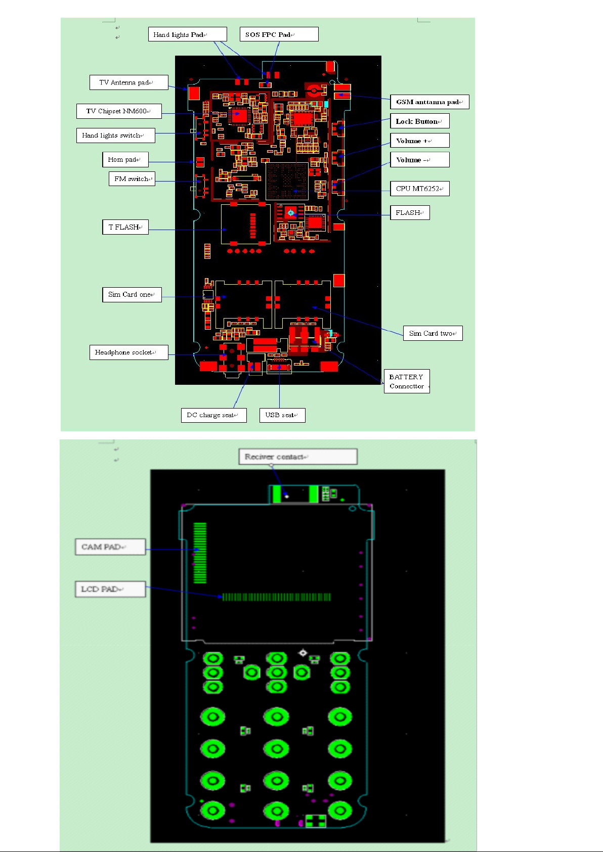
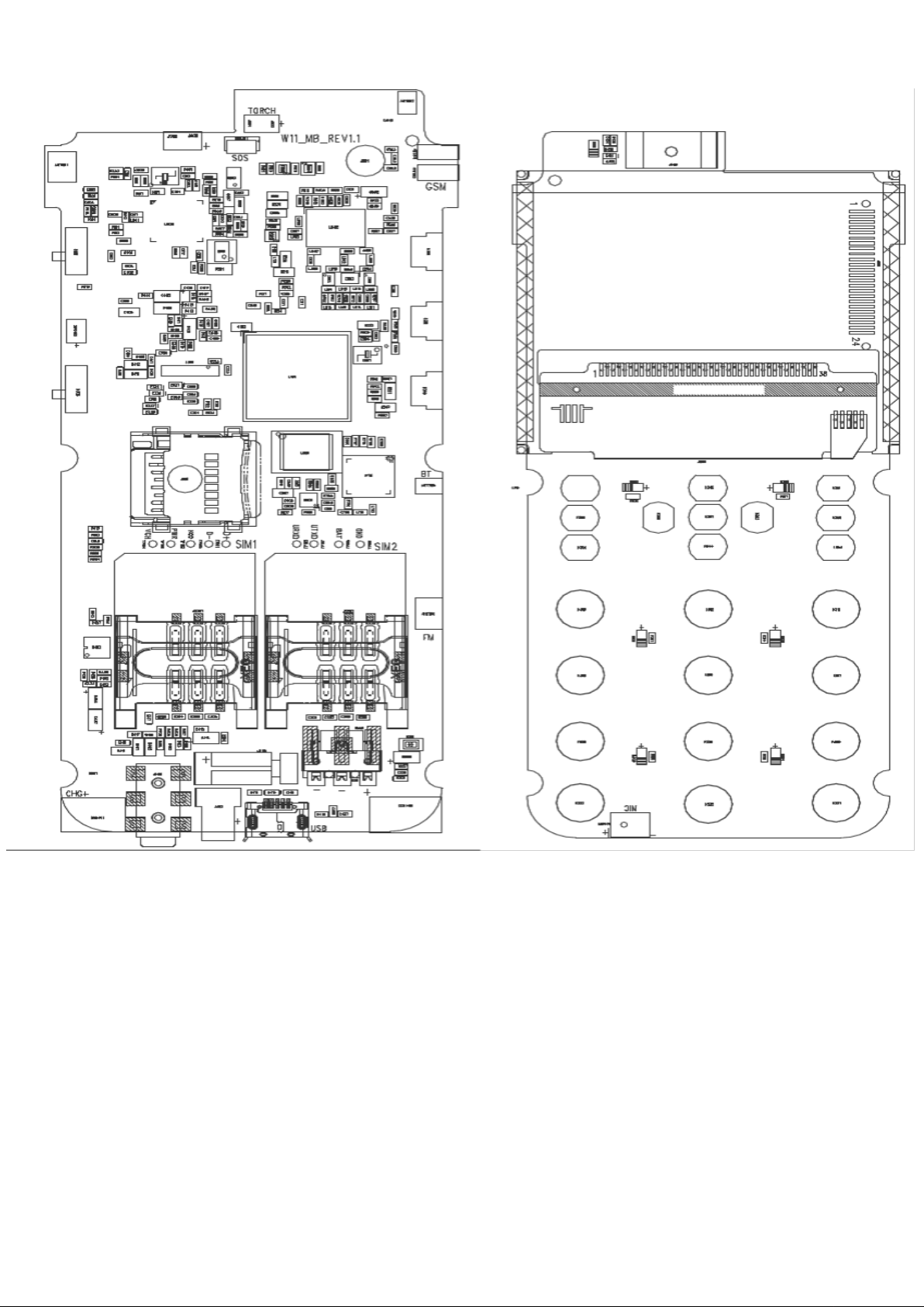
The main board placement
Chapter 3: Explanation of Schematic
Chapter 3: Explanation of Schematic
3.1 Principle of RF circuit
3.1.1 Principle of receiver circuit
3.1.1.1Rx signal flow chart:
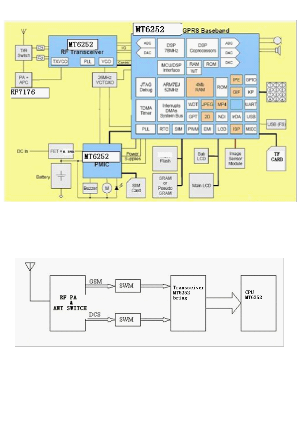
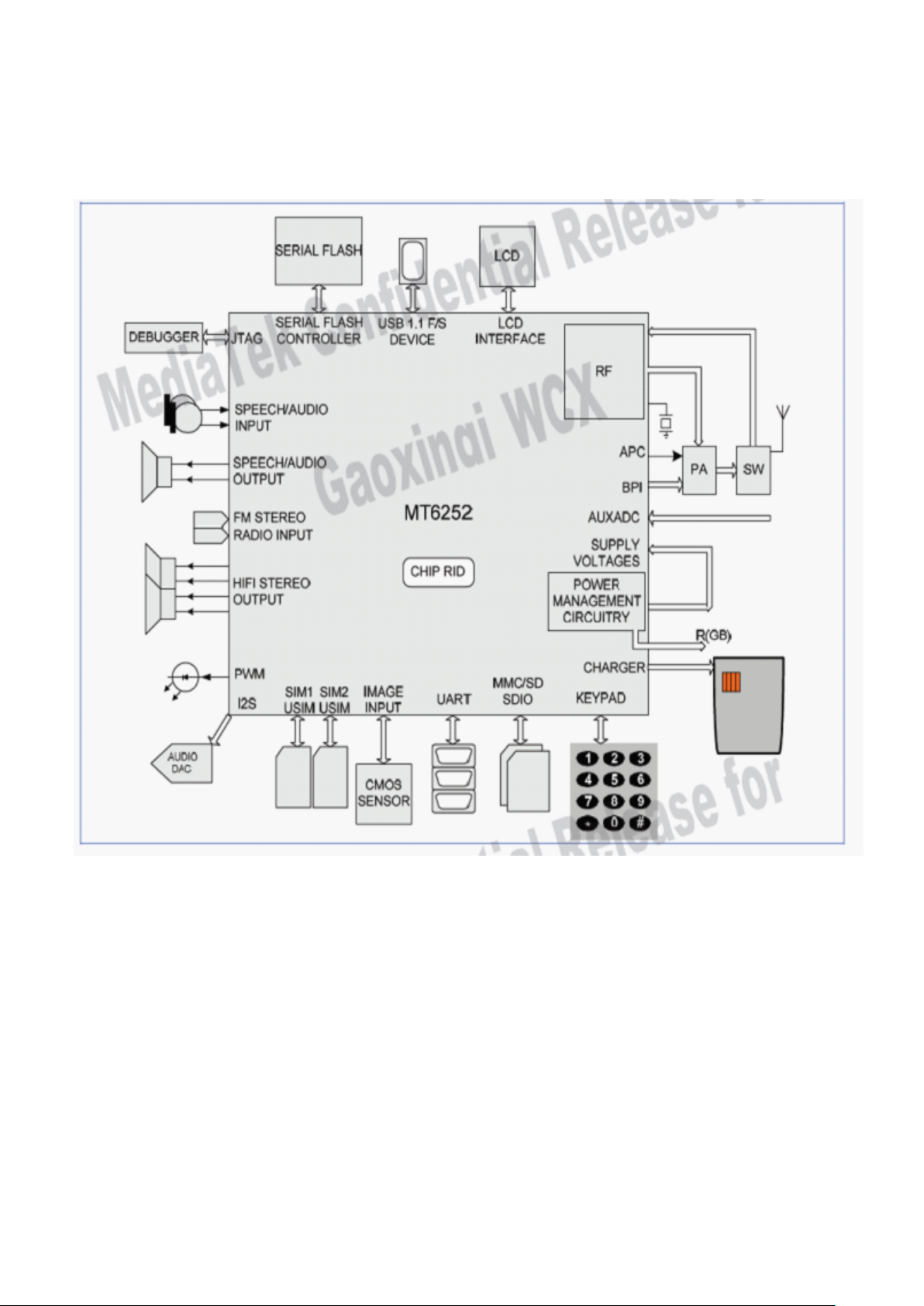
Picture 3.1 MT6252 principle picture
Picture 3.1.1 Receive signal flow frame
3.1.1.2 Main function of RF
RF part generally means the analog RF and IF process system ,including Antenna system、
TX path、RX path、Analog modem and Frequency Synthesizer
.
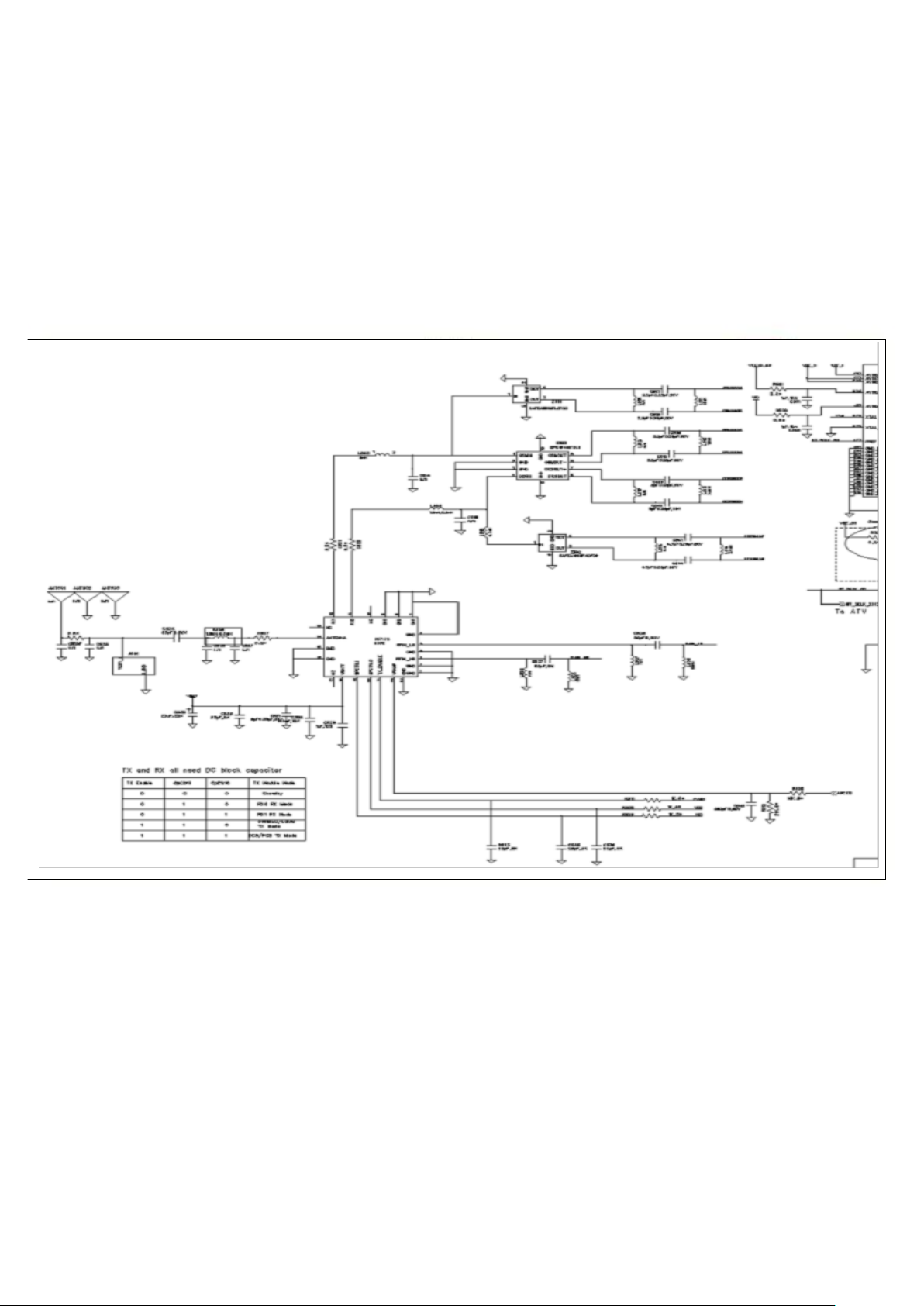
RF Circuit deals with the RX and TX of wireless signal, with responsibility for the bidirectional
Transmission of speech and data between the MS and BS through the air interface. In detail RX part
Accomplishes the AGC amplifying, mix and demodulation of RF weak signal received from BS, The
Final signal output from RX part is the analog baseband I/Q signal. The final RX I/Q will be sent to
Baseband Circuit for later disposal. On the other hand TX part deals with the signal modulation,
Up-conversion mix and power amplifying of analog I/Q signal received from baseband, generating
Burst which meets the GSM specification. And then the bursts are transmitted to Base station through
The antenna. The signal interface between RF Circuit and Baseband is analog baseband I/Q signal. The
Performance of RF Circuit can directly affects the signal transmission quality of the mobile phone!
The schematic of RF block for MTK GSM Dual-band RF solution is show below:
From the chart we can see that the RF part is mainly composed of a highly integrated CMOS
Transceiver chip (MT6253), some RX Saw filters, reference crystal oscillator, power amplifier,
Antenna switch module, antenna and the matching components between each other...
3.1.2 Direct Conversion Receiver
-Differential LNA
-Integrated Active RX Channel Select Filters
-Programmable Gain Baseband Amplifiers
-The receive path
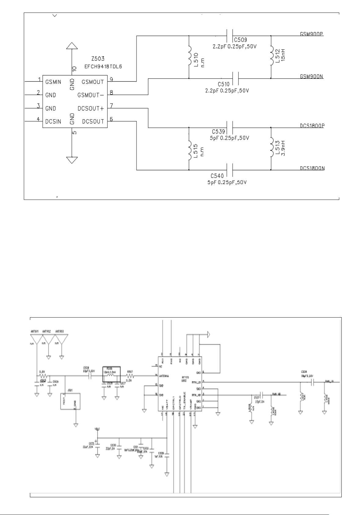
RX Saw filter Circuit
3.1.3 Translation Loop Direct VCO Modulator
-Integrated TX VCO and tank
-External TX filters eliminated
-Integrated Loop filter components
-Transmit Path
AD6548 uses only a single VCO source to derive the local oscillator signal for both the Feedback Down-
Converting Mixer and the Quadraturemodulator
TX PA: RF7176
TX PATH:
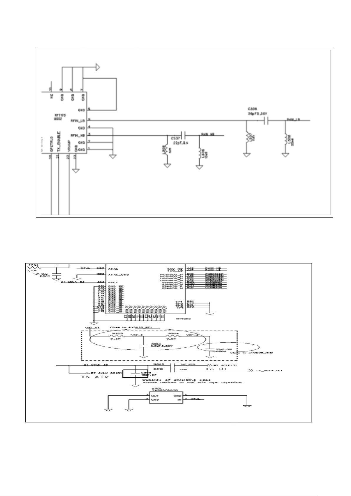
3.14 26MHz Clock:
-The entire system including VCO, tank, fractional N dividers, sigma delta compensation, charge pump and
loop filters are fully integrated.
-The only external component is the frequency reference.
26MHz Clock Reference circui
3.1.5 High performance multi band PLL system
-Fast Fractional-N Synthesizer
-Integrated Local Oscillator VCO
-Fully Integrated Loop filters
-Crystal Reference Oscillator & Tuning System
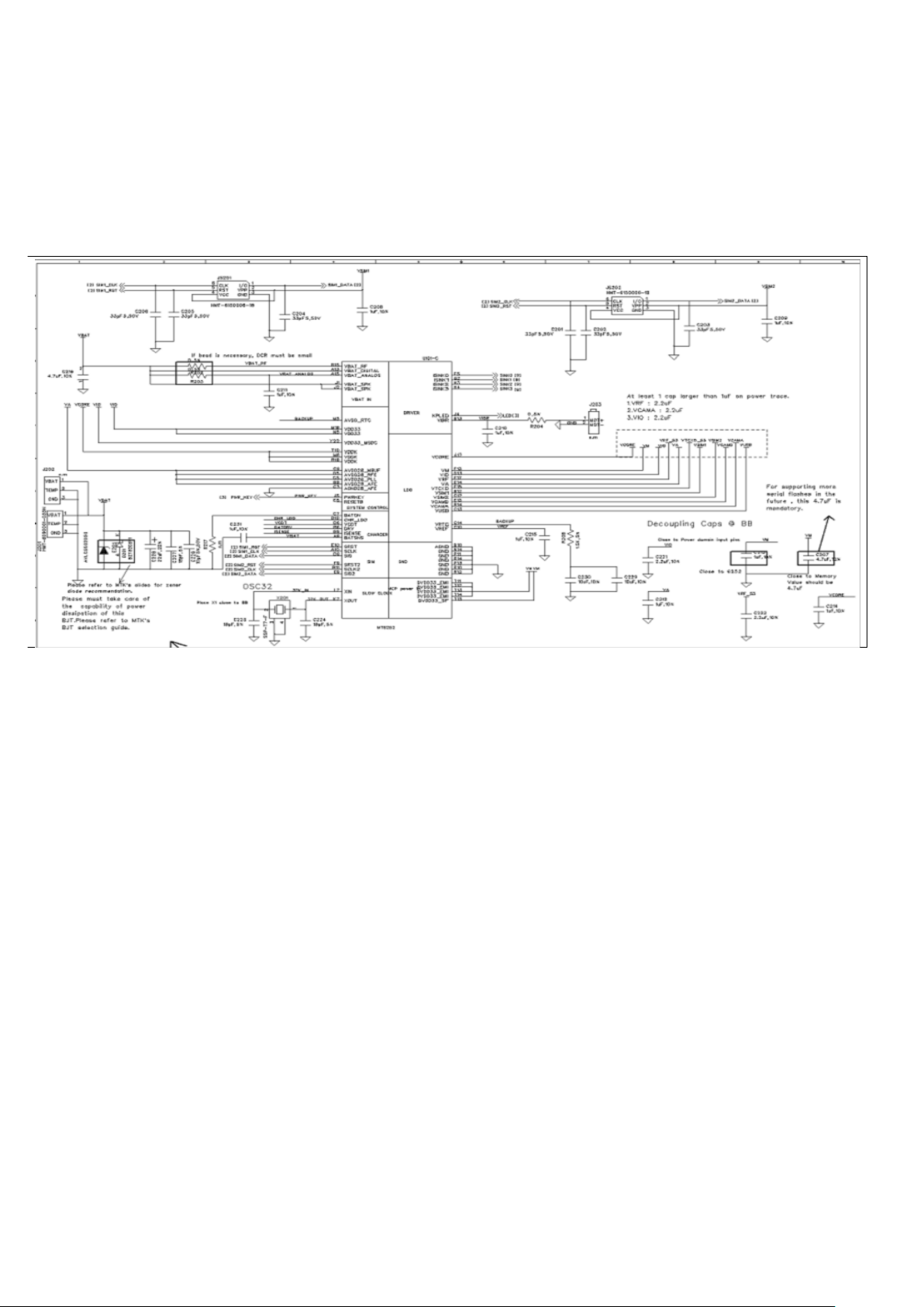
3.1.6 Power Management
-Integrated LDOsallow direct battery supply connection
3.1.7 Frequency ranges
The frequency ranges of the synthesizer for RX mode:
RX mode
E-GSM 900
DCS 1800
The frequency ranges of the synthesizer for TX mode
TX mode
EGSM900
DCS1800
925.2MHz ~ 959.8MHz
1805.2 MHz ~ 1879.8MHz
880.2MHz ~ 914.8MHz
1710.2 MHz ~ 1784.8MHz

MT62523.1.3 Function Block Diagram
3.2Principle of base band circuit
3.2.1 Whole introduction of base band circuit
3.2.2 Explanation of power circuit and in-and-out circuit
Power source is provided by MTK MT62 and periphery components, main function as below:
A.
B.
C.
D.
E.
F.
G.
H.
I.
J.
K.
I.
M.
2.8V-5.5V Input Range
Charger input up to 8V
Seven LDOs optimized for specific GSM Sub-systems
One LDO for RF transceiver
High operation efficiency and Low stand-by current
Li-Ion battery charge function
SIM Card interface
Two open-drain output switches to control the LED and vibrator
Three NMOS switches to control RGB LEDs
Thermal Overload Protection
Under Voltage Lock-out Protection
Over Voltage Protection
Power-on Reset and Start-up Timer
52
 Loading...