

Page 1

E195 Service Menu
Version number: V1.0
Contents
1 OVERVIEW E195..........................................................................................................................1
1.1 ABOUT E195 PHONE.................................................................................................................1
1.2 DISTRIBUTION OF THE MAINBOARD COMPONENTS ....................................................................3
2 RF....................................................................................................................................................5
2.1 RF OVERVIEW..........................................................................................................................5
2.2 TRANSMIT ................................................................................................................................5
2.3 RECEIVE ...................................................................................................................................6
2.4 COMMON RF MALFUNCTION....................................................................................................7
3 BASEBAND..................................................................................................................................18
3.1 BASEBAND OVERVIEW ...........................................................................................................18
3.2 LOGIC.....................................................................................................................................18
3.3 AUDIO FREQUENCY................................................................................................................18
3.4 BLUETOOTH WIFI CIRCUIT.....................................................................................................21
3.5 DUAL SIM – DUAL STANDBY SINGLE PHONE .........................................................................24
3.6 ATV CIRCUIT..........................................................................................................................24
3.7 BASEBAND COMMON MALFUNCTION ......................................................................................24
4 REFERENCE FOR MAINTENANCE......................................................................................29
4.1 NO SIGNAL .............................................................................................................................29
4.2 PHONE DOES NOT “POWER ON”...............................................................................................29
4.3 LCD TROUBLE........................................................................................................................29
4.4 SOUND TROUBLE ....................................................................................................................29
4.5 KEYBOARD MALFUNCTION .....................................................................................................29
4.6 CAMERA WITH FLOWERY/BLANK SCREEN...............................................................................29
Page 2

E195 Service Menu
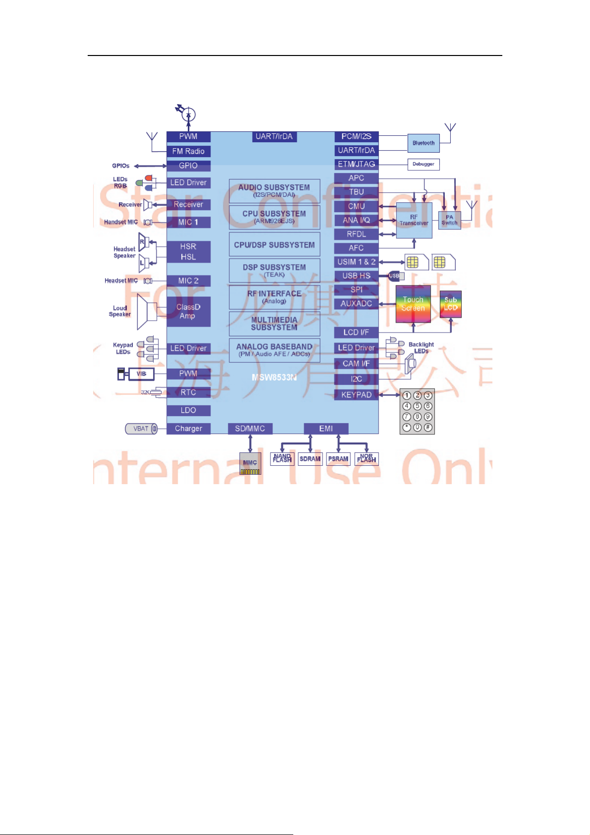
1 Overview E195
1.1 About E195 Phone
E195 mainboard is based on the MSTAR platform, which is supporting GSM/GPRS:
900/1800/850/1900MHz GPRS three-frequency communication. It is Dual SIM – Dual
Standby Single the mobile phone. The phone has the following feature:
1, Three specialties: 3.5 HVGA (resolution 320 * 480) LCM, 5M camera, ultrathin 10.9 MM
2, Dual SIM – Dual Standby Single PDA, compatible with three configurations: basic
configuration + WIFI + ATV
3, Support NOKIA specification device: BL- 5C battery, MICRO 5PIN interface
D104
RF7163 ASM
D301
H8ACS0PE0MBR-46
M-C
NAND+LPSDRAM
T-FLAHS-CART
D605
MSB7602
WIFI+BT
D1056
SI4210
TRANSCEIVER+PA
D201
MSW8533N
CPU
D608
ACRUX21
BT
LCM
摄像头
KEY
KEY_LED
RGB_LED
MOTR
B_LED
AUDIO
SENSOR
1
Page 3
E195 Service Menu
2
Page 4

E195 Service Menu
1.2 Distribution of the mainboard components
3
Page 5

E195 Service Menu
4
Page 6

E195 Service Menu
2 RF
2.1 RF Overview
RF part mainly consists of transceiver AERO4210HN (adopts program of near-zero IF
receiver, supporting the EGSM / DCS and 26M VCTCXO as the clock input, integrated
clock buffer, LO VCO and TX VCO and regulator, only need for external connections of
VBAT / AVDD.
GSM RF and BB interface diagram
Transceiver (AERO4210HN) with the RF modulation and demodulation functions contains
IF frequency synthesizer and VCO RF, which is part of the core component of the RF. PA
has a major role in amplification of modulation signal, and it must be controllable and the
speed should meet the GSM agreement.
Baseband Chip
2.2 Transmit
TX is composed of the modulation loop, power amplifier and antenna switch. PLL is
mainly in the internal AERO4210HN, I / Q signal first enters into the AERO4210HN. After
entering the PLL the signal is modulated to RF, and then it outputs from the chip to PA,
converts into electromagnetic energy through antenna by the antenna switch after
enlarged.
PA:
This part adopts voltage control to achieve and its role is to amplify the signal power in
accordance with the requirements. It is divided to different power levels through VRAMP
signal. The transmit signal of GSM is 5 to 19, power is from 3.2MW to 2W while DCS is 0
~ 15, power from 1MW ~ 1W. PA is time-sharing work controlled by TX-EN chip, the output
power of P A is controlled by VRAMP (APC) through the voltage. PA is intermittent work, by
the BS to achieve the choice of frequency bands.
5
Page 7

E195 Service Menu
匹配网
匹配网
路径
路径
频段选择信号
BB
AMS
Host RF Launch Principle Diagram
Transceiver
RF 发射输出
RF Launch output
2.3 Receive
Accessed from the antenna, GSM signal arrives at AERO4210HNN through the front end
SAW filter; and it converts to I/Q signal which modulated in 100 KHZ carrier. Then, it goes
through the band-pass, getting amplification (gain controllable), filtering, amplifier (gain
controlled); and mixes to baseband signal 4-road I/Q. Finally, it outputs to CPU for
processing after filtering. In diagram, SDATA, SCLK are I2C serial signals, responsible for
the communication work between MSW8533N and AERO4210HN; LE is MSW8533N
enable signal of AERO4210HN; RFVCOEN is enable signal which can generate
frequency mixing vibration signal VCO; VAFC is automatic frequency control signal of
crystal oscillator.
ANT
Coaxial Switch
同轴开关及
&Antenna
matching circuit
天线匹配电
PA
Transceiver
GSM TX
GSM TX Path
DCS TX Path
DCS TX
MT6129
IQ
MT6225
I2C
Band selection signals
6
Host RF Receive Principle Diagram
Page 8

E195 Service Menu
Check IQ si
g
p
p
2.4 Common RF Malfunction
2.4.1 Detection and Maintenance Flow Chart of MS Transmit
malfunction
(No transmit) Connect PC and cell
hone with maintenance of line, use the
Repair software making mobile phone
access to transmit state.
Y
Check antenna switch
or matching network
Y
pin of Transceiver,
whether there is IQ
si
nal?
gnal input
Y
Check RF signal output
pin, whether there is
any RF signal?
Y
VBAT, PA_EN,
BANDSW_DCS,
VAPC, are they OK?
N
Check CPU
N
Check Transceiver,
whether there is any
RF out
ut signal?
N
Check
Transceiver
External RC
Replace PA
N
Check CPU
Y
Replace
Transceiver
2.4.2 The maintenance process of Transmit malfunction
Use the Repair software and make mobile phone access to transmit state. Choose 62CH
in GSM band, POWER Level for 5, DCS for 700CH, POWER Level for 0. Then, first
observe whether the current rises, and use the spectrum analyzer and oscilloscope to
observe the signal given in the above-mentioned flow chart, the specific signal waveforms
shown as below:
7
Page 9

E195 Service Menu
IQ signal waveforms of transceiver in transmit state:
3.10 I/Q
RF interface spectrum analyzer is as follows:
GSM transmit signal
8
Page 10

E195 Service Menu
DCS transmit signal
PA-EN waveforms of PA in transmit state:
PA-EN
9
Page 11

E195 Service Menu
PA. BAND-SW waveforms:
PA.BAND-SW (GSM)
PA.BAND-SW (DCS)
10
Page 12

E195 Service Menu
PA Vramp waveforms:
Vramp (pcl5)
Vramp (pcl 19)
11
Page 13

E195 Service Menu
g
2.4.3 Detection and Maintenance Flow Chart of MS Receive
malfunction
No Receive
Open Repair Software to connect PC with mobile phone, make the
phone access to receiving state, adjust signal generator to
corresponding CH, and connect the signal line to phone’s RX_SW.
Check IQ signal output pin
Y
Check CPU
Y
of Transceiver, whether
there is IQ signal?
N
Check Transceiver input
pin, whether there is any
input signal?
N
Are Transceiver
SDATA、 SCLK 、
LE、RFVCOEN all
correct?
N
Whether PA signal
input pin has
received any
nal?
si
N
Check or replace
antenna switch and
matching circuit
Y
Check RX-filter
Check Transceiver
External RC components
Check CPU
N
Check the
correspondi
ng power
supply and
circuits of
26MHZ.
Y
Whether the voltage
Transceiver used is
normal? Is 26MHz
normal?
Y
Replace
Transceiver
2.4.4 The maintenance process of Receive malfunction
Maintenance process of NO Receive: Use Repair software to make mobile phone access
to pure receive state → Choose 62CH, Rx Mode CH62=94 7.4MHZ, Input power:-60dbm
in GSM frequency bands → Choose 698CH, Rx Mode CH698=1842.4MHZ, Input
power:-60dbm in DCS frequency bands → Adjust signal generator to corresponding CH,
connect the signal line to Cable of RF → Measure the related key signal by using
Spectrum analyzer and Oscilloscope → Measure the signal output pin of Transceiver,
whether there is any correct IQ signal output to CPU → Y: Check CPU (MSW8533N) / N:
12
Page 14

E195 Service Menu
Check Transceiver input pin, whether there is any corresponding CH input signal (Y:
Check whether Transceiver has correctly controlled the signal → Check whether the
voltage supply is normal → if normal, Transceiver can be judged of damaged / N: Check
PA and the paths ahead ). Signal waveforms refer to the following:
Output signal of Signal generator (Input):
GSM CH62 channel receives the signal
13
Page 15

E195 Service Menu
DCS CH 698 channel receives the signal
IQ signal output pin of Transceiver the state of receiving IQ signal:
Test should have 2.8v voltage. The signal Transceiver received from CPU used to access
the internal register of Transceiver. The corresponding waveform is as follows:
14
Page 16

E195 Service Menu
3W(SDATA)
3W(SCLK)
15
Page 17

E195 Service Menu
3W(SCLK)
26M clock (can be measured by using the AC Coupling)
The RFCRTLCLK (automatic frequency control) from CPU to the crystal oscillator makes
26M crystal oscillator output accurate 26MHZ to Transceiver.
26M outputs to CPU
Crystal oscillator 26M input
16
Page 18

E195 Service Menu
VAFC
TCXO output(26MHZ)
17
Page 19

E195 Service Menu
3 Baseband
3.1 Baseband Overview
E195 Baseband mainly consists of CPUMSW8533N. MSW8533N baseband, the core
device of the mainboard, is responsible for the normal work among various parts of
mainboard, such as voice processing, image processing and MS communications.
Digital baseband MSW8533N contains 2-bit ARM7E kernel, 284Kbyte SRAM.
MSW8533N is enhanced GSM processor, in the internal integration, including channel
codec, interleaving/solution intertwined, and the encryption/decryption, channel codec
subsystem; including ARM7EJS and peripheral interface circuit, control processor
subsystem. Its external has 26 roots address line, 16 data line, eight chip selection lines,
provide 6 external center fracture port; 26 M / 52 M operating clock.
Analog baseband contains MSW8533N analog baseband chip, audio and baseband
codec. Three major functional blocks integrated internal: Audio codec including Voice
input / Output channel, Buzzer output; Baseband codec including Differential I, Q input /
output, GMSK modulation and A / D, D / A; Auxiliary parts including AFC DAC, RAMP
DAC, AGC DAC and a seven-channel A / D. And WATCHDOG interface is set internal to
enhance the stability of the system.
3.2 Logic
Logic part is composed of MTK base-band management chip MSW8533N, Power
management chip and NOR Flash.
MSW8533N:CPU
NOR Flash: H8ACS0PE0MBR-46M-C
3.3 Audio Frequency
Because MSW8533N inside integrates the audio processing, which makes the
performance of sound quality more conspicuous pleasing.
3.3.1 Speaker loop
Relative to the AUDIO CODEC, Speaker loop is simpler, only a PA and SPEKER. When
maintaining, pay attention to the signal waveform of PA input and output end.
18
Page 20

E195 Service Menu
3.3.2 MIC loop
Check basic bias voltage signal of MICBIASP and MICBIASN and the language signal of
MIC itself when the MIC is good but no response of LOOP MIC in test.
19
Page 21

E195 Service Menu
3.3.3 Earphone loop
Earphone loop includes headset speaker and MIC two-road signal. Check the circuit
access situation when there is something abnormal (such as: no sound in headset
speaker, MIC invalid, etc.) after inserting the earphone while the headset accessories are
good.
20
Page 22

E195 Service Menu
3.4 Bluetooth WIFI circuit
This phone hardware design, is compatible with two bluetooth project, 1: Through the
WIFI + BT two-in-one chip, put WIFI and Bluetooth together to deal with. 2: Use Bluetooth
chip alone, only keep BT function.
a/power part:
21
Page 23

E195 Service Menu
b/WIFI/BT receiving circuit
c/WIFI launch part
d/WIFI + BT chip
22
Page 24

E195 Service Menu
p
RF output
clock input
difference
RF antenna
in
ut
Power
control
single
e/single Bbluetooth chip circuits
Bluetooth
antenna
single
power part
Bluetooth clock
Bluetooth control
Bluetooth Chip
Selection
Bluetooth
data
23
Page 25

E195 Service Menu
3.5 Dual SIM – Dual Standby Single Phone
Dual SIM – Dual standby single phone is based on the GSM agreement, in standby mode,
communicate between mobile phones and base station with shaking hands. Because this
communication has the time gap, so we can switch two SIM to shake hands and performs
a set of system of double user SIM standby effect through the high speed. But when one
is calling, the other is forced to disconnect. After finishing the call, it will return to the dual
SIM – dual standby status.
3.6 ATV circuit
The phone supports ATV function.
3.7 Baseband common malfunction
3.7.1 OR Flash programming does not download
Data lines used for downloading software: VBA T, TX, RX, GND, CHARGE. It is mostly due
to the false solder and wire bonding. First check whether the serial port of PC and cell
phone is unrestricted, if not, it is caused by being lack of devices or empty solder of power
manager, USB-con and peripheral resistance. Measure the TX, RX signals by using
AC-coupled oscilloscope to track the signal flow, if a certain period circuit of no signal it
may be AC short circuit to ground, or is caused by a short circuit and open circuit. On
checking the malfunctions, first should carefully observed the welding of these devices
with a magnifying glass, then plug in the download line to observe whether the current is
normal, there is short-circuit to ground of VCHG or VBAT if the current is large, at this time
cut off power supply as soon as possible, and then find the short-circuit point. It may be
the abnormal output power supply of a certain circuit that the current is larger than normal
(about 30 mA) but not particularly large, at this time should check whethe the valgate of
VCORE (1.8V), VDD (2.8V), VADD (2.8 V), VTCXO (2.8V), VRTC (1.5V), VMEM (2.8V) is
noamal, if not, bad welding can be detected. Focus on checking the welding of PMU and
USB-CON if there is a little or no current. Unplug and re-plug the download line to see if it
is caused by poor contact; It can test that whether the output of 26MHz clock signal to the
CPU is normal by using oscilloscope.
3.7.2 Detection and Maintenance Flow Chart of No download
malfunction
24
Page 26

E195 Service Menu
N
d
Not download
Eliminate any reasons
for not download
except the cell phone.
Check whether the 8pin
connector USB-CON is
false soldered or
damaged.
Yes
NO
Check whether it is the problems of
allocation of procedure, download cable,
power supply, software, PC phone.
Check whether the serial port of PC and
cell phone is unrestricted.
NO
Check USB-con
peripheral resistance
Connect the download line and observe the
ammeter whether the current is high
(normal current is generally about 30mA).
A little or no current
Check whether the voltage supply of CPU power
manager, PMU and LDO is normal, whether there is
any power supply open circuit.
NO
Yes
Quickly disconnect the
connection, and touch the chip
Yes
gently to see if it is hot, if not,
focus on measuring the
short-circuit point by using
multimeter.
ormal current but no downloa
Check VCORE、VDD、 VADD 、VTCXO、
VRTC、VMEM、measure the clock signals of
26MHZ、32KHZ.
Check whether CUP and NORFLASH is OK,
LDO is normal?
25
Page 27

E195 Service Menu
3.7.3 LCM circuit analysis
LCD control
signal
LCD data
signal
The signal waveform
Chip select signals CS:
26
Page 28

E195 Service Menu
Screen reset signal LRST:
Screen Write signal LWR:
27
Page 29

E195 Service Menu
About the screen, first find the problem whether is mainboard or screen by adopting
replacement method, then focus on checking the LCM-CON welding.
28
Page 30

E195 Service Menu
4 Reference for maintenance
4.1 No Signal
The common processors: Transceiver, PA.
4.2 Phone does not “power on”
The phone can not power on is usually caused by false welding. Firstly, check the signal
integrity of 26MHZz, 32.768KHz as well as the continuity of signal path. Then, check the
integrity of core voltage and path. Generally, CPU will less be damaged, and it is due to
smaller current but normal voltage, at this time Replacement method should be adopted,
and try to do welding, re-welding.
4.3 LCD trouble
Re-welding display interface and nearby resistance row, as if it is still abnormal, check the
DSP components whether it is of short circuit.
4.4 Sound trouble
E195 audio processes in internal CPU, focus on checking the Audio-PA on the issue of
free or miscellaneous ring tones. Low ring for checking its solder joints (very small, and
easy to cause problems during SMT). Try more times for re-welding and replacement.
4.5 Keyboard malfunction
In most cases there is something wrong with the linking of single button with circuitry if
only this button does not work. Focus on checking the resistance row near the display or
whether CPU is short circuit if group buttons do not work.
4.6 Camera with flowery/blank screen
First check the Interface whether there is any false solder, and check whether the
peripheral components are missing.
Note: The waveforms may be different according to the settings and different devices in
maintaining.
29
 Loading...