

Page 1

Fly E175 Wi-Fi
Repair Service Manual
Release Date : 2011/6/10
- 1 -
Page 2

table of content
1. General features and specifications.......................................................................................... 3
2. Decomposition diagram.............................................................................................................8
3. Fly E175 Wi-Fi Circuit.................................................................................................................9
4. Components address confirmation.............................................................................................39
5. Baseband Trouble.......................................................................................................................41
6. RF Trouble..................................................................................................................................62
7. Fly E175 Wi-Fi disassembly and assembly..................................................................................66
8. Fly E175 Wi-Fi SELF TEST..........................................................................................................74
9. Fly E175 Wi-Fi upgrading ROM procedure...................................................................................75
- 2 -
Page 3

1. General features and specifications
Model name / Spec
E175 Wi-Fi
General
Standard GSM900/DCS1800
Size (H x W x T) 112*56.5*13
Weight (gramms) 102g
Battery 1000 mAh, Li-Ion
Talktime (h) 4
Stand by (h) 300
Platform (MTK chipset) MTK6236
Design
Form factor Full touch
Antenna built in
Smartphone
Processor
ОS
Display
Resolution (pixels) 240*400
Description TFT 262K colors / 3.2"
Touch screen Resistive
External display no
Size
Description
Camera yes
Image
- 3 -
Page 4

Resolution (Mpx) 3.2 MP(extrapolated by SW)
Video recording (pix.) QVGA (320x240)
Flash yes
Digital zoom yes
Modes Normal,continuous shot,panorama,add frame
Effects
normal,grayscale,sepia,sepia green,sepia blue,color
invert
Web-camera yes
Flash-light (torch) yes
Audio player yes
Formats mp3, aac, amr, wav, mid
Equalizer
(normal, bass, dance, classic, treble, party, pop, rock)
yes
Manual eualizer setup no
Bitrate -
Work time (hours) up to 9
Playlists yes
A-B repeating function yes
Video player yes
Format MP4, 3GP
Sound coding AMR, AAC
FM Radio yes
Availability yes
FM schedule recording no
Entertainment
Games yes
Photoeditor no
- 4 -
Page 5

Dictophone no
TV-out no
E-book yes
Graphic editor no
Background sound no
Java yes
MIDP 2.0
CLDC 1.1
Available memory 300Kb
Cash 100Kb
Preinstalled JAVA application
Bluetooth yes
Version 2.1
A2DP yes
DUN no
HFP yes
GAVDP no
AVRCP yes
FTP yes
OPP yes
SPP yes
HID yes
SAP yes
FAX no
Obex Imaging Responder
IRDA no
Availability no
Mobile internet
E-mail client yes
WAP 2.0
GPRS yes
GPRS class class 12
GPRS-modem no
OTA support no
Memory
Built-in (Mb) 1Gb+512Mb
Memory card support microSDHC (up to 8Gb)
USB storage yes
- 5 -
Page 6

Organizer
Calendar yes
Alarm clock yes
To Do List yes
Reminder yes
Notes yes
Auto on/off yes
World time yes
Calculator yes
Currency Converter yes
Unit converter yes
Stop-watch yes
Тimer no
Biorhythm no
Call signals
Melodies
supports download from web or from PC
Polyphony 64-tones polyphony
Format
MID,WAV,AMR,AAC,MP3
Vibro yes
Melody editor no
Phone book
Memory 1000 cells
Entry fields
home, company name, E-mail, office, fax, birthday,
picture, video, ringtone, group
Photo ID yes
Melody ID yes
Editing on PC no
Synchronization with PC no
Messages
SMS yes
EMS yes
MMS yes
Other functions
Autodial yes
Additional information 3.5mm jack, Dual-SIM support etc.
- 6 -
Page 7

Packing
Memory card no
Battery yes,1pcs
Charger yes
Desktop charger no
USB cable yes
Earphones yes
CD no
Manual yes
TV out cable no
Warranty card (new black) yes
WAP advertising card yes
Certificate information card yes
Other
- 7 -
Page 8

2. Decomposition diagram
- 8 -
Page 9

3. Fly E175 Wi-Fi Circuit
3.1 MT6236 System Overview
3. Fly E175 Wi-Fi Circuit
- 9 -
Page 10
- 10 -
Page 11

- 11 -
Page 12

- 12 -
Page 13

- 13 -
Page 14

Pin Description
- 14 -
Page 15

- 15 -
Page 16

- 16 -
Page 17

- 17 -
Page 18

- 18 -
Page 19

- 19 -
Page 20

3.2 RF transceiver
MT6140 RF transceiver
MT6140 is a highly integrated RF transceiver IC for Global Systems for
Mobile communication (GSM850, GSM900), Digital Cellular communication
Systems (DCS1800), and Personal Communication Services (PCS1900) quad
band cellular systems. It includes four LNA's, two RF quadrature mixers, a
channel filter, a programmable gain amplifier for the receiver, two high
precision I/Q modulators for the quad band transmitter, on-chip regulators, and
a fully programmable sigma-delta fractional-N synthesizer with an on-chip
LC-tank VCO. The MT6140 includes control circuits to implement different
operating modes. The device is housed in a 40-pin QFN SMD package with a
paddle for additional grounding.
- 20 -
Page 21

- 21 -
Page 22

- 22 -
Page 23

SKY 77546 Rx-Tx Module
The SKY77546 is designed for dual-band cellular handsets comprising GSM900 and DCS1800
applications and offers a complete Transmit VCO-to-Antenna and Antenna-to-Receive SAW filter solution that
supports Class 12 General Packet Radio Service (GPRS) multi- slot operation and EDGE operation.
The module consists of a GSM900 PA block, a DCS1800 PA block, a Power Amplifier Control (PAC) block,
impedance-matching circuitry for 50Ω input and output impedances, Tx harmonics filtering, high linearity and
low insertion loss RF switches. A custom CMOS integrated circuit provides the internal PAC function, external
interface circuitry, and decoder circuitry to control the RF switches. The integrated PAC function provides
envelope amplitude control by reducing sensitivity to input drive, temperature, power supply, and process
variations. The output of each PA block and the outputs to the two receive pads are connected to the antenna
pad through a diplexer and SP2T switch.
Band selection (BS) and Tx and Rx RF signal flows are controlled five external control pads: BS selects
GSM or DCS modes; Tx_EN selects Rx or Tx mode of the respective RF switch (Tx = logic 1); SW_EN provides
improved isolation for control timing flexibility to meet the required time mask; MODE configures the amplifier for
GMSK operation (MODE = 0) or linear EDGE operation (MODE = 1). Proper logic timing and Analog Power
Control (APC) allows high isolation between antenna and Tx-VCO while VCO is tuned prior to the transmit burst.
The integrated PAC function provides envelope amplitude control and bias optimization for each operational
mode, reducing sensitivity to input drive, temperature, power supply, and process variation. Standby mode
provides a low-current consumption state. Low leakage current (6.5 A, typical) of the dual PA module
maximizes handset standby time.
- 23 -
Page 24

- 24 -
Page 25

3.3 S200 WiFi SIP module
Description
AcSiP Technology Corp. introduces a low-cost and low-power consumption WiFi SIP module. The
module is targeted to mobile devices including smart phone, PDA, WiFi phone, DSC, DVC which need
small WiFi module. The highly integrated module allows the usage of web browsing, VoIP application.
The wireless SiP module support IEEE 802.11b/g standard and it can provide up to 54Mbps for IEEE
802.11g, 11Mbps for 802.11b to connect your wireless LAN.
Key Features
Small footprint : 9.0 mm X 9.0 mm X 1.4 mm
Host interface : SDIO / eHPI16 / eHPI8
Support Orthogonal Frequency Division Multiplexing(OFDM), Complementary Code
Keying(CCK),
and Direct Sequence Spread Spectrum(DSSS) to provide a variety of data rates
Support ad-hoc and infrastructure modes
IEEE 802.11g(OFDM 54Mbps) and IEEE 802.11b(DSSS 11Mbps)
Support Bluetooth co-existence
Support low power consumption sleep mode via 32 kHz clock
IEEE 802.11i(AES, TKIP, 802.1X) for advanced security
IEEE 802.11e QoS support for multimedia applications
Wakeup by specific packet(pattern search)
64/128-bit Wired Equivalent Privacy (WEP)
Shared clock, EEPROM, and full RF front ends integrated for WiFi
40MHz crystal embedded
RoHS compliant / Lead free
OS support WinCE/Win Mobile (V6.0/V6.1) and Linux
Specification
- 25 -
Page 26

- 26 -
Page 27

RF circuit
- 27 -
Page 28

MT6236-Baseband circuit
- 28 -
Page 29

- 29 -
Page 30

Flash Memory circuit
- 30 -
Page 31

MT6236-PMU circuit
MT6236-IMPUT circuit
- 31 -
Page 32

Charging circuit
Vibrator circuit
- 32 -
Page 33

Handset Mic circuit
Handset REC circuit
- 33 -
Page 34

Earphone Mic circuit
Loud Speakers circuit
- 34 -
Page 35

LCM circuit
Camera circuit
- 35 -
Page 36

T-Card circuit
USB I/O circuit
- 36 -
Page 37

SIM Card circuit
BT circuit
- 37 -
Page 38

FM circuit
Wi-Fi circuit
- 38 -
Page 39

4. Components Address Confirmation
- 39 -
Page 40

- 40 -
Page 41

5 Baseband Trouble
5.1Preparatory work for repair
5.2 Flash programming does not download
Analysis Process:
- 41 -
Page 42

Not Download
NO
or VBAT
short circuit
and GND
No wave output
whether there is short
Download is mainly communications
Current>300mA
Slight large than normal
voltage (UTX,URX
VCHG
whether
VCORE( 1.2V) 、
AVDD( 2.8V ) 、
VDD( 2.8V ) 、
VTCXO( 2.8V) 、
VMEM(1.8V) 、
VRF(2.8V)
Check voltage
whetheris normal,
reverse Resistance
whether is normal,
circuit
between the CPU and FLASH,
including the line of control, address
lines and data lines. If check external
circuit no problem, CPU and
FLASH welding no problem,the final
issue may itself access to the
PCB,there are problems -
removed the CPU and FLASH, Trace
of the on-off
5.3 Phone does not "power on"
Check
current
YES
Check test point
is 2.8V)
YES
YES
Check 26MHz
YES
Little or no current
Check the
corresponding
signals in the
circuit-off
First check U200 whether
there is VCCRF output;
secondly,check welding of
the OSC100
Check VBAT
, VCHG
voltage
whether is
normal, If
there is no
voltage,
check welding
of the system
I/O
Power on principle of phone: When the power supply is connected with the phone, through internal
switching circuit in the boot it will form a trigger High-level, when press boot button long enough, the
boot high-level change to low-level because of connecting with GND, and the signal reaches PMU block,
PMU will activate the internal voltage regulator and output stable voltage, as a logical part of the core
CPU will gain power supply.
We know phone boot in three necessary conditions: Power Supply, clock and reset. Now power
- 42 -
Page 43

supply has been provided, then Crystal will produce 26 MHz clock signal, on the one hand it will be
signal output
the CPU and
FLASH
NO
taken as a RF reference clock, on the other hand, it will be sent to logic to the clock signal. After the
clock signal reaches the microprocessor, the memory before need be cleared, therefore PMU will send
reset signal to it for initialization. After the initialization is finished, it outputs control commands to
memory, then memory will change to permit state, and then through address line to look up where boot
program is, after finding the boot program it will be sent to CPU internal DSP circuit through data lines.
After the successful operation, the CPU output signal to PMU, the power supply will continuously output
voltage to complete booting.
After phone powers on, the CPU calls RF parameters from flash, through radio BCCH to receive
the signal intensity in the area, if your phone has a SIM card or UIM cards, Mobile phone will send the
information in SIM card to the BS, and receives information from the BS, thus achieve network
connections.
After being connected with networks, mobile phones will be in a idle mode, but also mobile phones
through SACCH periodically exchange some information with base stations, such as signal strength
and frequency synchronization, receiving level, and receiving quality
Analysis Process:
Download ok, but
No power on
YES
Re-download
NO
Measure whether
there is 32KHz
YES
Check communications
between the CPU and
YES
END
Software problem
NO
Measure VRTC whether there is
2.8V voltage output,or else
re-welding or change X200
Communications between the CPU and
FLASH,including the line of control,
address lines and data lines.If check
external circuit no problem, CPU and
FLASH welding no problem,the final
issue may itself access to the PCB,there
are problems - removed
FLASH, Trace of the on-off
- 43 -
Page 44

5.4
Sound trouble
software
Analysis Process:
Sound trouble :
Ringtone/MP3
Check SPK
Re-download
Check welding of
U400 (Audio PA)
NO
Re-welding or change
U200(CPU)
END
Reference circuit as follows:
YES
Re-welding or change SPK
NO
Check welding of the SPK
peripheral circuits
NO
YES
- 44 -
Page 45

5.5 Can not charge up
software
Charging principle introduce:
When the charger inserted, Charge for the PMU module provides voltage Charge,As long as the
PMU of the BATDET pin grounding can start charging module,at this time will result in a charge
interrupt signal to CPU,to inform the CPU has entered a state-of-charge now. PMIC will then generate
an interrupt to the CPU,CPU Started as follows module:
1. ADC sampling, mainly collected Vchrg, Vbat and the output from the MOSFET drain voltage Vbat
and the adoption of Vd (MOSFET drain) and Rsense value, you can calculate the charge current!
That is, we *#94683538# in ADC display options Icharg, Vchrg, Vbat, and other information!
2. Send a message to the MMI layer, it shows that state-of-charge and some sample data
3. Testing battery voltage whether more than protection voltage and battery voltage connection is
correct,If there is any problem you can cut off the charging circuit through CHRCTRL!
Analysis Process:
Can not charge up
Re-download
Measure VCHG
whether is 5V
YES
YES
NO
Check welding of CON508 and
connect of the charger
Check the battery voltage
is below 4.2 v
NO
Battery power saturation
Check welding of
MOSFET(U310 U301)
YES
NO
Re-welding or change U310 and U200
END
Reference circuit as follows:
- 45 -
Page 46

5.6 LCD trouble
LCD backlight driver circuit:
- 46 -
Page 47

No Display
No Blacklight
No No
No
No
No
Analysis Process:
CheckU505
LCD Trouble
Check EMI part
welding of the U500 U501
U502 U503 U504
Re-welding or change
Check FPC
Check FPC
welding
welding
Yes
Check LCD
module
Re-welding or change
Change LCD module
Yes
Re-download
software
END
Re-welding or change CPU
- 47 -
Page 48

No
Value whether
is 1K
No
5.7 Keyboard not function
Analysis Process:
KEY not function
,R206,R208,R209,R210,R21
1,R221,R222,
Re-download
5.8 Microphone trouble
Reference circuit as follows:
Yes
Check part
Yes
software
Yes
END
Whether insufficient Solder
Re-welding or change CPU
- 48 -
Page 49

No
No
No
Analysis Process:
MIC not function
Yes
Check MIC
Yes
Check mic external
circuit
Yes
Re-download
software
Yes
END
5.9 Earphone part trouble
1、Bias voltage:MICBIASP(2.2V);
1.Re-welding or change
2.Check PCB mic pad whether short-circuit
1 .Check whether there is part miss
2. Check whether there is part unconnected solder
3. Measure signal in the circuit show
Re-welding or change CPU
2、Headphone detection signal: HEAD_DET: When insert earphone, due to XMP3_R
connection with speaker,HEAD_DET signal grounding,Trigger interrupt to the CPU,Will show "Insert
headphone";
3、Headset to hang up signal detection:AUX_IN5_EARPHONE:This signal is used to detect whether the
headphones of the hang up button Press,when the headset hang up button is pressed, XMICP signal
will be shorted, AUX_IN5_EARPHONEwill be shorted at one time;
- 49 -
Page 50

5.10 USB transmit trouble
Reference circuit as follows:
USB Circuit Working Principle:
1、Phone through the USB data line and computer connection, charge signal trigger phone auto power on
2、External power supply (USB_PWR)connect to mobile phone, USB ADC signal voltage will be low to
the high jump, trigger bring interrupted signal;
3、CPU implementation USB interrupt;
4、CPU and computer through the USB interface for data transfer;
- 50 -
Page 51

No
2.Check headset whether inserted in the
end
N
3.Change
CON508
No
Analysis Process:
USB transmit trouble
YES
Check USB
connect
Yes
Check USB jack
Yes
Check PC driver
whether correct install
YES
END
1.To confirm the correct use of usb cable line
o
1.Check CON508 PIN whether un-connect
solder
2.Check CON508 whether internal damage
Re-welding or change CPU
- 51 -
Page 52

No vibration
whether
No
No
5.11 Vibrator trouble
Reference circuit as follows:
Analysis Process:
Open vib ,measure
VIBRATOR
there is low level
Re-download
software
END
Yes
Yes
Re-welding or change Vibrator
Re-welding or change CPU
- 52 -
Page 53

5.12 Receiver does not work
there is a wave
output
No No
external circuit
No
Reference circuit as follows:
Analysis Process:
Receiver Trouble
Engineer model, open
receiver , scilloscope
measurements whether
Yes
Yes
1 Check receiver whether the good contacts with
the PAD
2. Clean PCB PAD
3. Change receiver
Check receiver
Re-download
software
END
5.13 Camera trouble
Reference circuit as follows:
Yes
Check red mark part in the circuit show
Re-welding or change CPU
- 53 -
Page 54

Analysis Process:
sensor
No
FPCB
No
sensor
No
No
Camera trouble
Yes
Check the
condition of the
Camera module, LDO
Yes
Check the soldering
Condition of
CON503& Tail
Yes
Check camera
Check camera
Yes
Re-download
software
END
Check the solder condition of U706
Change new camera sensor
Re-welding or change CPU
Re-welding or replace it
- 54 -
Page 55

5.14 Bluetooth has not function
No
No
No
Reference circuit as follows:
Analysis Process:
BT trouble
Check BT headphones
Yes
Check BT external circuit
Yes
Check the soldering
condition of U700
Re-download
Yes
software
Yes
END
1.Power support :VBT
2.Check clock:26M
Re-welding or replace it
Re-welding or change CPU
- 55 -
Page 56

5.15 Motion sensor trouble
Reference circuit as follows:
- 56 -
Page 57

No
No
No
Analysis Process:
Motion sensor
trouble
open motion sensor function
Measure VDD whether is 2.8v
Yes
Measure
GPIO61_SENSOR_SDA
GPIO60_SENSOR_SCL
whether is 2.8v
Yes
Re-download
software
END
Re-welding or change U200
Re-welding or change U200
Re-welding or change CPU
- 57 -
Page 58

5.16 FM trouble
Reference circuit as follows:
- 58 -
Page 59

No
No
No
No
Analysis Process:
FM trouble
Yes
Check headphones
Yes
Check FM external
circuit
Yes
Check the soldering
condition of U702
Yes
Re-download
software
END
Re-welding or change CPU
1.Check headphones whether inserted in the end
2.Check headphones jack whether unconnected solder
1.Power support :VDD
2.Check RTC:32.768KHz
3.Check external whether there is missing and unconnected solder
Re-welding or replace it
- 59 -
Page 60

5.17 Phone can not access SIM card
No
No
Reference circuit as follow
Analysis Process:
SIM trouble
Check SIM card
base
Yes
Yes
Re-download
software
END
Whether unconnected solder
SIM card whether true insert
Re-welding or change CPU
- 60 -
Page 61

5.18 TF card trouble
No
No
Reference circuit as follow
Analysis Process:
Check TF card
base
Can not access
TF card
Yes
Yes
Re-download
software
END
Re-welding or replace it
Re-welding or change CPU
- 61 -
Page 62

6 RF Trouble
6.1 Principle of operation
Signal TX processes:
Acquisition voice - Amplification - ADC - filter - Speech Code - Complect - encryption - Channel
Equalization - GMSK modulation -- ( into RF part) IQ modulation (IQ modulator) - filter -- Frequency
phase (phase frequency) - filter - TX_VCO mixer (Mixer Mixer) - power amplifier (PA) - duplex --
Antenna matching circuit - antenna TX
Signal RX process:
Antenna RX - antenna matching circuit - duplex Filter - SAW filter - LAN - RX_VCO mixer -
Amplification - filter - IQ demodulation (IQ Modulator) - GMSK demodulator - Channel Equalization -
decrypt - Cutting Complect - voice codec's - filter -- DAC - Amplification - voice output
- 62 -
Page 63

Check
U103 was
welded ok
?
Check
U106 was
Check
U101 was
welded ok
?
No
Yes
No
No
Yes Yes
6.2 AGC failure
AGC failure
Check
welded OK?
No
No Check
F101 was
No
Check I/Q signal is normal?
Analysis Process:
Yes
Control META in a state of
continuous RX
Yes
C107/L107/C103/C11
1/L115/R104/L116/L1
12/C114/C115/L111/
C112/C113 was
Yes
Re-welding or replace them
welded ok?
Re-welding or replace F101
Yes
welded ok?
Re-welding or change U106
Yes
Re-welding or replace U101
Re-welding or replace U103
Re-welding or replace CPU
Re-download software
- 63 -
Page 64

No
6.2 AFC failure
AF
No Check
RX
circle is ok?
No C
heck 26M
ok and signal is normal?
No
Analysis Process:
C failure
Re-download software ,clean
test data
Yes
Check Tx circle is ok?
Yes
Yes
crystal(OSC100) welded
Yes
Check C117/R101/C142/C149
was welded ok?
Yes
END
Refer to apc fail
Refer to agc fail
Re-welding or replace 26M crystal
Re-welding or replace them
- 64 -
Page 65

No
6.3 APC failure
No
No
No
Analysis Process
APC failure
Yes
Control META in a state of
continuous TX
Yes
Check U103
Pin38/Pin39 signal is normal?
Yes
Check U101 Pin5/Pin6
signal is normal?
Yes
Check U101 Pin20
signal is normal?
Yes
Check C107/L107
was welded ok?
END
Check U103 circle or re-welding U103
Re-welding or change
R115/L106/C131/C127/R111/L103/C123/C126
Check U101 circle or re-welding U101
Re-welding or replace them
- 65 -
Page 66

7 Fly E175 Wi-Fi disassembly and assembly
Introduction
During disassembly and assembly procedures, please note the grounded high
impedance conductive wrist strap is used in order to avoid damaging the
housing and internal components.
The following pictures describe the step to disassemble.
Step 1:Remove the battery cover screw off the screws Take off the rear
housing
- 66 -
Page 67

Step 2:Remove the mylar of TP connector
Step 3:Take off FPC of TP lens
- 67 -
Page 68

Step 4:Removing main board from front housing
Step 5:Take off the camera and flash LED from main board Take off GSM
antenna and Wi-Fi antenna
- 68 -
Page 69
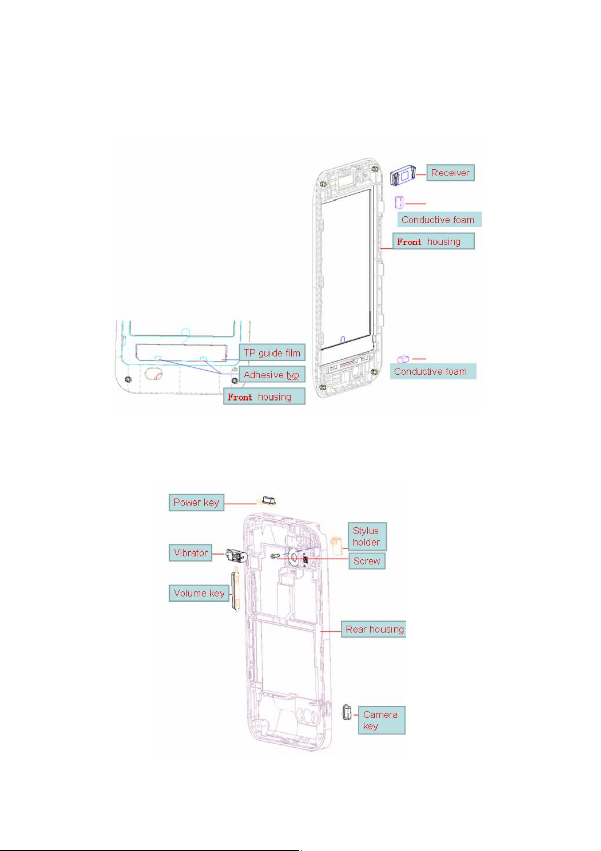
The following pictures describe the step to assemble
Step 1:Stick receiver into front housing Stick 2 conductive foams to
corresponding position Fixed TP guild flim
Step 2:Screw stylus holder into rear housing Install vibrator into rear housing
Install side keys
- 69 -
Page 70

Step 3:Welding the speaker Welding the MIC Welding the FPC of flash
LED
Step 4:Install the speaker into ANT stent and fix the stent(if the hook damaged
in installing ,add 2 screws) Install Wi-Fi ANT Stick flash LED
Connect camera and stick it
- 70 -
Page 71

Step 5:Welding the LCM
Step 6:Stick mylar and stick the LCM on main board Stick the stylus foam
- 71 -
Page 72

Step 7:Install main key into front housingStick the protective film on the metal
surface of front housingInstall TP Install the main board into front
housing
Step 8:Connect FPC into the TP connector
- 72 -
Page 73

Step 9:Stick mylar(size 6*10) on camera connectorStick mylar(size 6*6) on
welding pad of flash LED and TP connector
Step 10:Install rear housingscrew in the screws
- 73 -
Page 74

The echo loop tests the analog loop back path from MIC to Receiver.
Use LSK to turn on and off the analog loop back path. Remember to
keys are displayed
on the screen. When a key is pressed, the depression is detected and
the key disappears from the screen. Once all keys are detected, the
or
Press LSK to emit a 1 KHZ tone from the mobile; the tester can hear
the sound played. Use LSK to turn the sound on and off. Remember to
if the loudspeaker is operating properly when a melody is played.
Press LSK to play a 1 KHz tone. Use LSK to turn the tone on and off.
Test the analog loop back path from headset MIC to headset receiver.
Remember to turn off
8 Fly E175 Wi-Fi SELF TEST
From the idle screen, to enter Factory Mode, enter *#94683538# on the keypad. As in normal
menu operation, the Right Soft Key (RSK) "BACK" returns to the previous screen and the "END" key
returns to the idle screen.
Version
Software Version inside the phone can be found in this screen
Echo loop
turn off echo loop before testing other items.
Test all keypad keys including side keys. All the
Keypad
test stops and exits.
Vibrator
Use LSK to turn the vibrator on and off. Remember to turn the vibrat
off before testing other items.
Loudspeaker
Ring Tone
Receiver
Charger
Headset
turn the loudspeaker off before testing other items.
Test
Remember to turn the ring tone off before testing other items.
Remember to turn off the tone before testing other items
Test the Charge voltage and current
Use LSK to turn the analog loop patch on or off.
the loop back path before testing other items.
- 74 -
Page 75

9 Fly E175 Wi-Fi upgrading ROM procedure
Step 1 Com port number can be checked by device management as below:
Under COM and LPT item as Prolific USB-to-Serial Com Port. Com port number
will be used while setting software.
Step 2 The image code can be upgraded by Multi-port download tool as below:
Step 3 Multi-port download tool can be executed directly by click
"MultiPortFlashDownloadProject" file without any installation.
Step 4 When first executing program, the error message will be shown as below:
after setting MTK_AllOne_DA.bin from the program, the error message will disappear.
- 75 -
Page 76

Step 5 Run the
Operation setting, select to NFB
COM Port setting, select to UART
TYPE setting, select to Download ROM and Format
Format FAT Option setting, select to Auto
Baud Rate setting, select to 921600
- 76 -
Page 77

Step 6 Click "open Download Agent File" from File option manual.
Note: Please select COM port that Download cable has used such as COM3.
Different computer used different com port for download cable.
Com port number can be checked by device management as below:
Under COM and LPT item as Prolific USB-to-Serial Com Port.
- 77 -
Page 78

Step 7 Select MTK_AllInOne_DA file.
- 78 -
Page 79

Step 8 Click "Select Scatter and Load Setting" from File option manual.
Step 9 Select you want update of the file path & file (*.TXT) as below.
- 79 -
Page 80

Step 10 As picture below, if the path & file name is correct, it mean the setting will finish.
Step 11 Follow number as below to set parameter and then press start.
Note: please select download ROM only from Type manual.
- 80 -
Page 81

Step 12 Remove the battery and then reinstall it again, plug in USB cable then the update
procedure will be in progress.
Step 13 When progress is 100%, press stop button and close program.
- 81 -
 Loading...