

Page 1

E170(E950E) Service Menu
Version number: V1.0
Draft Hu Zhenhua
Auditing Liu Changling
Authorize Tang Yin
Date 2010-5-11
Longcheer Technology (Shanghai) Co., Ltd.
Page 2

Contents
1 Overview E170.........................................................................................................................1
1.1 About E170 Phone..............................................................................................................1
1.2 Distribution of the mainboard components.........................................................................2
2 RF.............................................................................................................................................3
2.1 RF Overview.......................................................................................................................3
2.2 Transmit..............................................................................................................................3
2.3 Receive................................................................................................................................3
2.4 Common RF Malfunction...................................................................................................4
3 Baseband................................................................................................................................15
3.1 Baseband Overview ..........................................................................................................15
3.2 Logic.................................................................................................................................15
3.3 Power management...........................................................................................................15
3.4 Audio Frequency...............................................................................................................16
3.5 Bluetooth circuit................................................................................................................17
3.6 Baseband common malfunction........................................................................................17
4 Reference for maintenance...................................................................................................21
4.1 No Signal ..........................................................................................................................21
4.2 Phone does not “power on”...............................................................................................21
4.3 LCD trouble ......................................................................................................................21
4.4 Sound trouble....................................................................................................................21
4.5 Keyboard malfunction.......................................................................................................21
4.6 Camera with flowery/blank screen....................................................................................21
5 Tools........................................................................................................................................22
5.1 LCT downloading Operation Manual...............................................................................22
5.2 LCT Repair tools Operation Manual.................................................................................22
5.3 LCT Unlock Operation Manual........................................................................................22
5.4 LCT write SN Operation Manual......................................................................................22
5.5 LCT Calibration Operation Manual..................................................................................22
5.6 LCT Testing Operation Manual ........................................................................................22
5.7 LCT Function testing Operation Manual..........................................................................22
5.8 Detailed maintenance program .........................................................................................22
Page 3
E170 Service menu
1 Overview E170
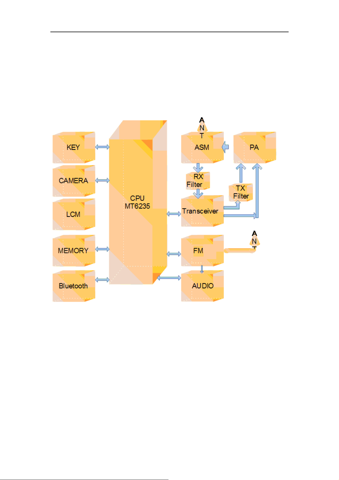
1.1 About E170 Phone
E170 mainboard is based on the MTK platform designed to support 3-band which
supporting the FM and Bluetooth calls and transmission, and analog TV, the mainboard
system consists of the base-band( CPUMT6235+MCPK5D1G12DCA) and the RF
(MT6140+PARPF89007).
1
Page 4
E170 Service menu
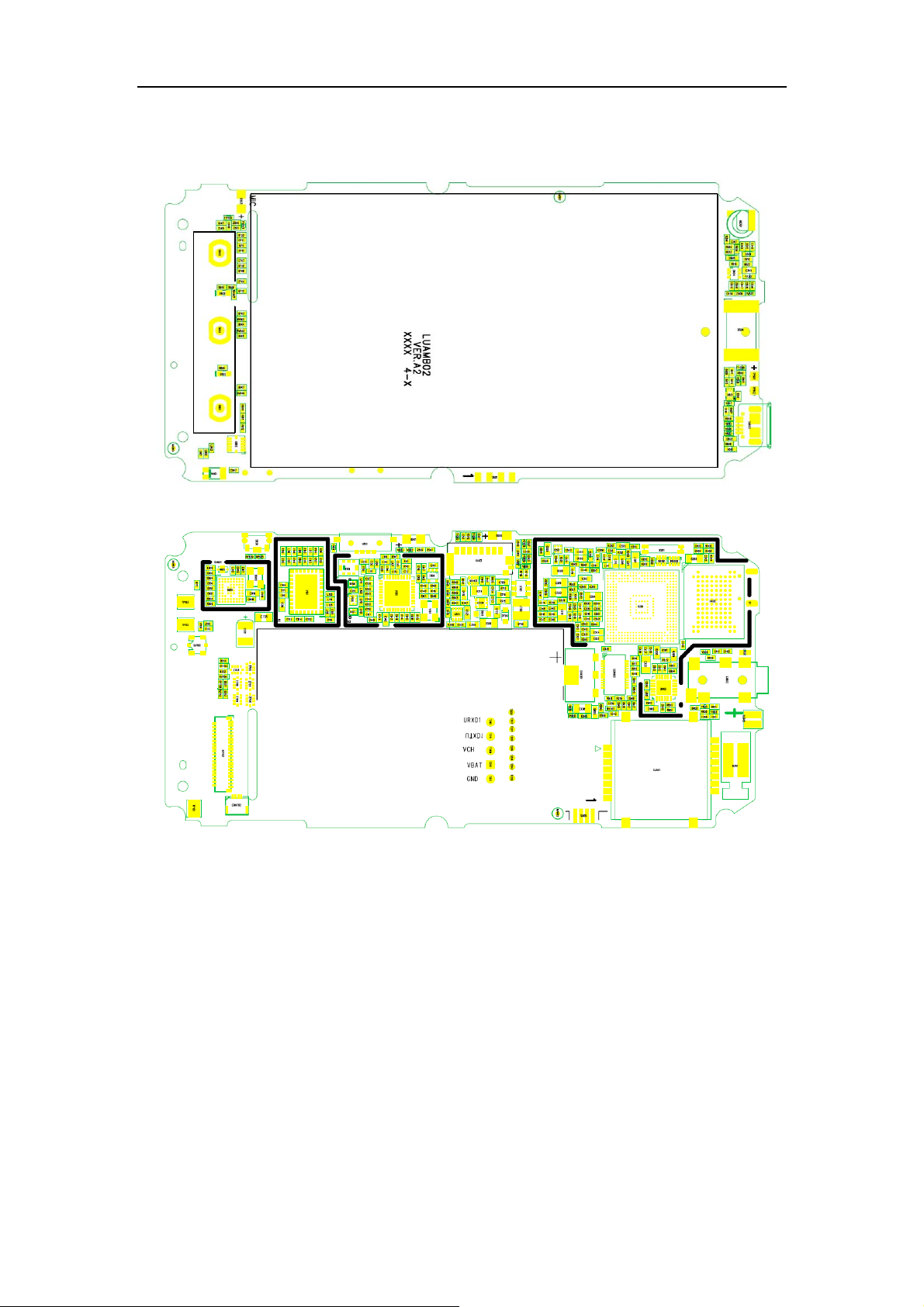
1.2 Distribution of the mainboard components
2
Page 5
E170 Service menu
2 RF
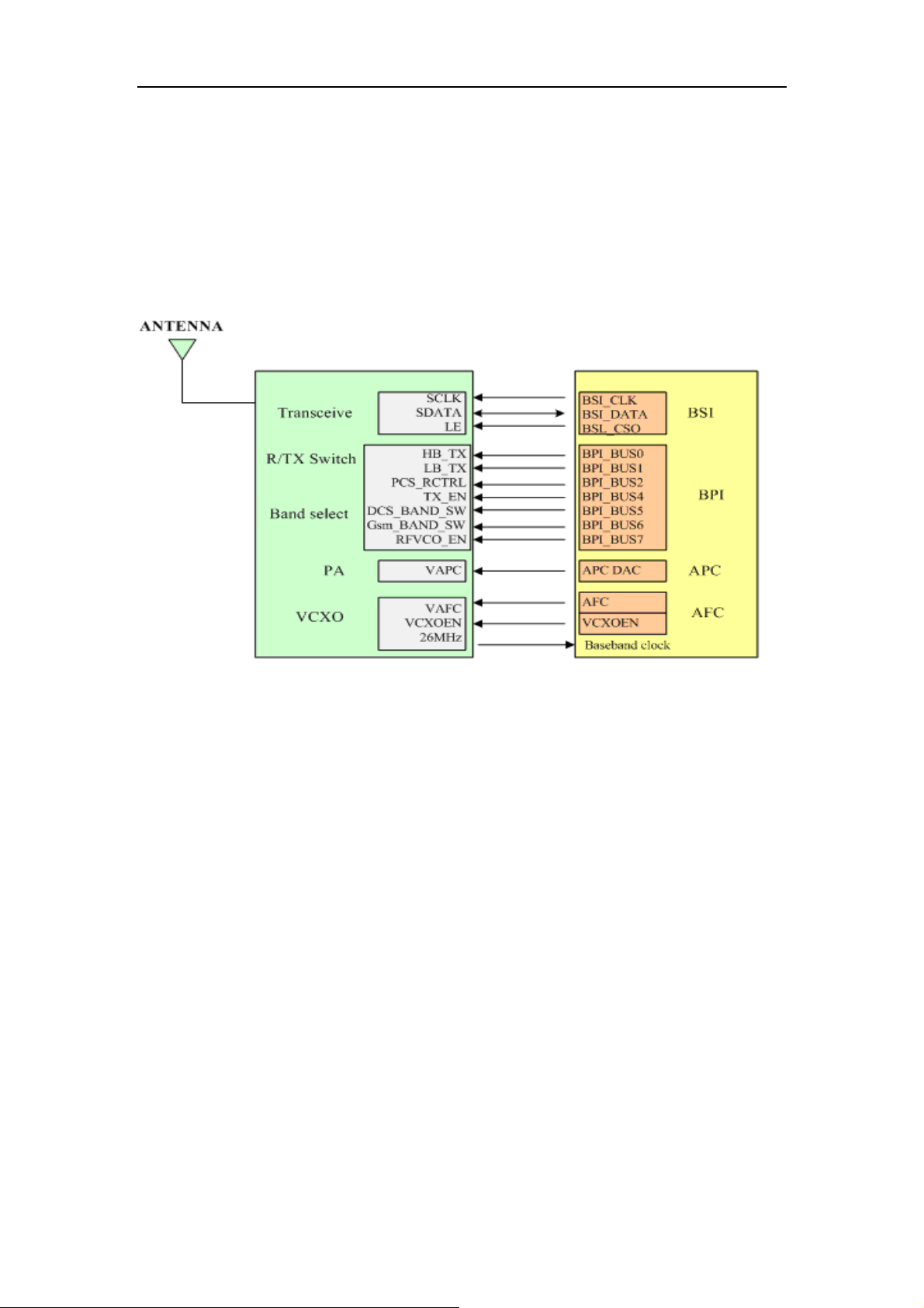
2.1 RF Overview
RF part mainly consists of transceiver MT6140 (adopts program of near-zero IF receiver,
supporting the EGSM / DCS and 26M VCTCXO as the clock input, integrated clock buffer,
LO VCO and TX VCO and regulator , only need for external connections of VBAT / AVDD),
P ARPF89007 (it supports EGSM / DCS / PCS and integrated automatic power control and
transceiver switch).
MT6140
Baseband Chip
GSM RF and BB interface diagram
Transceiver (MT6140) with the RF modulation and demodulation functions contains IF
frequency synthesizer and VCO RF, which is part of the core component of the RF. PA has
a major role in amplification of modulation signal, and it must be controllable and the
speed should meet the GSM agreement.
2.2 Transmit
TX is composed of the modulation loop, power amplifier and antenna switch. PLL is
mainly in the internal MT6140, I / Q signal first enters into the MT6140, after entering the
PLL the signal is modulated to RF, and then it out puts from the chip to PA, converts into
electromagnetic energy through antenna by the antenna switch after enlarged.
PA:
This part adopts voltage control to achieve and its role is to amplify the signal power in
accordance with the requirements. It is divided to two different power levels through
VRAMP signal. The transmit signal of GSM is 5 to 19, power is from 3.2MW to 2W while
DCS is 0 ~ 15, power from 1MW ~ 1W. PA is time-sharing work controlled by TX-EN chip,
the output power of PA is controlled by VRAMP (APC) through the voltage. PA is
intermittent work, by the BS to achieve the choice of frequency bands.
2.3 Receive
Antenna RX - MT6140 (RX_VCO mixer) - band-pass - Amplification - filter - Amplification RX_VCO mixer - CPU
3
Page 6
E170 Service menu
Check IQ si
g
p
2.4 Common RF Malfunction
2.4.1 Detection and Maintenance Flow Chart of MS Transmit
malfunction
(No transmit) Connect PC and cell
hone with maintenance of line, use the
Repair software making mobile phone
access to transmit state.
Y
Check antenna switch
or matching network
Y
pin of Transceiver,
whether there is IQ
si
nal?
gnal input
Y
Check RF signal
output pin, whether
there is any RF
Y
VBAT, PA_EN,
BANDSW_DCS,V
APC, are they OK?
N
N
Check CPU
N
Check Transceiver,
whether there is any
RF output signal?
N
Check
Transceiver
External
Y
Replace PA
Check CPU
Replace
Transceiver
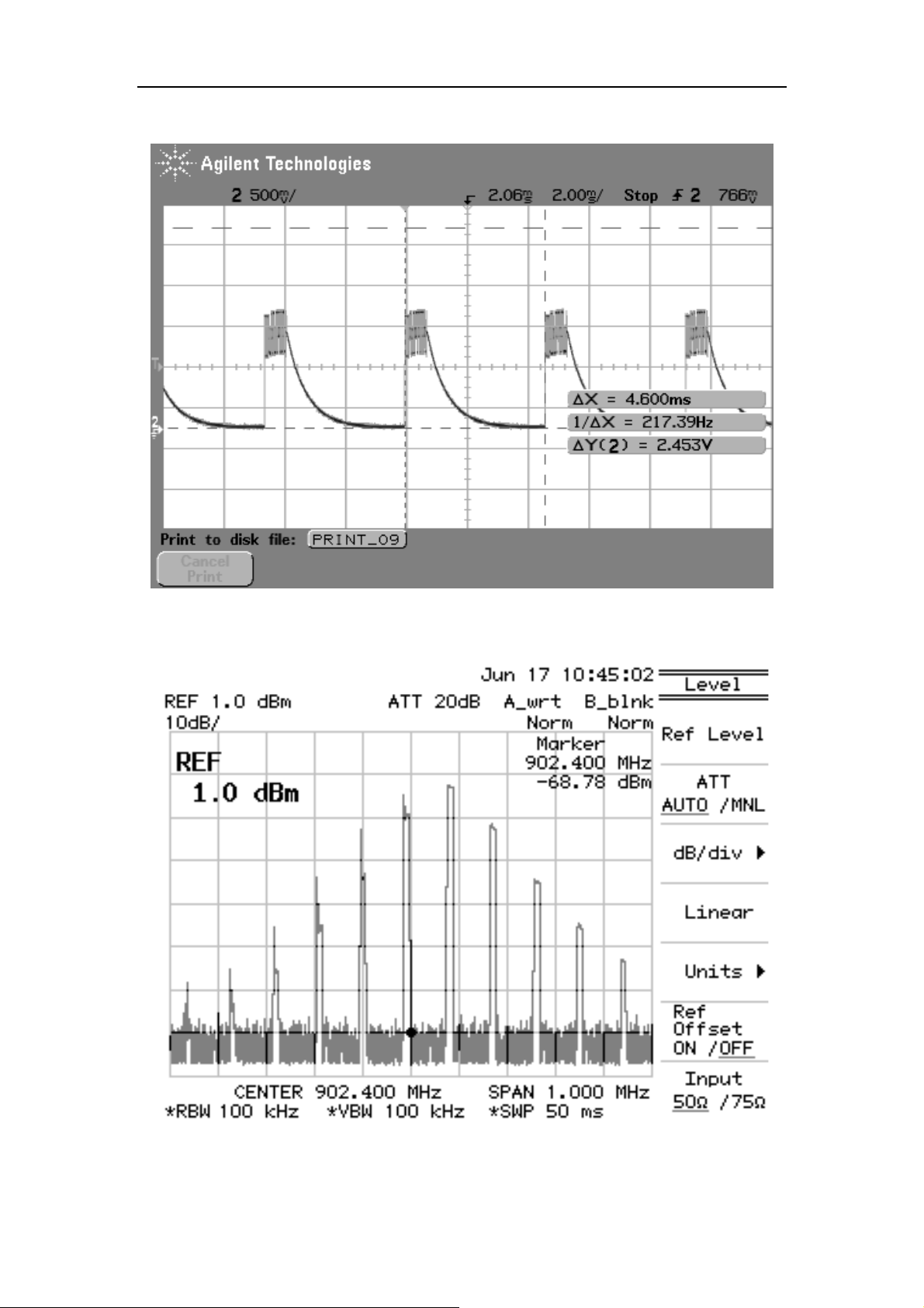
2.4.2 The maintenance process of Transmit malfunction
Use the Repair software making mobile phone access to transmit state. Choose 62CH in
GSM band, POWER Level for 5, DCS for 700CH, POWER Level for 0. Then, first observe
whether the current rises, and use the spectrum analyzer and oscilloscope to observe the
signal given in the above-mentioned flow chart, the specific signal waveforms shown as
below:
4
Page 7
E170 Service menu
IQ signal waveforms of transceiver in transmit state:
3.10 IQ
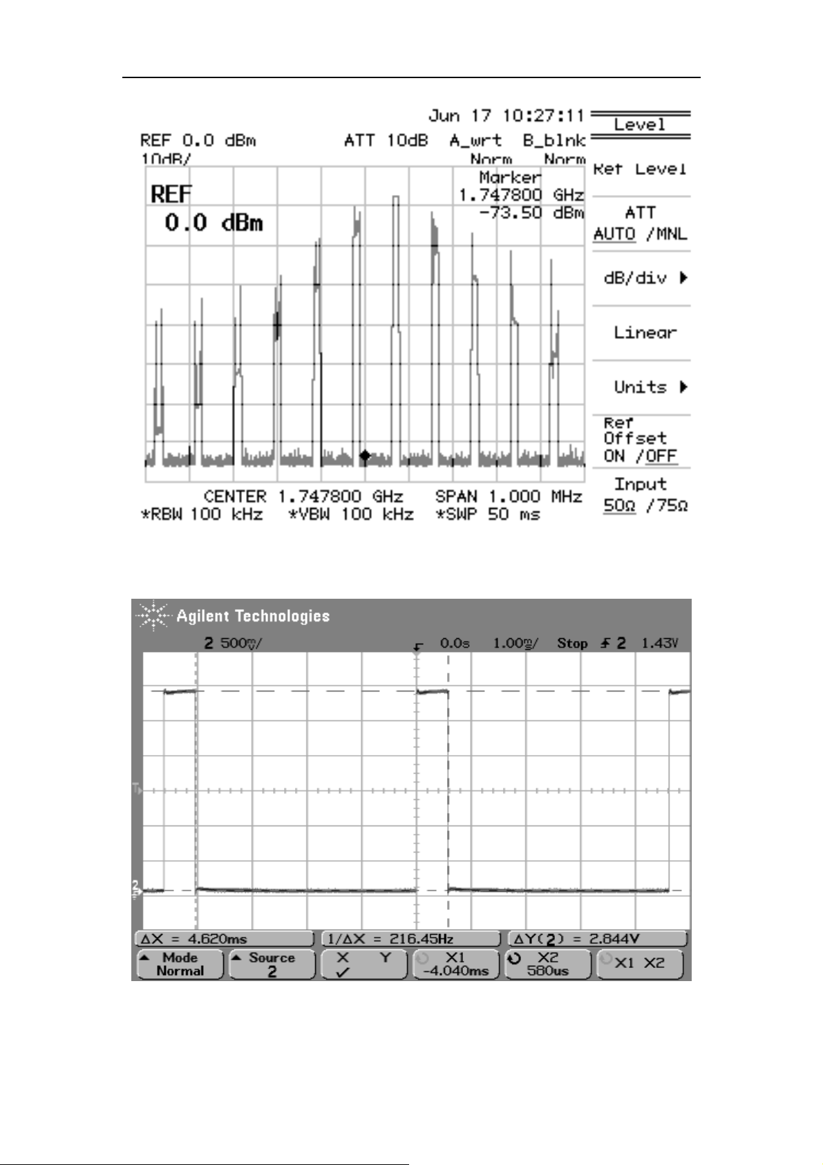
RF interface spectrum analyzer is as follows:
GSM transmit signal
5
Page 8
E170 Service menu
DCS transmit signal
PA-EN waveforms of PA in transmit state:
PA-EN
6
Page 9

E170 Service menu
PA. BAND-SW waveforms:
PA.BAND-SW (GSM)
PA.BAND-SW (DCS)
7
Page 10

E170 Service menu
PA Vramp waveforms:
Vramp (pcl5)
Vramp (pcl 19)
8
Page 11

E170 Service menu
g
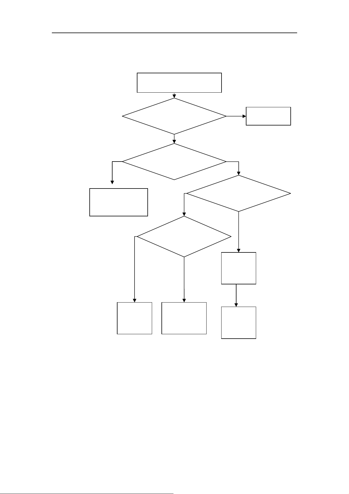
2.4.3 Detection and Maintenance Flow Chart of MS Receive
malfunction
No Receive
Open Repair Software to connect PC with mobile phone, make the
phone access to receiving state, adjust signal generator to
corresponding CH, and connect the signal line to phone’s RX_SW.
Check IQ signal output pin
Y
Check MT6235
Y
of Transceiver, whether
there is IQ signal?
N
Check Transceiver input
pin, whether there is any
input signal?
N
Are Transceiver
SDATA、 SCLK、
LE、RFVCOEN all
correct?
N
Whether PA signal
input pin has
received any
nal?
si
N
Check or replace the
antenna switch and
matching circuits
Y
Check RX-filter
Check Transceiver
External RC components
Check CPU
N
Check the
correspondi
ng power
supply and
circuits of
26MHZ.
Y
Whether the voltage
Transceiver used is
normal? Is 26MHz
normal?
Y
Replace
Transceiver
2.4.4 The maintenance process of Receive malfunction
Maintenance process of NO Receive: Use Repair software to make mobile phone access
to pure receive state → Choose 62CH, Rx Mode CH62=94 7.4MHZ, Input power:-60dbm
in GSM frequency bands → Choose 698CH, Rx Mode CH698=1842.4MHZ, Input
power:-60dbm in DCS frequency bands → Adjust signal generator to corresponding CH,
connect the signal line to Cable of RF → Measure the related key signal by using
Spectrum analyzer and Oscilloscope → Measure the signal output pin of Transceiver,
whether there is any correct IQ signal output to CPU → Y: Check CPU (MT6235) / N:
Check Transceiver input pin, whether there is any corresponding CH input signal (Y:
Check whether Transceiver has correctly controlled the signal → Check whether the
9
Page 12

E170 Service menu
voltage supply is normal → if normal, Transceiver can be judged of damaged / N: Check
PA and the paths ahead )
Signal waveforms refer to the following:
Output signal of Signal generator (Input):
GSM CH62 channel receives the signal
DCS CH 698 channel receives the signal
10
Page 13

E170 Service menu
IQ signal output pin of Transceiver the state of receiving IQ signal:
The signal Transceiver received from CPU used to access the internal register of
Transceiver. The corresponding waveform is as follows:
IQ Signal
Frequency-s
ynthesizing
signal
11
Page 14

E170 Service menu
3W(SDATA)
3W(SCLK)
12
Page 15

E170 Service menu
3W(LE)
26M clock (can be measured by using the ACCoupling)
The AFC (automatic frequency control) from CPU to the crystal oscillator makes crystal
oscillator output accurate 26MHZ to Transceiver.
26M Output
26M
Input
13
Page 16

E170 Service menu
VAFC
TCXO output(26MHZ)
14
Page 17

E170 Service menu
3 Baseband
3.1 Baseband Overview
E170 Baseband consists of CPUMT6235 and Program Memory . UMT6235 baseband, the
core device of the mainboard, is responsible for the normal work among various parts of
mainboard, such as voice processing, image processing, power management as well as
MS communications.
UMT6235 digital baseband contains 32-bit ARM7E core and 284Kbyte SRAM. UMT6235
which is an enhanced GSM Processor integrated Channel Codec subsystems interiorly
including Channel Codec, Intertlace / Deinterleave, Encryption / Decryption and Control
Processor subsystems including ARM7EJS and its peripheral circuits. There are 26
address lines,16 data lines, 8 chip select lines, provided 6 external interrupt Interface,
26M/52M operation clock.
Analog baseband contains UMT6235 analog baseband chip, audio, baseband codec and
power management. Four major functional blocks integrated internal: Audio codec
including Voice input / Output channel, Buzzer output; Baseband codec including
Differential I, Q input / output, GMSK modulation and A / D, D / A; Auxiliary parts including
AFC DAC, RAMP DAC, AGC DAC and a seven-channel A / D. And WATCHDOG interface
is set internal to enhance the stability of the system.
3.2 Logic
Logic part is composed of MTK base-band management chip UMT6235, power
management chip MT6235 and Nand Flash.
UMT6235:CPU
Nand Flash:
MT6235:PMU
3.3 Power management
Power management consists of the charging circuit integrated in MT6235 and the external
charging circuit. It provides 11 road LDO voltage. Besides, it completes the logic level
conversion of SIM card. The chip also outputs the system reset signal.
15
Page 18

E170 Service menu
Boot process:
The normal boot is to press boot key which is that the PWRKEY is being dragged down.
Once the boot key is pressed, all LDO are open except VSIM. After VCORE opening
RESET timer and timer out, RESET is being pitched up to start the digital baseband chip,
that is, UMT6235 starts to run and roll polling its ROWX pin, pitch up its PWRONIN pin,
then you can release the boot key. This is the initial boot process.
3.4 Audio Frequency
The sound quality performs more pleasant on account of audio processing integrated in
UMT6235.
3.4.1 Speaker loop
3.4.2 MIC loop
Check basic bias voltage signal of MICBIASP and MICBIASN and the language signal of
MIC itself when the MIC is good but no response of LOOP MIC in test.
16
Page 19

E170 Service menu
3.4.3 Earphone loop
Earphone loop includes headset speaker and MIC two-way signal. Check the circuit
access situation when there is something abnormal (such as: no sound in headset
speaker, Mic invalid, etc.) after inserting the earphone while the headset accessories are
good.
3.5 Bluetooth circuit
Bluetooth is a design feature of this cellphone. It is with a matching Bluetooth headset and
the phone has a container which can charge up Bluetooth headset through the main
board, to accommodate Bluetooth headset. Some of the projects may not have this
function, however, the mainboard is compatible. Please first ensure that the power is
correct, according to the phenomenon and following schematic diagram to maintain the
phone.
Bluetooth circuit
3.6 Baseband common malfunction
3.6.1 Nand Flash programming does not download
Data lines used for downloading software: VBA T, TX, RX, GND, CHARGE. It is mostly due
to the false solder and wire bonding. First check whether the serial port of PC and cell
phone is unrestricted, if not, it is caused by being lack of devices or empty solder of power
manager, USB-con and peripheral resistance. Measure the TX, RX signals by using
AC-coupled oscilloscope to track the signal flow, if a certain period circuit of no signal it
may be AC short circuit to ground, or is caused by a short circuit and open circuit. On
checking the malfunctions, first should carefully observed the welding of these devices
with a magnifying glass, then plug in the download line to observe whether the current is
normal, there is short-circuit to ground of VCHG or VBAT if the current is large, at this time
17
Page 20

E170 Service menu
N
cut off power supply as soon as possible, and then find the short-circuit point. It may be
the abnormal output power supply of a certain circuit that the current is larger than normal
(about 30 mA) but not particularly large, at this time should check whethe the valgate of
VCORE (1.8V), VDD (2.8V), VADD (2.8 V), VTCXO (2.8V), VRTC (1.5V), VMEM (2.8V) is
noamal, if not, bad welding can be detected. Focus on checking the welding of PMU and
USB-CON if there is a little or no current. Unplug and re-plug the download line to see if it
is caused by poor contact; It can test that whether the output of 26MHz clock signal to the
CPU is normal by using oscilloscope.
3.6.2 Detection and Maintenance Flow Chart of No download
malfunction
Not download
Eliminate any
reasons for not
Yes
download except
the cell phone.
Check whether the
5pin connector
USB-CON is false
soldered or
NO
Check whether it is the problems
of allocation of procedure,
download cable, power supply,
software, PC phone.
Check whether the serial port of
PC and cell phone is unrestricted.
damaged.
NO
Check USB-con
peripheral
resistance
Connect the download line and
observe the ammeter whether the
current is high (normal current is
generally about 30mA).
A little or no current
Check whether the voltage supply of CPU
power manager, PMU and LDO is normal,
whether there is any power supply open circuit.
NO
Yes
Yes
ormal current but no download
Check VCORE 、 VDD 、 VAD D 、
VTCXO、VRTC、VMEM、measure the
clock signals of 26MHZ、32KHZ
Quickly disconnect the
connection, and touch
the chip gently to see if
it is hot, if not, focus on
measuring the
short-circuit point by
using multimeter.
Check whether CUP and NORFLASH
is OK, LDO is normal?
18
Page 21

E170 Service menu
3.6.3 The signal waveform
Chip select signals CS:
Screen reset signal LRST:
19
Page 22

E170 Service menu
Screen Write signal LWR:
About the screen, first find the problem whether is mainboard or screen by adopting
replacement method, then focus on checking the LCM-CON welding.
20
Page 23

E170 Service menu
4 Reference for maintenance
4.1 No Signal
The common processors: Transceiver, PA.
4.2 Phone does not “power on”
The phone can not power on is usually caused by false welding. First need to check the
signal integrity of 26MHZz, 32.768KHz as well as the continuity of signal path. Then check
the integrity of core voltage and path. Generally, CPU will less be damaged, and it is due
to smaller current but normal voltage, at this time Replacement method should be adopted,
and try to add more welding, re-welding.
4.3 LCD trouble
Re-welding display interface and nearby resistance row, as if it is still abnormal, check the
pad whether it is of short circuit.
4.4 Sound trouble
E170 audio processes in internal CPU, focus on checking the Audio-PA on the issue of
free or miscellaneous ring tones. Low ring for checking its solder joints (very small, and
easy to cause problems). Try more times for re-welding and replacement.
4.5 Keyboard malfunction
In most cases there is something wrong with the linking of single button with circuitry if
only this button does not work. Focus on checking the resistance row near the display or
whether CPU is short circuit if group buttons do not work.
4.6 Camera with flowery/blank screen
First check the Interface whether there is any false solder, and check peripheral devices
whether lack of devices.
Note: The waveforms may be different according to the settings and different devices in
maintaining.
21
Page 24

E170 Service menu
5 Tools
5.1 LCT downloading Operation Manual
Reference:《手机软件下载操作说明_MTK_售后版》
5.2 LCT Repair tools Operation Manual
Reference:《维修软件操作说明_MTK_》
5.3 LCT Unlock Operation Manual
Reference:《解手机锁软件操作说明_MTK_》
5.4 LCT write SN Operation Manual
Reference:《写生产序列号操作说明_MTK_》
5.5 LCT Calibration Operation Manual
Reference:《双回路校准系统操作说明_MTK_》
5.6 LCT Testing Operation Manual
Reference:《双回路综测系统操作说明_MTK_》
5.7 LCT Function testing Operation Manual
Reference:《主板功能测试软件操作说明_MTK_》
5.8 Detailed maintenance program
Reference: 《MTK 平台维修手册 V1.0》
22
 Loading...