

Page 1

E146_Maintenance Instruction
Prepared by:xiaoyu wan
Approved by:
Date:2010.9.28
Page 2

TABLE OF CONTENTS
1 Overview E146
1.1 About E146 Phone
1.2 Distribution of the mainboard components
2 RF
2.1 RF Overview
2.2 Transmit
2.3 Receive
2.4 Common RF Malfunction
3 Baseband
3.1 Baseband Overview
3.2 Logic
3.3 Power management
3.4 Baseband common malfunction
4 Reference for maintenance
4.1 No power on
4.2 Shut off automatically
4.3 Dead halt
4.4 No charge
4.5 Quantity of electricity faulty detection
4.6 No display
4.7 LED NG (on the LCD)
4.8 LED NG (on the keyboard)
4.9 Key NG
4.10 No ring
4.11 No receiving voice
4.12 No sending voice or voice is small
4.13 No vibration
4.14 SIM card inefficacy
4.15 TF card inefficacy
4.16 Camera inefficacy
4.17 Bluetooth inefficacy
4.18 Earphone inefficacy
4.19 FM inefficacy
4.20 G sensor inefficacy
Page 3
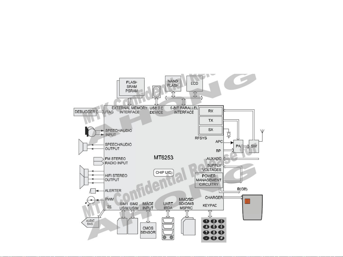
1 Overview E146
1.1 About E146 Phone
E146 mainboard is based on the MTK platform designed to support 2-band
which supporting the FM and Bluetooth calls and transmission, the
mainboard system consists of the base-band (CPU:
MT6253+PF38F4050M0Y3DEA) and the RF (MT6253+RF7161).
Page 4
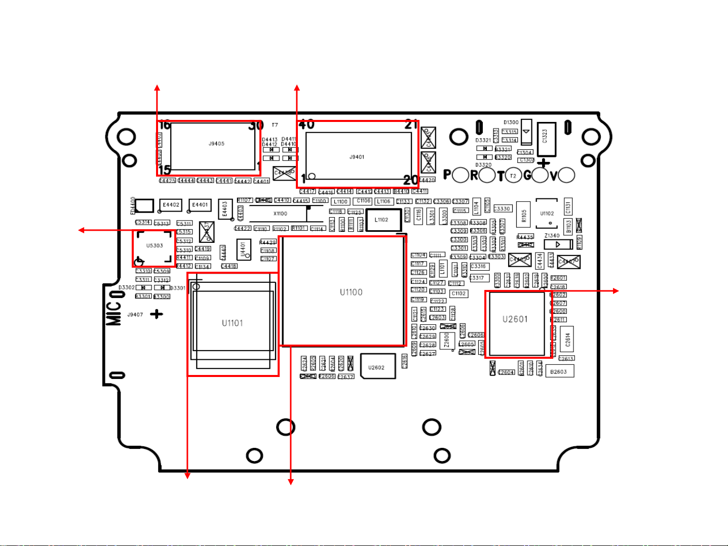
1.2 Distribution of the mainboard components
FM
TY6701111184KC
Camera FPC
RDA5802ES
MT6253
LCD CON
MT6253
RF7161
RF PA
Flash
CPU
Page 5
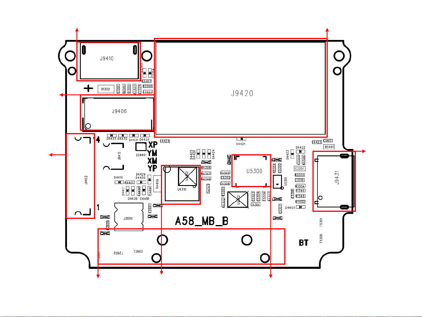
Socket of T card
Socket of SIM card Battery CONN
K/B FPC
Antenna
MXC62025MP
G-senser
Adapter CONN
MT6612
BT area
Page 6

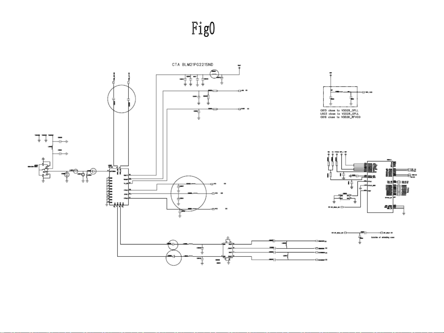
2 RF
2.1 RF Overview
RF part mainly consists of transceiver MT6253 (adopts program of near-zero IF
receiver, supporting the EGSM / DCS and 26M VCTCXO as the clock input,
integrated clock buffer, LO VCO and TX VCO and regulator, only need for
external connections of VBAT / AVDD), RF7161 (it supports EGSM / DCS
and integrated automatic power control and transceiver switch).
Transceiver (MT6253) with the RF modulation and demodulation functions
contains IF frequency synthesizer and VCO RF, which is part of the core
component of the RF. PA has a major role in amplification of modulation
signal, and it must be controllable and the speed should meet the GSM
agreement.
Page 7

2.2 Transmit
TX is composed of the modulation loop, power amplifier and antenna
switch. PLL is mainly in the internal MT6253, I / Q signal first
enters into the MT6253, after entering the PLL the signal is
modulated to RF, and then it outputs from the chip to PA, converts
into electromagnetic energy through antenna by the antenna
switch after enlarged.
PA:
This part adopts voltage control to achieve and its role is to amplify
the signal power in accordance with the requirements. It is divided
to two different power levels through VRAMP signal. The transmit
signal of GSM is 5 to 19, power is from 3.2MW to 2W while DCS is
0 ~ 15, power from 1MW ~ 1W. PA is time-sharing work controlled
by TX-EN chip, the output power of PA is controlled by VRAMP
(APC) through the voltage. PA is intermittent work, by the BS to
achieve the choice of frequency bands.
2.3 Receive
Antenna RX - MT6253 (RX_VCO mixer) - band-pass - Amplification -
filter - Amplification - RX_VCO mixer - CPU
Page 8
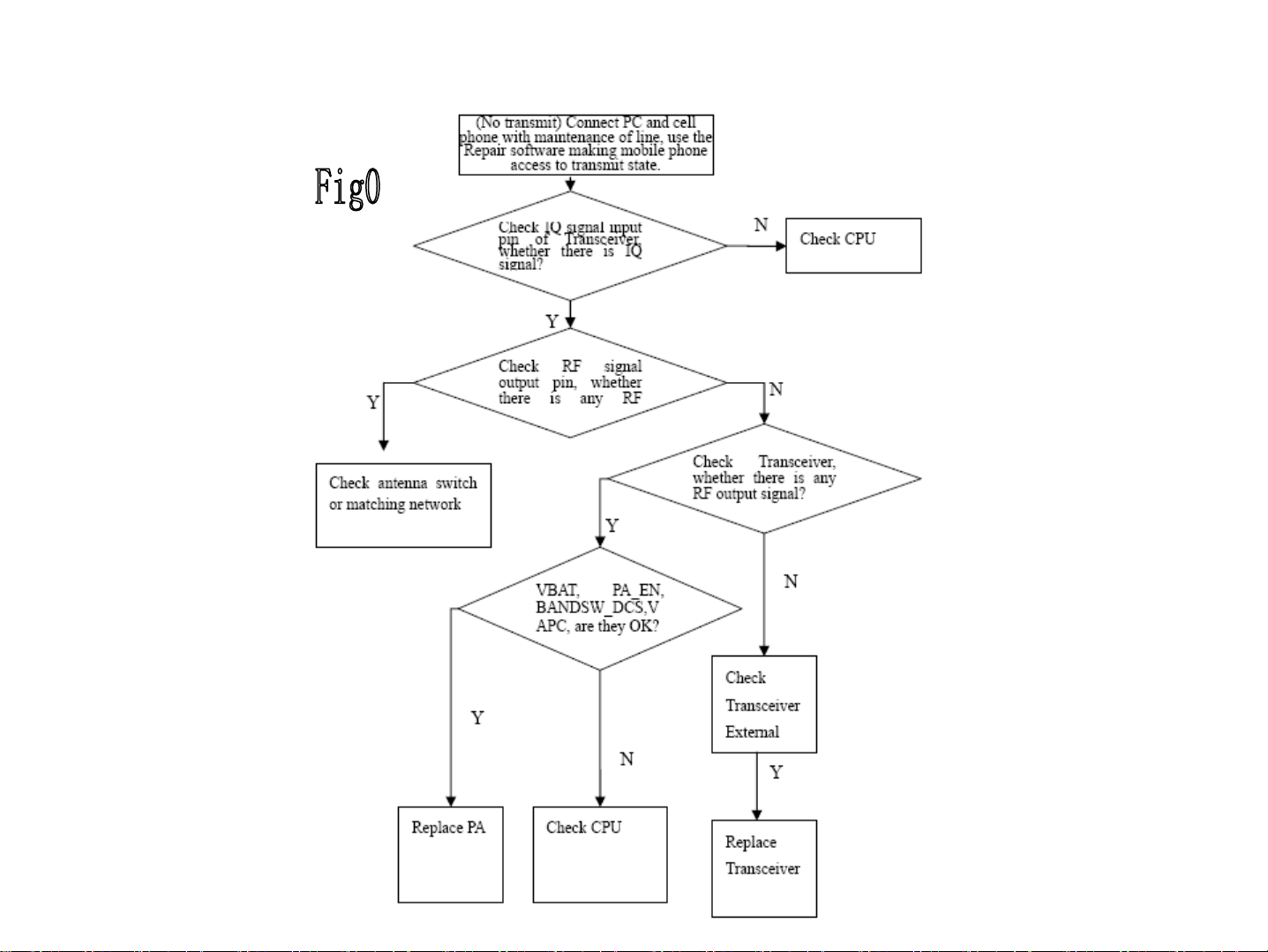
2.4 Common RF Malfunction
Detection and Maintenance Flow Chart of MS Transmit malfunctio
Page 9
Page 10

3 Baseband
3.1 Baseband Overview
E146 Baseband consists of CPU MT6253 and Program Memory. MT6253
baseband, the core device of the mainboard, is responsible for the normal work
among various parts of mainboard, such as voice processing, image processing,
power management as well as MS communications.
MT6253 digital baseband contains ARM7EJ-S 32-bit core and 144Kbyte SRAM.
MT6253 which is an enhanced GSM Processor integrated Channel Codec
subsystems interiorly including Channel Codec, Intertlace / Deinterleave,
Encryption / Decryption and Control Processor subsystems including ARM7EJ-S
and its peripheral circuits. There are 25 address lines,16 data lines, 8 chip select
lines, provided 7 external interrupt Interface, 52M/104M operation clock.
Analog baseband contains MT6253 analog baseband chip, audio, baseband
codec and power management. Four major functional blocks integrated internal:
Audio codec including Voice input / Output channel, Buzzer output; Baseband
codec including Differential I, Q input / output, GMSK modulation and A / D, D / A;
Auxiliary parts including AFC DAC, RAMP DAC, AGC DAC and a seven-channel
A / D. And WATCHDOG interface is set internal to enhance the stability of the
system.
Page 11

3.2 Logic
Logic part is composed of MTK base-band management chip MT6253, power
management chip MT6253 and Nor Flash.
CPU : MT6253
Nor Flash:PF38F4050M0Y3DEA
PMU : MT6253
3.3 Power management
Power management consists of the charging circuit integrated in MT6253 and the
external charging circuit. It provides 11 road LDO voltage. Besides, it completes
the logic level conversion of SIM card. The chip also outputs the system reset
signal.
Page 12
Boot process:
The normal boot is to press boot key which is that the PWRKEY is being dragged down.
Once the boot key is pressed, all LDO are open except VSIM. After VCORE opening RESET
timer and timer out, RESET is being pitched up to start the digital baseband chip, that is,
UMT6253 starts to run and roll polling its ROWX pin, pitch up its PWRONIN pin, then you can
release the boot key. This is the initial boot process.
Page 13

3.4 Baseband common malfunction
3.4.1 Nor Flash programming does not download
Data lines used for downloading software: VBAT, TX, RX, GND, CHARGE. It is
mostly due to the false solder and wire bonding. First check whether the serial port
of PC and cell phone is unrestricted, if not, it is caused by being lack of devices or
empty solder of power manager, USB-con and peripheral resistance. Measure the
TX, RX signals by using AC-coupled oscilloscope to track the signal flow, if a
certain period circuit of no signal it may be AC short circuit to ground, or is caused
by a short circuit and open circuit. On checking the malfunctions, first should
carefully observed the welding of these devices with a magnifying glass, then plug
in the download line to observe whether the current is normal, there is short-circuit
to ground of VCHG or VBAT if the current is large, at this time cut off power supply
as soon as possible, and then find the short-circuit point. It may be the abnormal
output power supply of a certain circuit that the current is larger than normal
(about 30 mA) but not particularly large, at this time should check whethe the
valgate of VCORE (1.8V), VDD (2.8V), VADD (2.8 V), VTCXO (2.8V), VRTC
(1.5V), VMEM (2.8V) is noamal, if not, bad welding can be detected. Focus on
checking the welding of PMU and USB-CON if there is a little or no current.
Unplug and re-plug the download line to see if it is caused by poor contact; It can
test that whether the output of 26MHz clock signal to the CPU is normal by using
oscilloscope.
Page 14
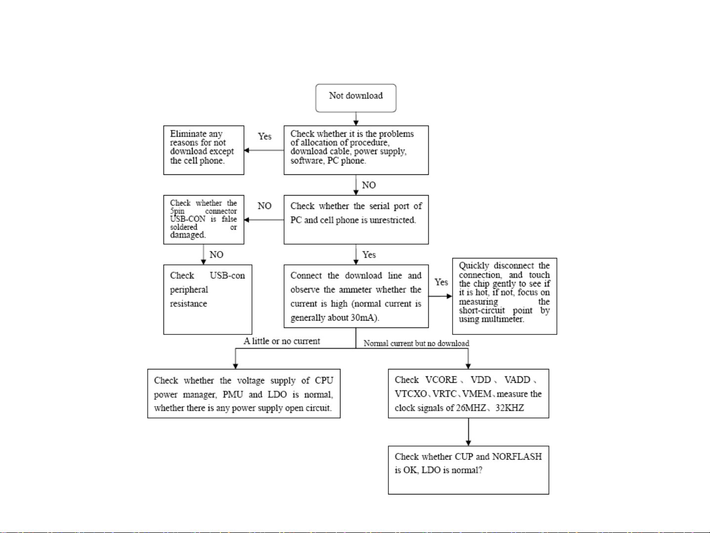
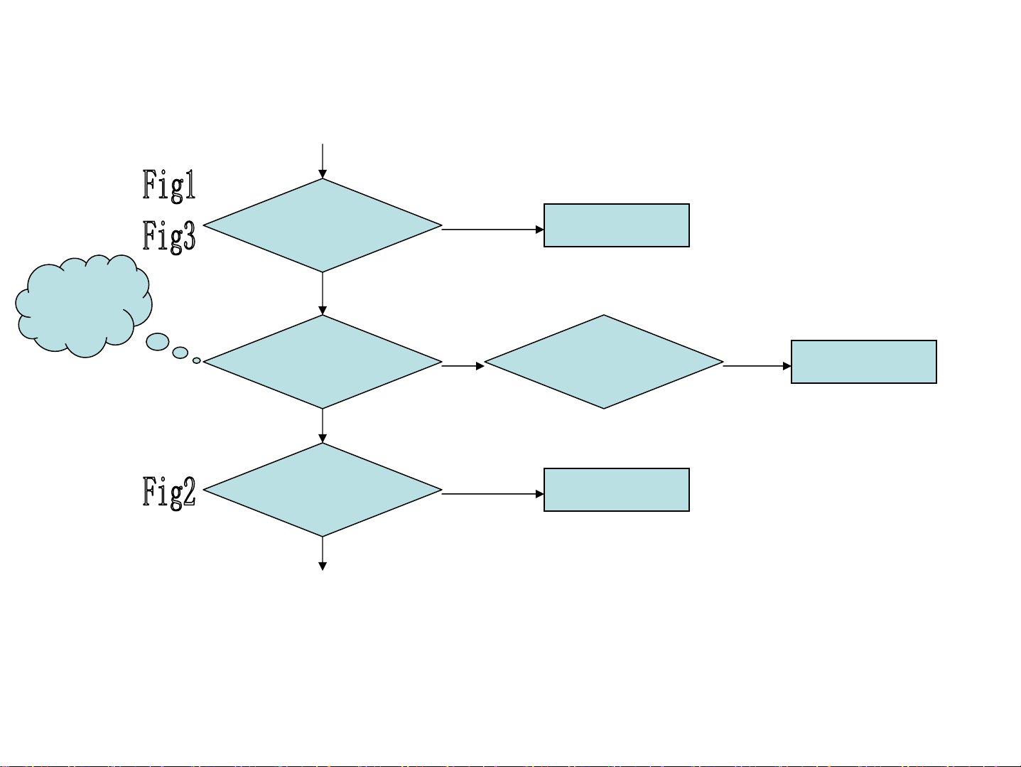
3.4.2 Detection and Maintenance Flow Chart of No download malfunction
Page 15
4 Reference for maintenance
4.1 No power on
No power on
Check whether the
battery voltage is
higher than 3.4V
Y
Check whether the battery
and the key pad is
oxidized or there is
anything else on it
N
Check whether the
connection of KEY PCB &
MB is OK
Y
Take out the LCD and
SPK, Check whether it is
powered on
N
Y
N
Y
Charge the battery
Wipe off the thing
or clean the key pad
Reassemble or Charge
the KEYPAD FPC
Cross-testing the
LCD&SPK,
Change the defective
N
Page 16
C1119:1.8V
C1119:2.8V,
C1120:2.8V,
C1121:2.8V,
C1122:2.8V,
C1123:2.8V,
Check whether
R4401,R1107 is
broken
N
Connect with the battery,
press “ON” key, check
whether the output voltage
of U1100 is normal
Y
Y
Change R4401,R1107
Replace the earthed capacitor
NN
corresponding to the
defective pin, Check whether
ChangeU1100
it is OK
Check whether the output
frequency of X1100 is 32.768K
Y
N
ChangeX1100,
C1100,C1101
Page 17
Check whether the output voltage
of U2602 pin 3 is 0.5V around
Y
N
Change U2602
N
Change U2605
Change the Flash (U1101),
check whether it is OK
Y
ChangeU1100
OK
N
Change U1101
Page 18
Page 19
Page 20
4.2 Shut off automatically
Shut off automatically
D/L the latest software,
Check whether it is OK
N
Replace with a
good battery, Check
whether the
primary cell is broken
N
Check whether the
rubber, used to fix the
battery, is lost or at the
other location
N
Check whether the battery
and the Connector of J9410 is
oxidized or there is
anything else on them
Y
Y
Y
Y
ok
Change the battery
Reassemble the
rubber
Wipe off the thing
or clean the Connector
N
Page 21

N
Check whether the contact of
the key PAD & the dome is OK
Y
Check whether X1100
output frequency is
32.768K exactly
Y
Refer to the maintenance
method of ‘No power on’
OK
N
N
Reassemble the dome
ChangeX1100,
C1113,C1114
Page 22

Page 23

4.3 Dead halt
Dead halt
D/L the latest software,
Check whether it is OK
N
Replace with a good
battery, Check whether
the primary cell is broken
N
Check whether the
problem is resulted
from ‘KEY NG’
N
Check whether the
problem is resulted
from the LCD itself
Y
Y
Y
Y
ok
Change the battery
Clean the K/B,
reassemble or change
the metal dome
Change the LCD
N
Page 24

Check whether the
output frequency of
X1100 is 32.768 exactly
Y
N
ChangeX1100,
C1113,C1114
Check whether the contact of
the key PAD & the dome is OK
Y
Replacing with the
programming FLASH,
check whether it is OK
N
Refer to the servicing
method of ‘No power on’
N
Reassemble
the dome
OK
Page 25

4.4 No charge
No charge
Replace with a good
adaptor, Check
whether the primary
adaptor is broken
N
Replace with a
good battery, Check
whether the
primary cell is broken
N
Check whether the
battery connector ‘J9410’
is oxidized or is broken
N
Check whether the
Micro USB ‘J9431’
is oxidized or is broken
Y
Y
Y
Y
Change the adaptor
Change the battery
Clean or
change J9410
Clean or
change J9431
N
Page 26

Plug in, Check whether it has an
voltage of 5V on B1103
Y
N
Change B1103
BLM18EG221TN1
Check whether there is broken of
U1102, R1105,C1131, Z1340
N
ChangeU1100
OK
Y
Change the defective
Page 27

4.5 Quantity of electricity faulty detection
Quantity of electricity
faulty detection
Replace with a good battery,
Check whether the primary cell
is broken
N
Format and Download the latest
Software, then calibrate the
ADC
N
Check whether there is broken
of D1300
N
ChangeU1100
Y
Change the battery
Y
Change the defective
OK
Page 28

4.6 No display
No display
Download the latest Software,
Check whether it is OK
N
Check whether the LCD is
weakly welded or broken
N
ChangeU1100
OK
Y
Y
ok
Re-weld or change
the LCD
Page 29

Page 30

4.7 LED NG (on the LCD)
LED NG (LCD)
Check whether the
LCD is broken
N
Check whether
C4400 C4402 C4441~C4444
is broken
N
Check whether
L1106 L1102 C1132 C1133
is broken
N
ChangeU1100
Y
Change the LCD
Y
Change U4400
Y
Change U4400
OK
Page 31

Page 32

4.8 LED NG (on the key board)
LED NG (key)
Checking method:
Crosstesting
the two sides of
LED by Multimeter ,
gearing to the short circuit,
if the LED is on at one
direction, it shows good
Check whether there
is anything (or Mylar)
on the key
N
Check whether the
LED of the KEYPD is
weakly welded or
broken
N
Check whether the
resistor beside the
LED is broken
N
Y
Y
Y
Clean or wipe off
the thing
Re-weld or
change the LED
Change the resistor
Page 33

Check whether the
connection of sliding PCB &
MB is OK
Y
N
Reassemble or Charge
the sliding FPC
Check whether
R4409 C4490 C4491
is broken
N
Check U1100
OK
Y
Change R4409 C4490
C4491
Page 34

Page 35

4.9 Key NG
Key NG
Check whether there is
anything oxidized or
smudge on the key pad
N
Check whether the
metal dome is oxidized
or broken
N
Check whether the
connection of KEY PCB &
MB is OK
Y
Y
Y
N
cleaning the key pad
Change the
metal dome
Reassemble or Charge
the KEY FPC
Page 36

Check whether the
D4417~D4420 D4429~D4434
is broken
N
Change CPU(U1100)
OK
Y
Change the defective
Page 37

4.10 No ring
No ring
Checking methodtesting
the resistance of the SPK
by Multimeter, gearing to
the resistance, the
resistance of it is 8ohm
normally
D/L the latest edition,
Check whether it is OK
N
Check whether the connection
of J9401 is OK
Y
Check whether the
SPK is void-welded
or broken
N
Check whether L3300 L3301
B3307 B3308 C3306 C3307
C3322 C3323 D3304 D3305
N
Y
N
Y
ok
Reassemble the
Connector
Re-weld or
change the SPK
Y
Change the defective
Change the CPU
OK
Page 38

Page 39

4.11 No receiving voice
No receiving voice
Checking methodtesting
the resistance of the REC
by multimeter, gearing to
the resistance, the
resistance of it is 30ohm
around
D/L the latest edition,
Check whether it is OK
N
Check whether the connection
of J9401 is OK
Y
Check whether the
REC PAD is oxidized
or broken
N
Check whether the
C3313~3315 B3320 B3321
D3320 D3321 is broken
N
Y
Y
N
Y
Ok
Reassemble the
Connector
Clean or
Change the REC
Change the defective
Change the CPU
OK
Page 40

Page 41

4.12 No sending voice or the voice is small
No sending voice
or a small voice
Checking method
testing the resistance of
the MIC by multimeter,
gearing to the resistance,
the positive resistance of
it is 1K, the opposite is
0.8K around in general
D/L the latest edition,
Check whether it is
OK
N
Check whether the MIC
rubber is broken or
displacement
N
Check whether the
MIC is weakly welded
or broken
N
Check whether there is
anyone broken of
R3305~3308
Y
Y
Y
Y
ok
Reassemble or change
the MIC rubber
Re-weld or
change the MIC
Change the defective
N
Page 42

check whether there is
anyone broken of C3308~3312,
B3300, B3301,D3301, D3302
N
Change the CPU
OK
Y
Change the defective
Page 43

Page 44

4.13 No vibration
No vibration
Checking methodtesting
the resistance of the motor
by multimeter, gearing to
the resistance, the
resistance of it is 22ohm in
general
D/L the latest edition,
Check whether it is OK
N
Check whether the connection
of J9401 is OK
Y
Check whether the
motor is locked by
displacement
N
Check whether the
motor is broken
N
Y
Y
Y
N
ok
Reassemble the
Connector
Reassemble
the motor
Change the motor
Check whether there is
anyone broken of R1302
C1301 B1300 B1301
N
Change the CPU
Y
Change R1302
C1301 B1300 B1301
OK
Page 45

Page 46

4.14 SIM Card inefficacy
SIM Card inefficacy
D/L the latest edition, check
whether it is OK
N
Check whether the SIM
card is broken
N
Check whether the SIM
Card Connector J9420
is broken
N
Check whether there is
anyone broken of C4423 C4424
D4421-D4426
Y
Y
Y
Y
ok
Change the SIM card
Change the defective
Change the defective
N
Change the CPU
OK
Page 47

Page 48

4.15 TF card inefficacy
TF NG
D/L the latest edition,
check whether it is OK
N
Check whether the
socket ‘J9406’ is
void-welded or broken
N
Check whether there is
anyone broken of C4433
C4434
N
Change the CPU
Y
Y
OK
Re-weld or Change J9406
Y
Change the defective
OK
Page 49

Page 50

4.16 Camera inefficacy
Camera NG
Change B4410
Check whether the connection
of J9401 & Camera is OK
Y
Check whether the
camera is broken
N
Check whether J9401
pin6 has an voltage of
2.8V,pin4 has 1.8V
Y
Y
Check whether
B4410 is broken
N
Y
N
C4420 are voidwelded or broken
N
Reassemble the
Connector
Change the Camera
Check whether C4410~4415,
N
Change the CPU
Y
Change
the defective
OK
Page 51

Page 52

4.17 Bluetooth circuit(MT6612)
Bluetooth is a design feature of this cellphone. It is with a matching Bluetooth headset and the
phone has a container which can charge up Bluetooth headset through the main board, to
accommodate Bluetooth headset. Some of the projects may not have this function, however, the
mainboard is compatible. Please first ensure that the power is correct, according to the
phenomenon and following schematic diagram to maintain the phone.
Page 53

4.17 Bluetooth inefficacy
BT NG
D/L the latest edition,
check whether it is OK
N
Check whether the
BT antenna is
touched well
Y
Check whether
C5307 is void-welded
or broken
N
Check whether U5301,
C5300 are voidwelded or broken
Y
N
Y
Y
ok
Reassemble the
antenna
Change C5307
Change
the defective
N
Page 54

Y
Change U5300
Enable the BT function,
check whether C5302
has a voltage of 2.8V,
C5305 has 1.2V
Y
Check whether
C5301 has an output
frequency of 26M
Y
Change U5300, check
whether it is OK
N
N
N
Check whether
the voltage at R5301
is the high level
Change C5301, C2637
N
Change CPU
Change the CPU
OK
Page 55

Page 56

4.18 Earphone inefficacy
Earphone inefficacy
Check whether the
earphone is broken
N
D/L the latest edition,
check whether it is OK
N
Check whether
the IO
connector ‘J9431’
is broken
N
After inserting the
earphone, Check
whether the voltage at
R3300 is 0V around
Y
Y
Y
Change the earphone
ok
Change J9431
N
Change R3300(1K),
C3319, B3305
Y
Page 57

No sending voice of
the earphone MIC
No receiving voice of the
earphone receiver
Check whether there is anyone
Y
Change the defective Change the defective
broken of C3300~C3304, R3301-
R3303, B3306, C3351, C3320
NN
Change the CPU U1100
Check whether there is anyone
broken of R3300, R3309 R3310,
C3316~3319, B3304, B3305
Y
OK
Page 58

Page 59

4.19 FM inefficacy
FM NG
D/L the latest edition,
Check whether it is OK
N
Y
ok
Enable FM function,
check whether C5311
has a voltage of VBAT,
C5312 has a voltage of 2.8V
Y
check whether there is
anyone broken of C5309,
C5401, B5401
N
N
Change C5311, C5312, C5315
Y
Change the defective
Page 60

Check whether the
output frequency of
C5310 is 32.768K
Y
N
Change C5310
check whether there is
anyone broken of C5313,
C5314
N
Change U5303
N
Change the
CPU
OK
Y
Change the defective
Page 61

Page 62

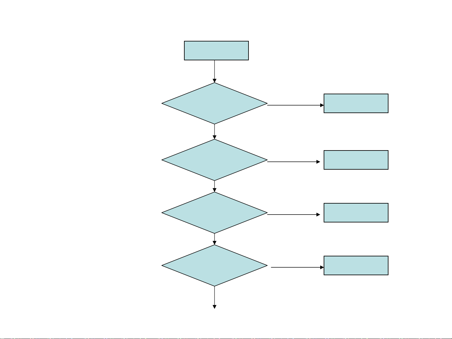
4.20 G sensor inefficacy
G sensor inefficacy
D/L the latest edition,
Check whether it is OK
N
Check whether
U4302 is broken
N
Change the CPU
Y
ok
Y
Change U4302
OK
Page 63

Page 64

 Loading...