

Page 1

MEGA4 Technical Manual
1. Product Specification
2. Mechanical Construction
3. Circuit Description
4. IC Information
5. Spare Part List
6. Map
7. Schematic
8. Block diagram
- COMPANY CONFIDENTIAL -
Ezze Mobile Tech., Inc
Fax.
Tel. +82 (0)2 519 7700
+82 (0)2 519 7882
Page 2

Section 1 – Product Specification
Contents Page
MEGA4 specifications ..……...…………..……………………………………..…… 1.1
Batteries …………………………..………………………………..……………………. 1.3
Standard charger………………………………..…………….………………………… 1.5
- COMPANY CONFIDENTIAL -
Ezze Mobile Tech., Inc
Fax.
Tel. +82 (0)2 519 7700
+82 (0)2 519 7882
Page 3

Section 2 – Mechanical Construction
Contents Page
Disassembly ……………………………………………………………………………... 2.1
Phone disassembly …………………………..……………………………….……… ... 2.2
Phone Assembly ………………………………………………………………………… 2.11
- COMPANY CONFIDENTIAL -
Ezze Mobile Tech., Inc
Fax.
Tel. +82 (0)2 519 7700
+82 (0)2 519 7882
Page 4

Section 3 – Circuit Description
Contents Page
Baseband section …………………………………………………....……… 3.1
I. MT6228 ( GSM/GPRS Baseband processor ) …………..……………….. 3.1
II. MT6318 ( GSM Power Management System ) …………………………... 3.49
III. HYC0UGE0MF1P ( NAND MCP) …………….………………………………..3.62
RF section .............................................................................. 3.67
I. MT6120 ( RF Transceiver IC ) ……………………………………………….… 3.67
II. RF3166 ( QUAD-BAND Power Amplifier Module ) …….……………....3.74
III. LMSP54HA-348TEMP ( Antenna Switch Module for Tri Band ) …. 3.77
- COMPANY CONFIDENTIAL -
Ezze Mobile Tech., Inc
Fax.
Tel. +82 (0)2 519 7700
+82 (0)2 519 7882
Page 5

Section 4 – IC Information
Contents Page
Pin out for U 900 …………………………………………………………...……….….. 4.1
Pin out for U 201 …………………………………………………………...……….…… 4.2
Pin out for BAT 300 …………………………………………………………...……….. 4.3
Pin out for CON 300…………………………………………………………...……….. 4.4
Pin out for CON 380, CON 600 ……………………………………………...……… 4.5
Pin out for U 500 …………………………………………………………...……….… 4.6
Pin out for U 750……………………………………………………...……….………... 4.10
Pin out for U 400……..…………………………………………………...…………..... 4.11
Pin out for LED300~LED305……………………………………………...…...…… 4.12
Pin out for OSC100…………………………………………………………...……….… 4.13
Pin out for U300…………………………………………………….………...……….… 4.14
Pin out for D300,D401,D402………………………………………...………..…….. 4.17
Pin out for U302 …………………………………………………………………………..
4.18
Pin out for U301…………….. ………………………………………………………...……. 4.19
Pin out for ZD390,ZD391,ZD600 …….…………………………………….…….… 4.20
Pin out for ZD601,ZD602,ZD603 …………………………………………………… 4.21
Pin out for U702…………… …………………………………………………………….. 4.22
Pin out for U100……... ………………………………………..………………..…….... 4.23
Pin out for CON450 …….………..………………………………………………….….. 4.33
Pin out for CON750 ………………………………………………………………......... 4.34
Pin out for U200 ……………….…………………………………………………......... 4.35
Pin out for U521 …………………………………..………………………………......... 4.38
Pin out for MIC380 …………………………………………………………………...... 4.39
Pin out for CN90 ………….…...………………………………………………..…….... 4.40
Pin out for U700 ………….…...………………………………………………..…….... 4.41
Pin out for U735 ………….…...………………………………………………..……..... 4.42
Pin out for U600 ………….…...………………………………………………..…….... 4.43
Pin out for LED350 ………….…...………………………………………………..…... 4.44
Pin out for F440 ……………...…...………………………………………………..…... 4.45
- COMPANY CONFIDENTIAL -
Ezze Mobile Tech., Inc
Fax.
Tel. +82 (0)2 519 7700
+82 (0)2 519 7882
Page 6

Section 5 – Spare Part List
Contents Page
MEGA4 Part List ………………………………………………………………………... 5.1
Section 6 – Map
Contents Page
MEGA4 Main Map ………………………………………………….………………... 6.1
MEGA4 Key Map ……………………………………………………………………... 6.5
Section 7 – Schematic
Contents Page
MEGA4 Schematic …………………………………………………...………………... 7.1
Section 8 – Block diagram
Contents Page
MEGA4 Block diagram …………………………………………...…………………... 8.1
- COMPANY CONFIDENTIAL -
Ezze Mobile Tech., Inc
Fax.
Tel. +82 (0)2 519 7700
+82 (0)2 519 7882
Page 7

Model MEGA4 Version V_1.0
Prepared by H/W Date 16/06/2008
Subject Technical Manual Page 1/5
▪ MEGA4 Specifications
General specification Tri Band GSM 900 Class 4, DCS Class 1,
PCS Class 1 handheld cellular telephone
Type approval No. MEGA4
Radiated emissions Complies with I-ETS300020-1
GSM 11.10
Dimensions (mm): Including 750mAh Li-Ion battery
Weight: Including 750mAh Li-Ion battery
Display type Main LCD
Display capacity 240x320 dots,260K color, full graphical
Display icons Soft icons: Signal, Battery, Message
Normal operating temperature
Keyboard Touch panel and 12 keys comprising:
POWER (END), SEND
Ring tones 30 user selectable tones and off
Standard: 96.4x52.4x12 mm
Standard: about 86 grames
2.4 Inch 260K TFT color graphics
display
Vibration, Alarm, Call divert & barring, ,
Broadcast
-20°C to +60°C
2 Soft-Key,(YES/NO)
5 Navigation-Key
Camera, 2Volume(UP/DOWN)
including LED backlight
Battery types Standard:750 mAh Li-Ion
Talk time: 750 mAh Li-Ion battery 4 hours approximately
Standby time: 750 mAh Li-Ion battery
Note²: Measured on DCS1800 with power level 15
200 hours approximately
The talk and standby times are subject to
network conditions
Battery rapid charging time: 750 mAh Li – Ion(standard) 1~1½ hours to >90% of full capacity
Charging Voltage 5.0V
Nominal battery voltage: 750mAh Li - Ion 3.8V
Battery charging CC and CV Mode
Antenna type Internal Antenna
Features supported
(Camera Module) 3.2M Sensor
(Blue Tooth) BT Version 1.2,.
Page 8

Model MEGA4 Version V_1.0
Prepared by H/W Date 16/06/2008
Subject Technical Manual Page 2/5
-. 9 Profiles
(subject to network implementation) 16X16,10X12,8X8 Numeral display
External interface connections RS232, USB
Number of channels GSM900 : 124 channels
DCS1800 : 374 channels.
PCS1900 : 299 channels
Operating Frequency Range GSM900 TX : 880~915Mhz
GSM900 RX : 925~960Mhz
DCS1800 TX : 1710~1785Mhz
DCS1800 RX : 1805~1880Mhz
PCS1900 TX : 1900~1910Mhz
PCS1900 RX : 1930~1990Mhz
HSP, HFP, GAVDP, A2DP,AVRCP,
FTP, OPP, DUN, SPP
8x8,10x10,11x11,12x12,13x14 Roman
display
Support Phase 2 plus Feature
64 Poly stereo sounds
Graphics and animated icons
Phone memory location (200
numbers)
Dynamic text display
Easy text input (Tegic 9)
SIM application tool kit
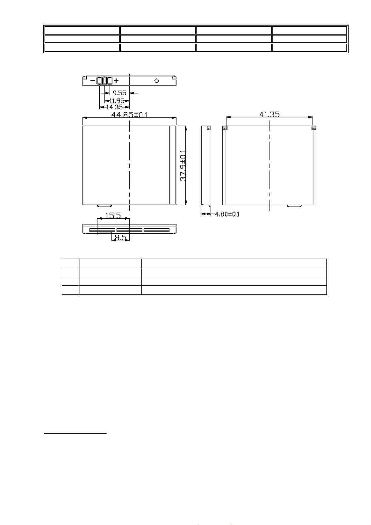
▪ Battery
Page 9
Model MEGA4 Version V_1.0
Prepared by H/W Date 16/06/2008
Subject Technical Manual Page 3/5
①② ③
Function Description
1 VBat Battery Supply Pin
2 Battery ID Battery ID Resistor Pin 10Kohm
3 GND GND
Standard Battery 750mAh Li-Ion
Type: Lithium Ion Rechargeable Battery
Capacity 25°C: 750mAh
Standby time: up to 200 hours.
Talk time (1900MHZ): 30dBm: 2.5 hours 4 hours*
Charging time: 1½-2 hours approximately to full capacity.
Charge temperature: 0 to +45°C.
Discharge temperature: -20 °C to +60°C.
Cycle life 100% cap. to 80% cap. 500 cycles.
Energy Density 344Wh/I 150Wh/kg
Dimension (W x H x L): 4.80 T x 37.90 W x 44.85 L mm.
Weight: about 17g .
*Operating times depend on network and usage. Variability will occur. DTX +40% (included).
Storage temperature:
Short period <1 month: -20°C to +45°C.
Long period <1 year: -20°C to +25°C.
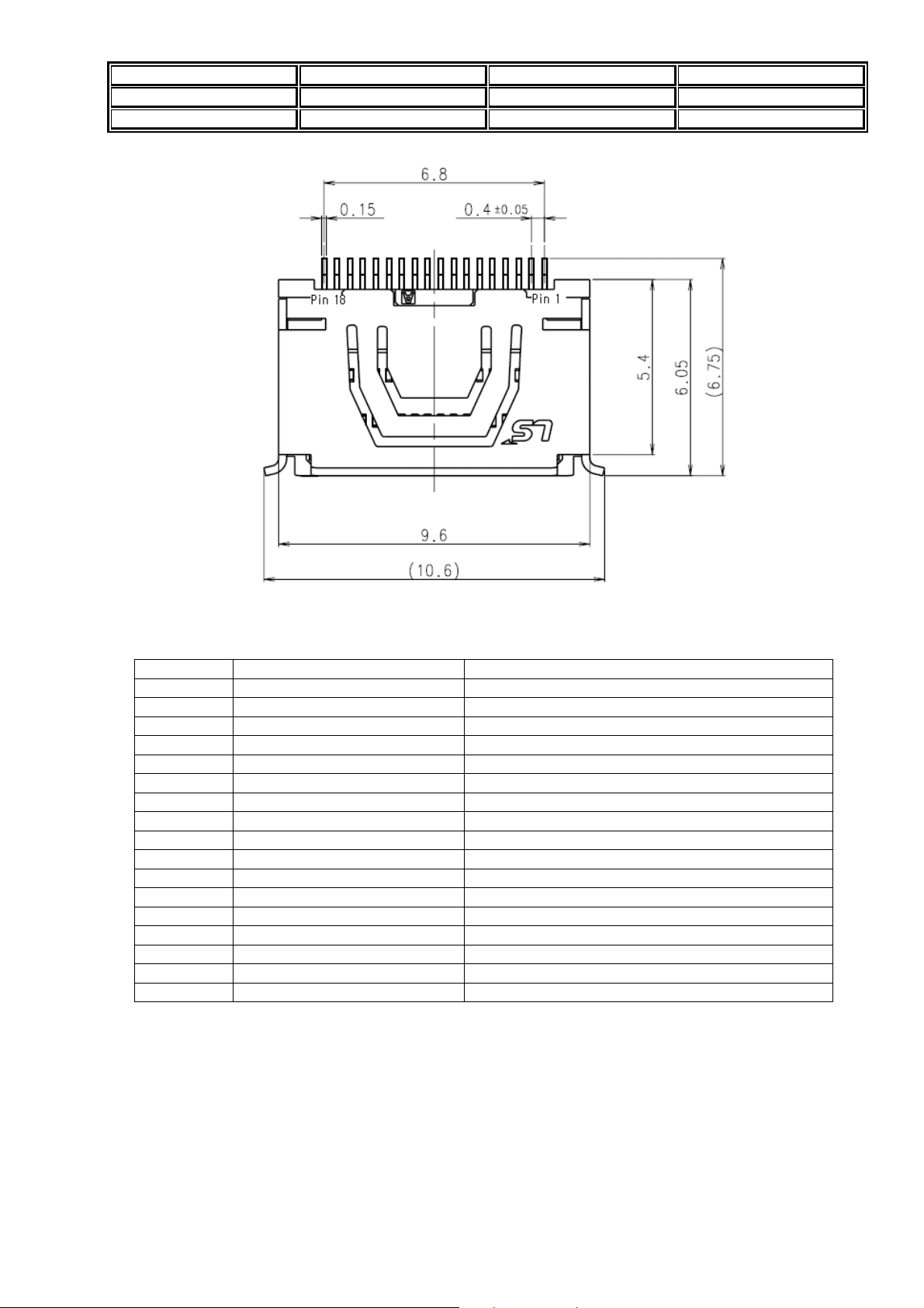
▪ I/O Connector layout : 18pin
Page 10
Model MEGA4 Version V_1.0
Prepared by H/W Date 16/06/2008
Subject Technical Manual Page 4/5
Pin description
Pin 1
2
3
4
5
6
7
8
9
10
11
12
13
14
15
16
17
18
EJ_Out_L Headset Receiver Left
EJ_Out_R Headset Receiver Right
GND GND
EJ_Mic Headset Mic Input
GND GND
EJ_GND Headset GND
NC NC
Headset Interrupt Headset Interrupt
Power_On_Off Power On Off
USB_DM USB D+ input / Output
USB_DP USB D- input / Output
RXD UART RX
TXD UART TX
Charger/USB Power USB Power / Charger
Charger/USB Power USB Power / Charger
NC Not connected
VBAT Battery Voltage +3.8V
VBAT Battery Voltage +3.8V
Standard charger
MEGA4 is supplied with a SMTP charger as standard. The charger is connected to the Power
management IC through the bottom port.
Page 11

Model MEGA4 Version V_1.0
Prepared by H/W Date 16/06/2008
Subject Technical Manual Page 5/5
Charging of the battery can only be carried out when the battery is fitted to the phone. There are no
serviceable parts within the main plug.
Input parameter Type Value Unit
Input voltage min 90 V
nom 230 V
max 264 V
Input frequency min 47 Hz
nom 50 Hz
max 63 Hz
Input current max 200 mA
Efficiency min >55 %
Output parameter Type Value Unit
Output current(CV) min 0.650 A
max 0.800 A
(CC) min 0.000 A
max 0.650 A
Output voltage(CV) min 3.0 V
max 4.9 V
(CC) min 4.9 V
max 5.3 V
Connector 18pin Bottom Connector
Cable length 1.5 m.
Page 12

Model MEGA4 Version V_
Prepared by H/W Date 2008.05.20
Subject Technical Manual Page 1/21
Disassembly
This section covers the assembly and disassembly for MEGA4 phone. In order to carry out the
assembly or disassembly the following precautions should be taken:
1. A Plus screwdriver is required to remove the screw which holds the two casings together.
Ensure that the screwdriver is narrow enough to reach the screws without causing damage to
the casing parts.
2. The phone should always be placed on a soft surface to minimise the risk of damage being
caused to the casing, window and keypad. If the PCB is to be removed, then care should be
taken not to stress or scratch the exposed LCD and touch window.
3. Observe anti-static precautions when handling the main PCB or any of its components.
4. Repairs carried out by unauthorised persons will result in the warranty on the unit becoming
void.
5. Do not use solvents to clean any of the casing parts or the LCD window.
Page 13
Model MEGA4 Version V_
Prepared by H/W Date 2008.05.20
Subject Technical Manual Page 2/21
Phone disassembly
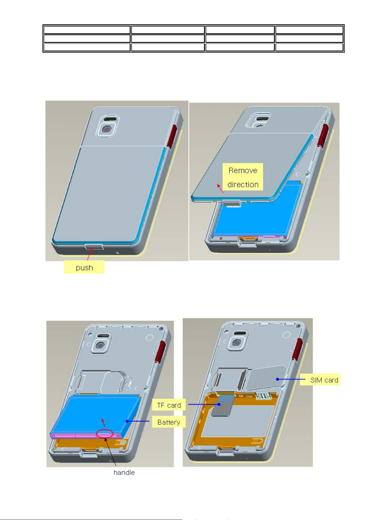
1. Battery Cover Disassembly
A. Push the Lock and remove battery cover along the remove direction.
2. Battery & SIM card & TF card Disassembly
A. Hold the handle of the battery and remove it along the arrow direction
B. Remove SIM card
C. Remove TF card
Page 14
Model MEGA4 Version V_
Prepared by H/W Date 2008.05.20
Subject Technical Manual Page 3/21
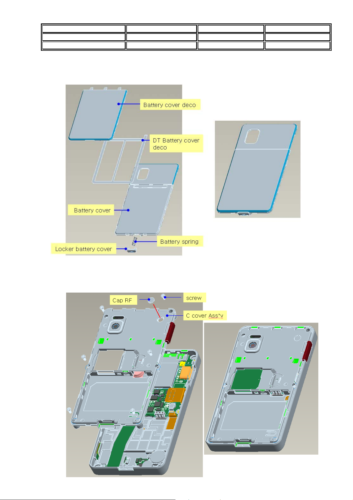
3. Battery cover Sub Ass’y Disassembly
A. Refer to the explode view. Can not remove as bellow after join them
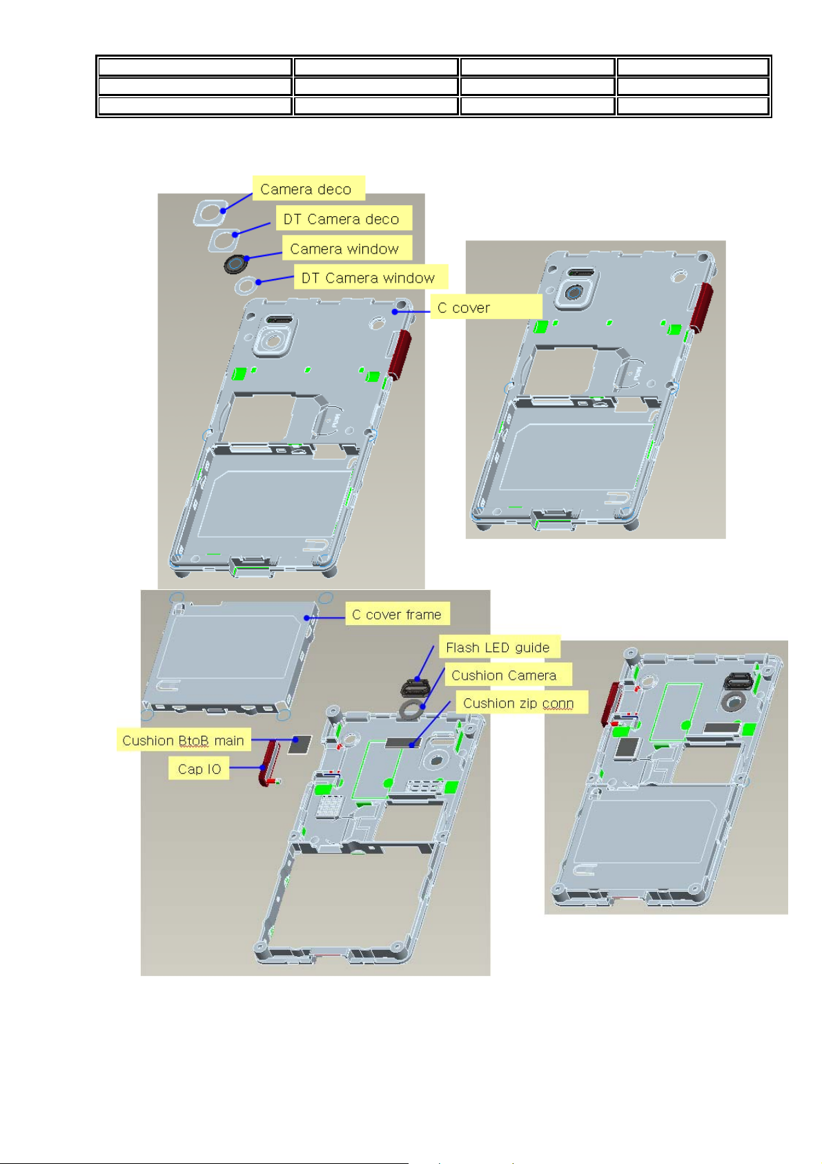
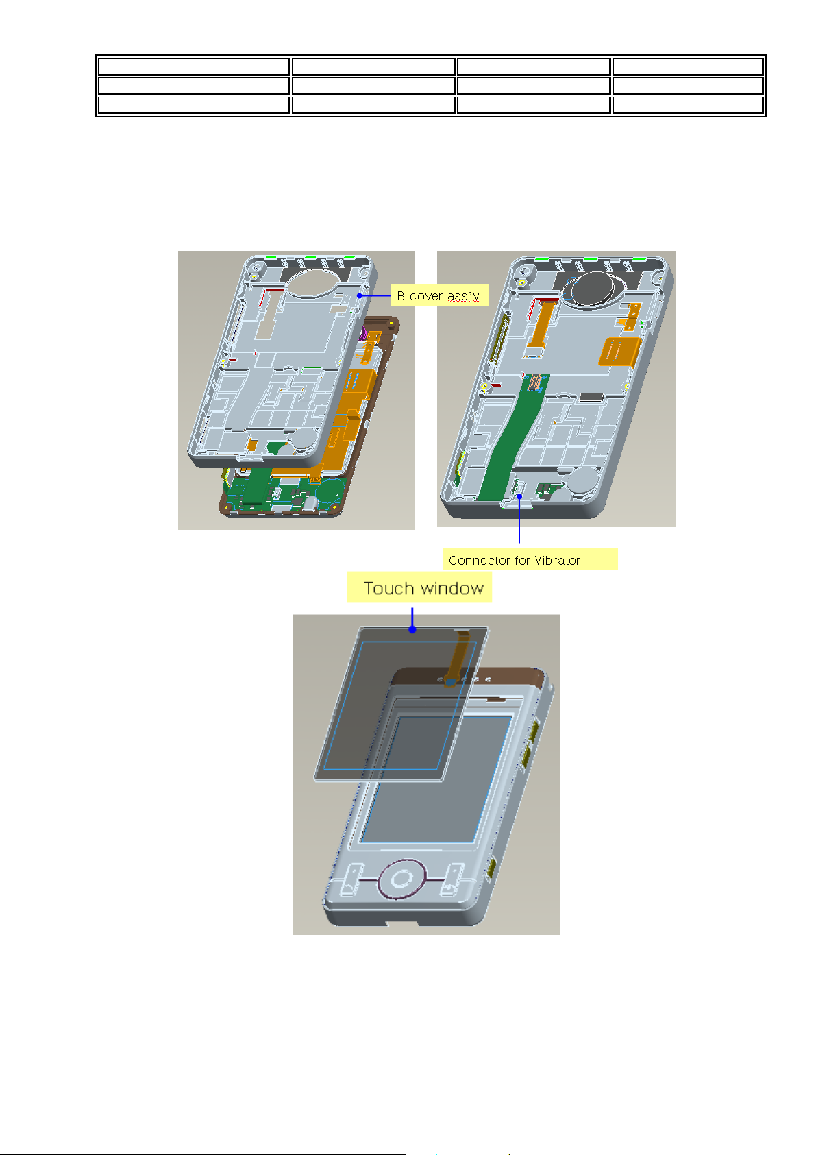
4. C cover Disassembly
A. Remove RF cap and six of screws. Carefully separate two covers
(C cover Ass’y and B cover)
Page 15
Model MEGA4 Version V_
Prepared by H/W Date 2008.05.20
Subject Technical Manual Page 4/21
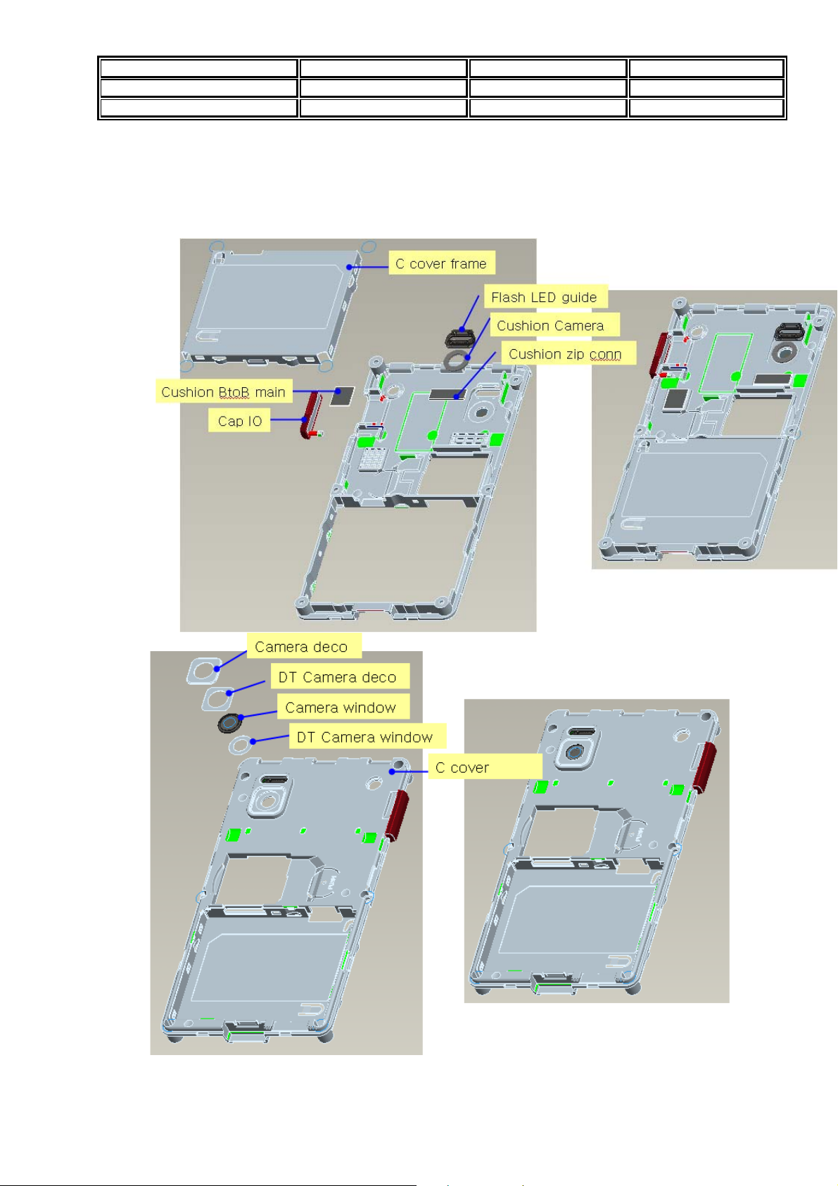
5. C cover Sub Ass’y Disassembly
A. Refer to the explode view as bellow.
6. PCB ASS’Y & B cover Disassembly
Page 16
Model MEGA4 Version V_
Prepared by H/W Date 2008.05.20
Subject Technical Manual Page 5/21
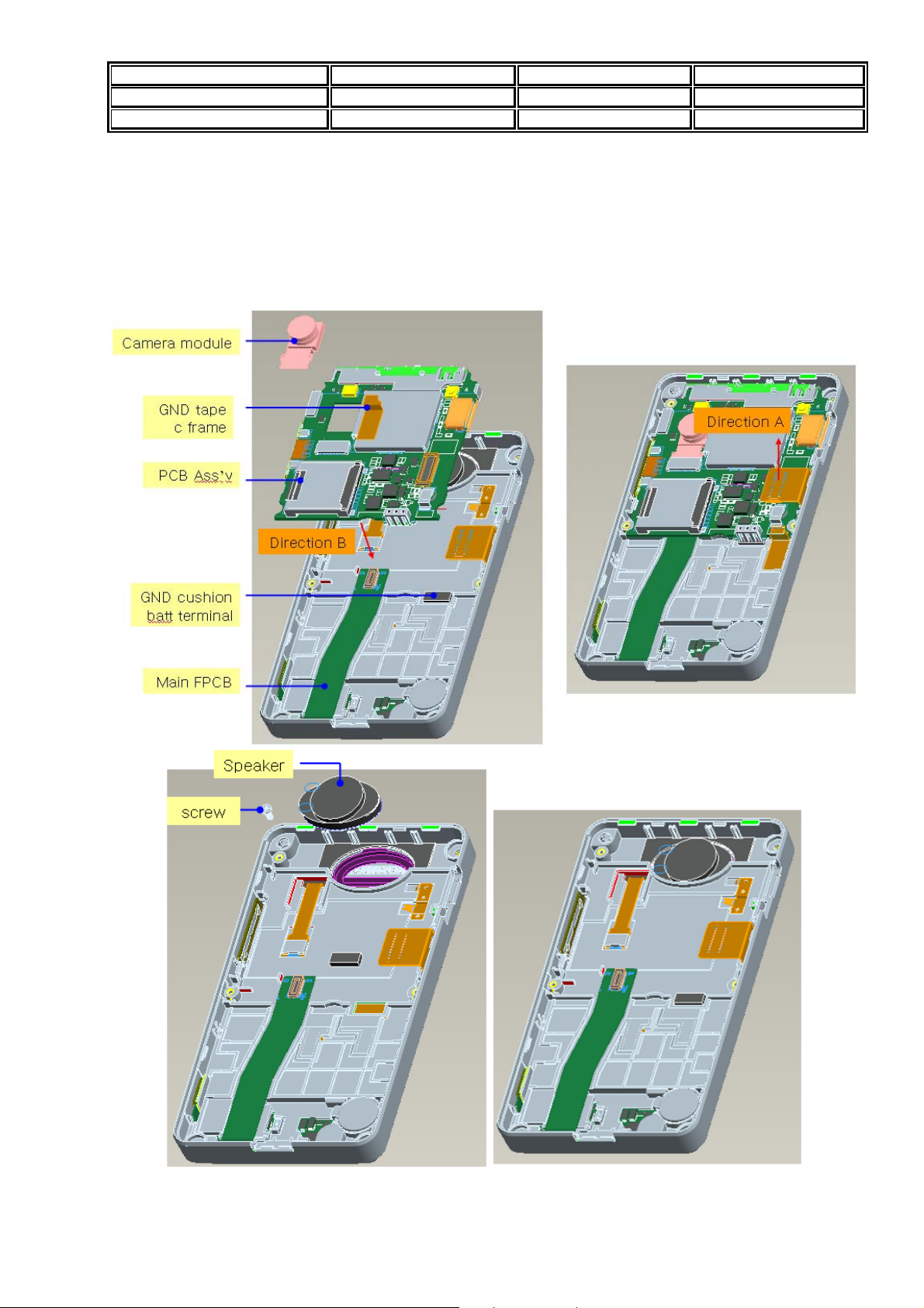
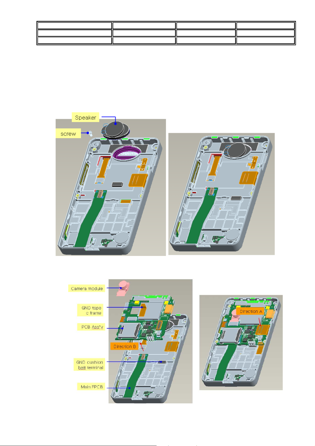
A. unconnect the LCD FPCB along the direction A as right view
B. Remove the camera module
C. Remove the PCB Ass’y
D. Unconnect the main FPCB along the direction B
E. Remove a screw
F. Remove a speaker
7. PCB Disassembly
Page 17
Model MEGA4 Version V_
Prepared by H/W Date 2008.05.20
Subject Technical Manual Page 6/21
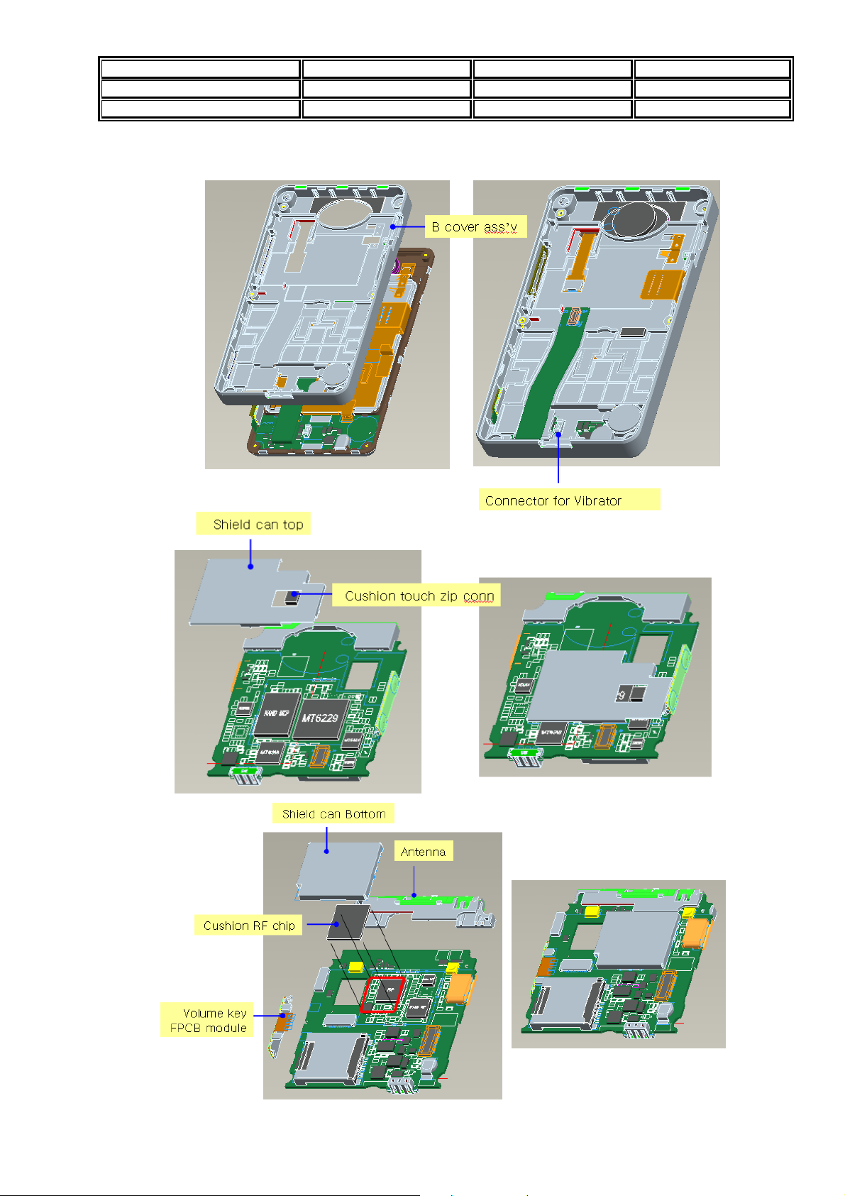
A. unconnect the vibrator
B. Remove the B cover Ass’y
8. B cover Sub Ass’y Disassembly
Page 18
Model MEGA4 Version V_
Prepared by H/W Date 2008.05.20
Subject Technical Manual Page 7/21
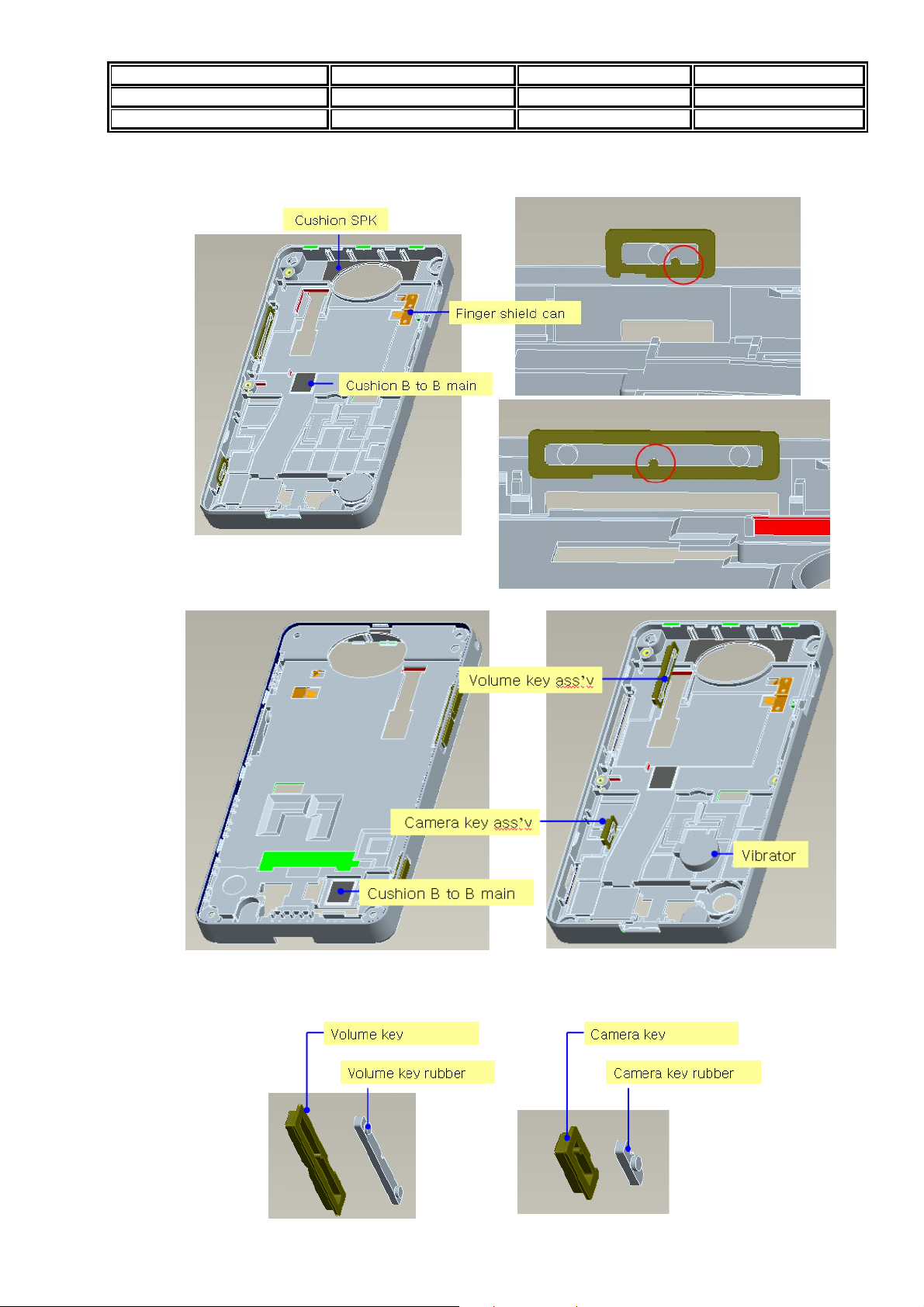
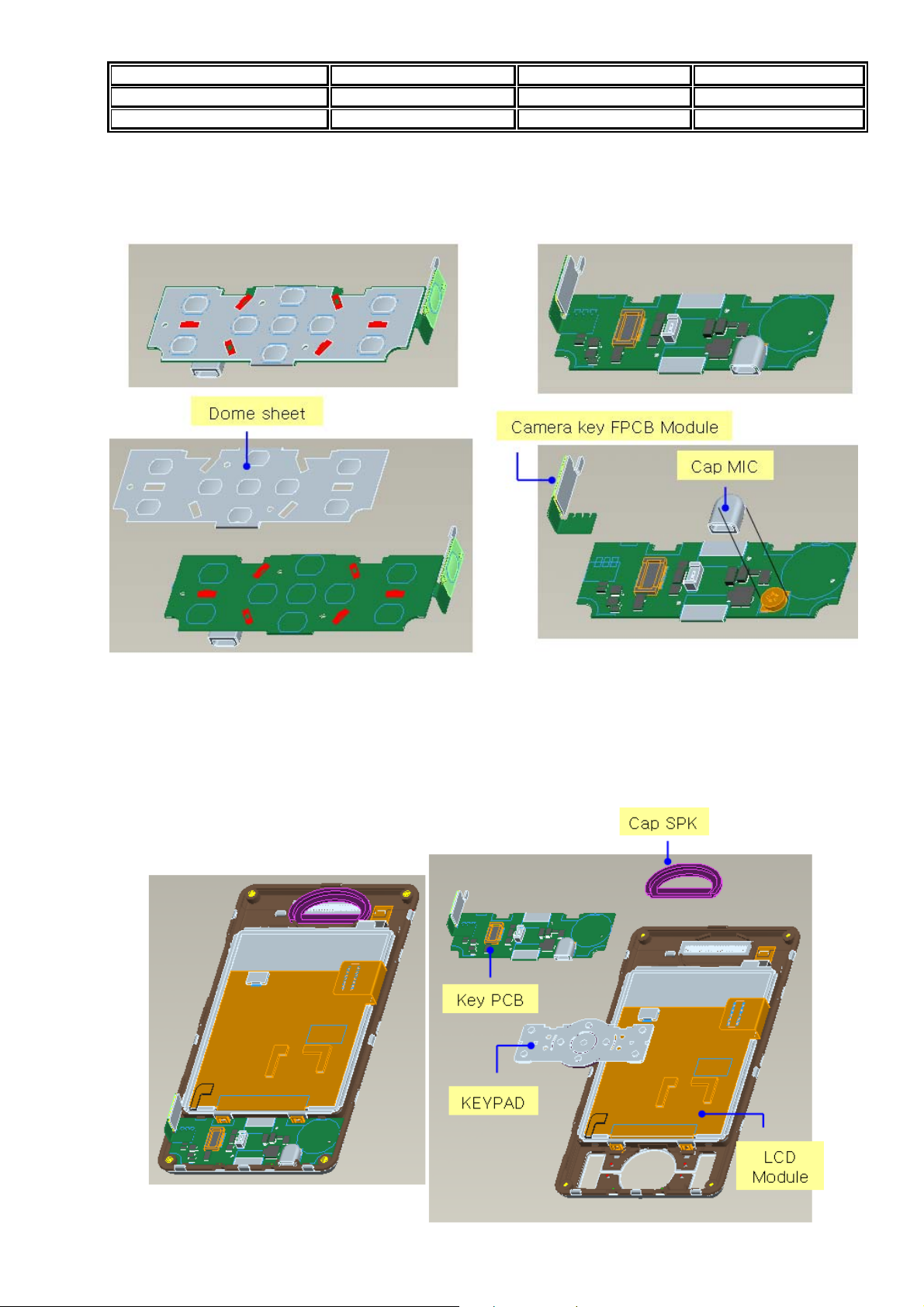
A. Remove the volume key ass’y & camera key ass’y
B. Remove the volume key rubber and camera key rubber
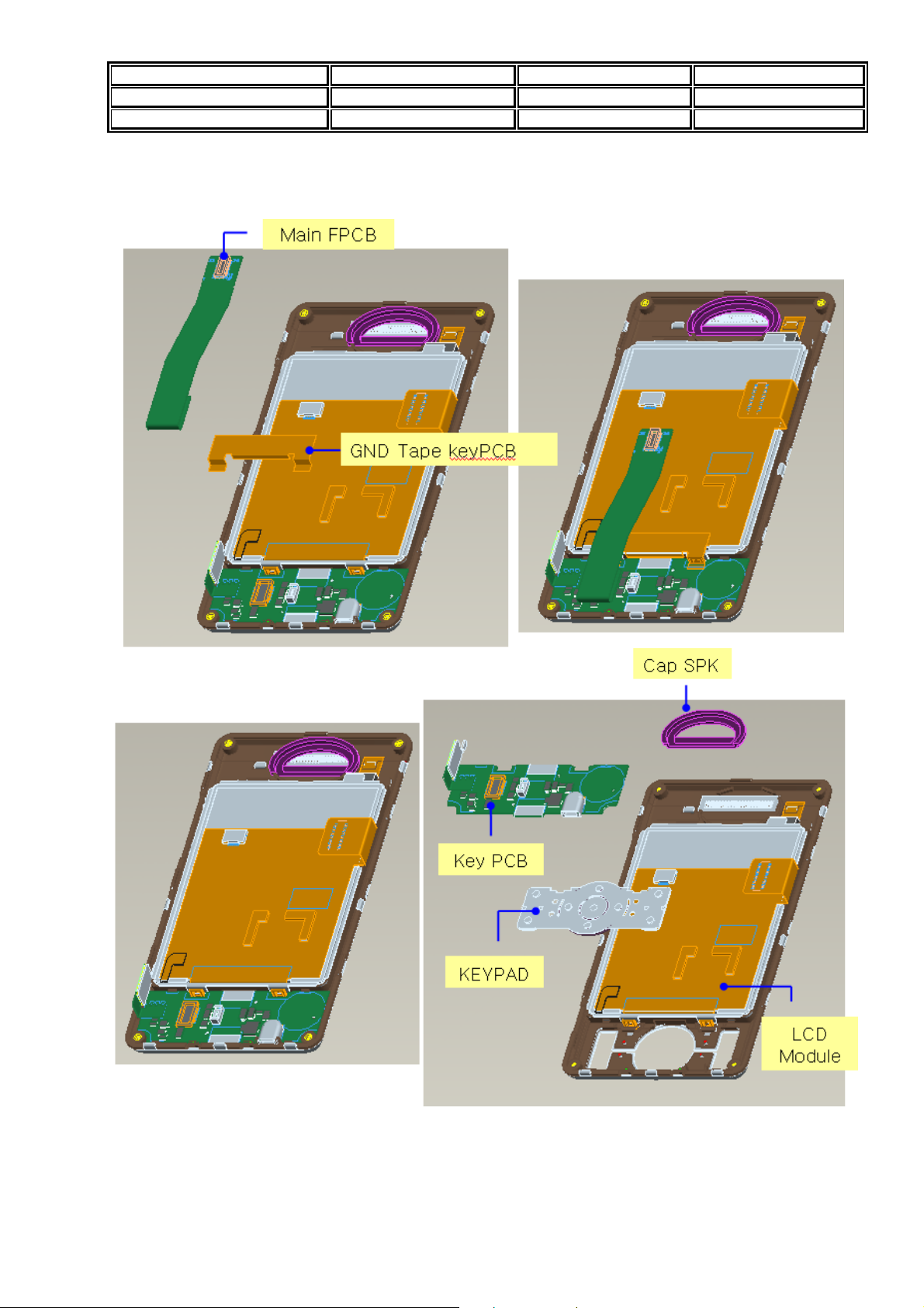
9. A cover & Key PCB & LCD Disassembly
Page 19
Model MEGA4 Version V_
Prepared by H/W Date 2008.05.20
Subject Technical Manual Page 8/21
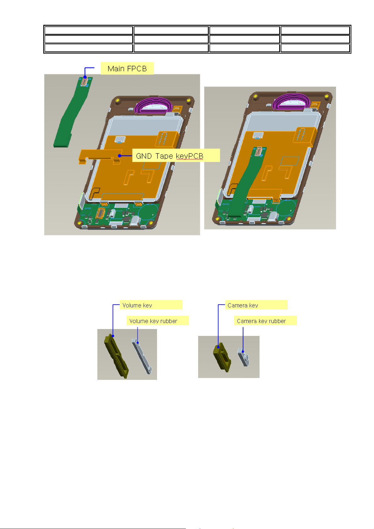
A. Remove the main FPCB.
B. Remove the GND tape key PCB
C. Remove LCD module
10. KeyPCB Disassembly
Page 20
Model MEGA4 Version V_
Prepared by H/W Date 2008.05.20
Subject Technical Manual Page 9/21
A. Remove Cap MIC.
11. A cover Sub Ass’y Disassembly
Page 21
Model MEGA4 Version V_
Prepared by H/W Date 2008.05.20
Subject Technical Manual Page 10/21
Page 22
Model MEGA4 Version V_
Prepared by H/W Date 2008.05.20
Subject Technical Manual Page 11/21
Phone Assembly
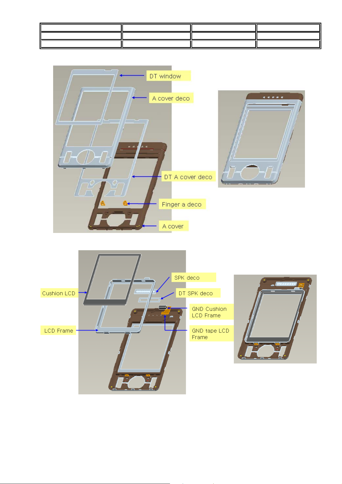
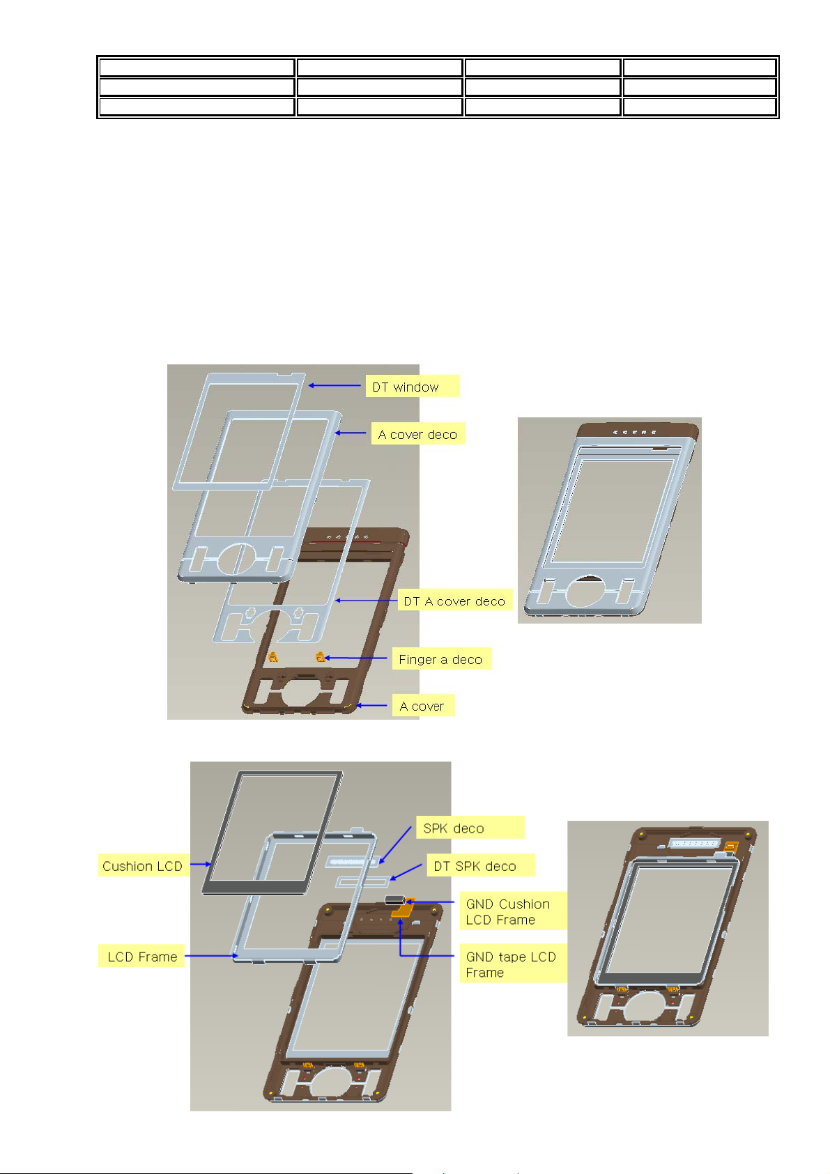
1. A cover Sub Ass’y assembly
A. Put the 2 of “finger a deco” in the a cover
B. Attach the “dt a cover deco” on the a cover
C. Join the “a cover” deco with “a cover”
D. Attach the “ dt spk deco” & “spk deco” in side of a cover
E. Attach the “GND tape LCD frame” at the right finger of a cover deco
F. Attach the “GND cushion LCD frame” on the “GND tape LCD frame”
G. Put the “LCD frame” in the hole of “A cover”
H. Attach the “cushion LCD” in the “LCD frame”
Page 23
Model MEGA4 Version V_
Prepared by H/W Date 2008.05.20
Subject Technical Manual Page 12/21
2. Key PCB assembly
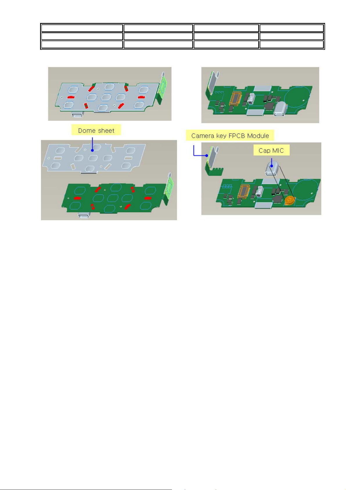
A. Solder the “camera FPCB module” on the rear side of the “KeyPCB”.
B. Attach the “dome sheet” on the front side of the “ keyPCB”
C. Put the “cap MIC” on the out side of the MIC
3. A cover ASS’Y & LCD & KeyPCB assembly
A. Put the “keypad” in the “a cover”.
B. Put the “KeyPCB” in the “a cover”.
C. Connect “Main FPCB” with connector on the rear side of the “key PCB”
D. Put the “LCD module” in the “a cover”
E. Put the “Cap SPK” in the “a cover”
F. Attach the “GND tape keyPCB” inside of the silk line on the “LCD” and “KeyPCB”
Page 24
Model MEGA4 Version V_
Prepared by H/W Date 2008.05.20
Subject Technical Manual Page 13/21
4. B cover Sub Ass’y assembly
A. Put the “volume key rubber” in the “volume key”.
B. Put the “camera key rubber” in the “camera key”.
Page 25
Model MEGA4 Version V_
Prepared by H/W Date 2008.05.20
Subject Technical Manual Page 14/21
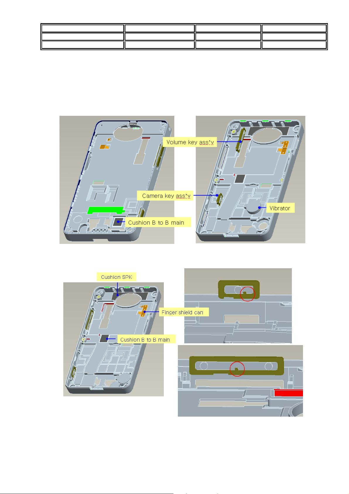
C. Put the “finger shield can” in the pole and Hot melt.
D. Attach the “cushion btob main” on the front side and rear side.
E. Attach the “cushion spk”
F. Put the “volume key” and “camera key” in the each hole
---- attention insertion direction
G. Attach the vibrator
Page 26
Model MEGA4 Version V_
Prepared by H/W Date 2008.05.20
Subject Technical Manual Page 15/21
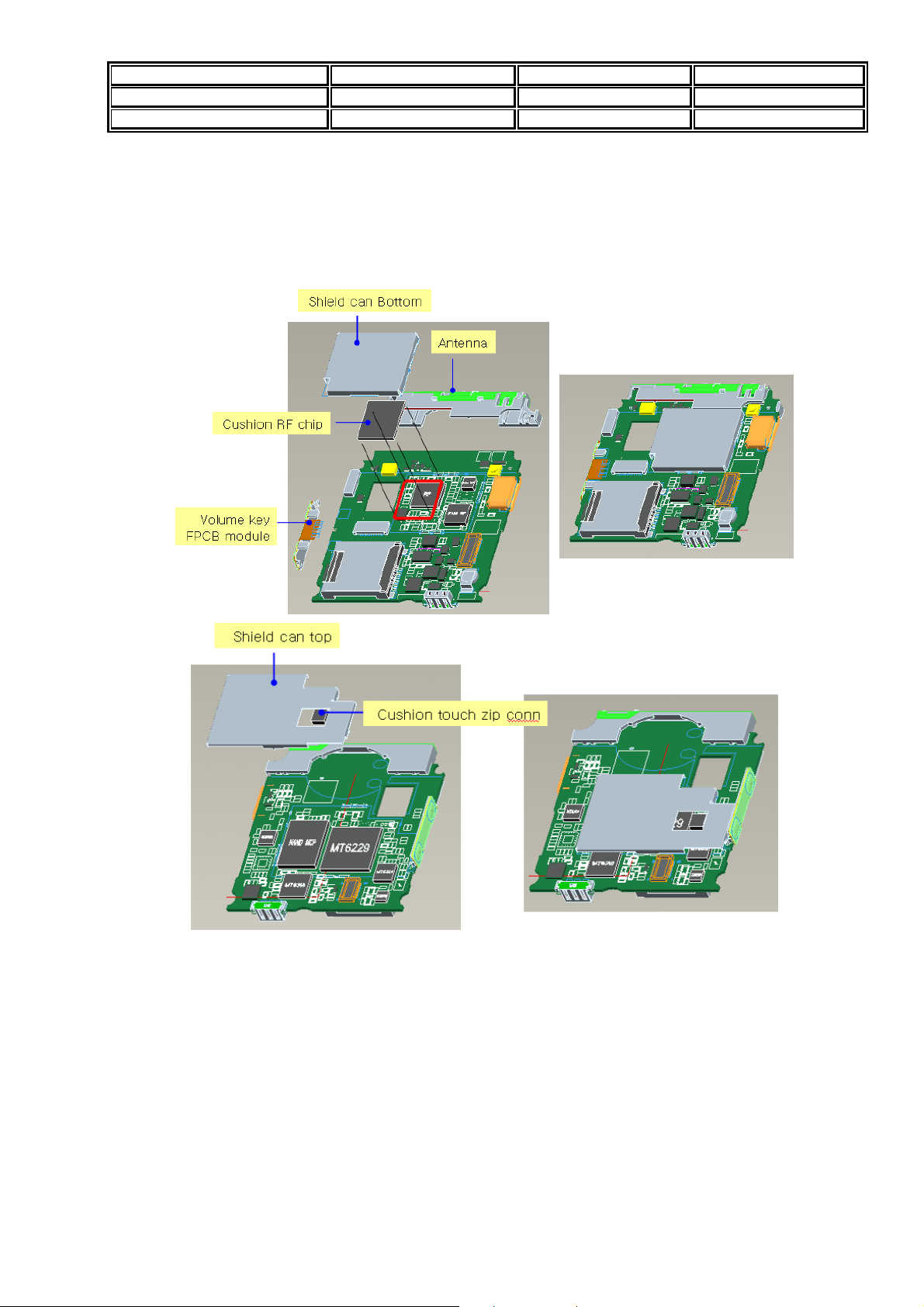
5. PCB ASS’Y Assembly
A. Solder the “volume key FPCB module”
B. Attach the “cushion RF chip”
C. Insert 2 of shield can on the front and rear side
D. Attach the “cushion touch zip conn”
E. Insert antenna
Page 27
Model MEGA4 Version V_
Prepared by H/W Date 2008.05.20
Subject Technical Manual Page 16/21
6. B cover assembly
A. Join the “b cover” with “A cover”
B. Connect vibrator with connector
C. Connect “ Touch window” with connector
Page 28
Model MEGA4 Version V_
Prepared by H/W Date 2008.05.20
Subject Technical Manual Page 17/21
7. PCB assembly
A. Drive a screw
B. Insert speaker
C. Attach the “GND cushion batt terminal”
D. Connect PCB with main FPCB along the direction B
E. Join the PCB with B cover
F. Connect LCD connector with PCB along the direction A
G. Connect Camera module with zip connector and insert to hole
Page 29
Model MEGA4 Version V_
Prepared by H/W Date 2008.05.20
Subject Technical Manual Page 18/21
8. C cover SUB Ass’y assembly
A. Insert “flash LED guide” in the 4 of poles and hot melt 4 of poles
B. Attach the almost parts as bellow
C. Join the “C cover frame” with C cove
9. C cover ASS’Y Assembly
Page 30
Model MEGA4 Version V_
Prepared by H/W Date 2008.05.20
Subject Technical Manual Page 19/21
A. Join the C cover assy with B cover
B. Drive 6 of screws
C. Attach the “cap rf”
10. Battery cover SUB Ass’y assembly
A. Insert “battery spring” to “Locker battery cover” and join them with “Battery cover”
B. Attach the “DT batter cover deco” on the “battery cover”
C. Join the “battery cover deco” with “battery cover” and hot melt 3 of poles
11. SIM Card & TF card & Battery assembly
Page 31

Model MEGA4 Version V_
Prepared by H/W Date 2008.05.20
Subject Technical Manual Page 20/21
A. Insert SIM card and TF card as bellow
B. Insert battery under the hook as bellow and put it down to arrow direction
12. SIM & TF card & Battery Assembly
A. Insert battery cover under the hook and put it down to arrow direction and push as
bellow
13. Protect tape assembly
Page 32

Model MEGA4 Version V_
Prepared by H/W Date 2008.05.20
Subject Technical Manual Page 21/21
Page 33

MODEL MEGA4 VERSION V_1.00
PREPARED BY H/W DATE 29/05/2008
SUBJECT TECHNICAL MANUAL PAGE 1/79
Baseband section
This document provides a description of the baseband section of the MEGA4. Most design decisions are explained,
but no detailed calculations are included. Total chip solutions(MT6228, MT6318, MT6120) except for RF Power
Amplifier(RF3166) are from Media Tek, Taiwan.
I. MT6228 ( GSM/GPRS Baseband Processor )
1. System Over View
The Revolutionary MT6228 is a leading edge single-Chip solution for GSM/GPRS mobile phones targeting the emerging
TM
applications in digital audio and video. Based on 32bit ARM7EJ-S
performance GPRS Class 12 MODEM, but also provides comprehensive and advanced solutions for handheld multimedia. But, the MEGA4 just supports GPRS Multi-slot Class 8 and GPRS MODE CLASS B.
The Figure 1 is shown Typical Application for MT6228.
RISC processor, MT6228 not only features high
1.1 Platform Feature
Figure 1 : Typical Application for MT6228
Page 34

MODEL MEGA4 VERSION V_1.00
PREPARED BY H/W DATE 29/05/2008
SUBJECT TECHNICAL MANUAL PAGE 2/79
z General
-. Integrated voice-band, audio-band and base-band analog front ends.
-. TFBGA 13mm x 13mm, 314balls, 0.65mm pitch package.
z MCU Subsystem
-. ARM7EJ-S 32bit RISC processor
-. High Performance Multi-layer AMBA bus
-. Java hardware acceleration for fast Java-based games and applets.
-.Operating frequency : 25/52/104Mhz
-. Dedicated DMA Bus
-. 14 DMA channels
-. 1M bits on-chip SRAM
-. 1M bits MCU dedicated Tightly Coupled memory
-. 256K bits CODE cache
-. 64K bits DATA cache
-. On-chip boot ROM for factory flash programming
-. Watchdog timer for system crash recovery
-. 3sets of General purpose timer
-. Circuit Switch Data coprocessor
-. Division coprocessor
-. PPP Framer coprocessor
z External Memory Interface
-. Supports up to 4 external devices
-. Supports 8-bit or 16-bit memory components with maximum size of up to 64M bytes each.
-. Supports Mobile RAM and Cellular RAM
-. Supports Flash and SRAM/PSRAM with page mode or burst mode
-. Industry standard Parallel LCD interface
-. Supports Multi-media companion chips with 8/16bits data width.
-. Flexible I/O voltage of 1.8V ~ 2.8V for memory interface.
z User Interface
-. 6-row x 7-column keypad controller with hardware scanner.
-. Supports multiple key presses for gaming.
-. SIM/USIM controller with hardware T=0/T=1 protocol control.
-. Real Time Clock(RTC) operating with a separate power supply.
-. General Purpose I/Os (GPIOs)
-. 2sets of Pulse Width Modulation(PWM) output.
-. Alerter Output with enhanced PWM or PDM.
-. 8 external interrupt lines.
z Security
-. Cipher : supports AES, DES/3DES
Page 35

MODEL MEGA4 VERSION V_1.00
PREPARED BY H/W DATE 29/05/2008
SUBJECT TECHNICAL MANUAL PAGE 3/79
-. Hash : Supports MD5, SHA-1
-. Supports security key and 2kit chip unique ID
z Connectivity
-. 3 UARTs with hardware flow control and speed up to 921600pbs.
-. IrDA modulator/Demodulator with hardware framer. Supports SIR/MIR/FIR operating Speeds.
-. Full speed USB 1.1 OTG capability. Support Device mode, limited host mode and dual-role OTG mode.
-. Multi Media Card, Secure Digital Memory Card, Memory Stick, Memory Stick Pro Host Controller with flexible
I/O Voltage power.
-. Supports SDIO interface for SDIO peripherals as well as WIFI connectivity.
-. DAI/PCM and I2S interface for Audio application.
z Power Management
-. Power Down Mode for analog and digital circuits.
-. Procesor Sleep Mode
-. Pause Mode of 32Khz clocking in Standby state
-. 7 channel Auxiliary 10bit A/D converter for charger and battery monitoring and photo sensing.
z Test and Debug
-. Built-in digital and analog loop back modes for both Audio and baseband front-end.
-. DAI port complying with GSM Rec.11.10
-. JTAG port for debugging embedded MCU.
1.2 Model Feature
z Radio Interface and Baseband Front End
-. GMSK Modulator with analog I and Q channel outputs.
-. 10-bit D/A convert for Uplink baseband I and Q signals.
-. 14bit high resolution A/D converter for downlink baseband I and Q signals.
-. Calibration mechanism of offset and gain mismatch for baseband A/D converter and D/A converter.
-. 10bit D/A converter for Automatic Power Control(APC)
-. 13bit high resolution D/A converter for Automatic frequency Control(AFC)
-. Programmable Radio RX filter.
-. 2 channels Baseband Serial Interface(BSI) with 3-wire control.
-. Bi-Directional BSI interface. RF chip register read access with 3-wire or 4-wire interface
-. 10 pin Baseband Parallel Interface(BPI) with programmable driving strength.
-.Multi-band Support (GSM900, GSM900, DCS1800, PCS1900)
z Voice and Model Codec
-. Dial tone Generation.
-. Voice memo
-. Noise reduction
-. Echo suppression
-. Advanced sidetone Oscillation Reduction.
-. Digital sidetone generator with programmable gain.
Page 36

MODEL MEGA4 VERSION V_1.00
PREPARED BY H/W DATE 29/05/2008
SUBJECT TECHNICAL MANUAL PAGE 4/79
-.Two programmable acoustic compensation filters.
-. GSM/GPRS quad vocoders for adaptive multirate(AMR), enhanced full rate(EFR), full rate(FR) and half rate(HR).
-. GSM channel coding, equalization and A5/1 and A5/2 ciphering.
-.GPRS GEA1 and GEA2 ciphering.
-. Programmable GSM/GPRS model.
-. Packet Switched data with CS1/CS2/CS3/CS4 coding schemes.
-.GSM circuit switch data.
-. GPRS Class 12.
z Voice Interface and Voice Front End.
-. Two microphone inputs sharing one low noise amplifier with programmable gain and automatic gain control(AGC)
mechanisms.
-. Voice power amplifier with programmable gain.
-. 2’nd order Sigma-Delta A/D converter for voice uplink path.
-. D/A Converter for Voice downlink path.
-. Supports Half-duplex hands-free operation.
-. Compliant with GSM 03.50.
1.3 Multimedia Feature
z LCD/NAND Flash Interface
-. Dedicated Parallel Interface supports 3 external devices with 8/16 bits NAND flash interface, 8/9/16/18 bit Parallel
interface and serial interface for LCM.
-. Built-in NAND flash controller with 1 bit ECC for mass storage.
z LCD Controller
-. Supports simultaneous connection to up to 3 parallel LCD and 2 serial LCD modules.
-. Supports LCM format : RGB332, RGB444, RGB565, RGB666, RGB888.
-. Supports LCD Module with maximum resolution up to 800x600 at 24bpp.
-. Per pixel alpha channel.
-. True colour engine
-. Supports hardware display rotation.
-. Capable of combining display memories with up to 6 blending layers.
z Image Signal Processor
-. 8/10 bit Bayer format image input.
-. YUV422 format image input.
-. Capable of processing image of size up to 3M pixels.
-. Colour correction matrix.
-. Gamma correction.
-. Automatic exposure(AE) control.
-. Automatic focus control.
-. Automatic white balance(AWB) control.
-. Programmable AE/AEB windows.
Page 37

MODEL MEGA4 VERSION V_1.00
PREPARED BY H/W DATE 29/05/2008
SUBJECT TECHNICAL MANUAL PAGE 5/79
-. Edge enhancement support.
-. Shading compensation.
-. Defect Pixel compensation.
z Graphic Compression.
-. GIF decoder, PNG Decoder.
z JPEG Decoder
-. ISO/IEC 10918-1 JPEG Baseline and Progressive modes.
-. Supports all possible YUV formats, Including gray scale format.
-. Supports all DC/AC Huffman table parsing.
-. Supports all quantization table parsing.
-. Supports a restart interval
-. Supports SOS, DHT, DQT and DRI marker parsing.
-. IEEE Std 1180-1990 IDCT standards compliance
-. Supports progressive image processing to minimize storage space requirement.
-. Supports reload-able DMA for VLD stream.
z JPEG Encoder
-. ISO/IEC 10918-1 JPEG baseline mode.
-.ISO/IEC 10918-2 compliance
-. Supports YUV422 and YUV420 and grayscale formats.
-. Supports JFIF.
-. Standard DC and AC Huffman tables.
-. Provides 4 levels of encode quality.
-. Supports continuous shooting.
z Image Data Processing.
-. Supports Digital Zoom.
-. Supports RGB888/565, YUV444 image processing.
-. High throughput hardware scaler. Capable of tailoring an image to an arbitrary size.
-. Horizontal scaling in averaging method.
-. Vertical scaling in bilinear method.
-. Simultaneous scaling for MPEG-4 encode and LCD display.
-. YUV and RGB color space conversion.
-. Pixel format transform.
-. Boundary padding.
-. Pixel processing : hue/saturation/intensity/color adjustment, Gamma correction and grayscale/invert/sepia-tone effects.
-. Programmable spatial filtering : linear filter, non-linear filter and multi-pass artistic effects.
-. Hardware accelerated image editing.
-. Photo frame capability.
-. RGB thumbnail data output.
z MPEG-4/H.263 CODEC
Page 38

MODEL MEGA4 VERSION V_1.00
PREPARED BY H/W DATE 29/05/2008
SUBJECT TECHNICAL MANUAL PAGE 6/79
-. Hardware Video CODEC.
-. ISO/IEC 14496-2 simple profile :
Decode @ level 0/1/2/3
Encode @ level 0.
-. ITU-T H.263 profile 0 @level 10.
-. Max decode speed is VGA @15fps.
-. Max encode speed is CIF@15fps.
-. Support VGA mode encoding.
-. Horizontal and vertical de-blocking filter in video playback.
-. Encoder resync marker and HEC.
-. Support visual tools for decoder : I-VOP, P-VOP, AC/DC Prediction, 4-MV, Unrestricted MV, Error Resilience, Short
Header.
-. Error Resilience for decoder : Slice Re-synchronization, Data Partitioning, Reversible VLC.
-. Supported visual tools for encoder : I-VOP, P-VOP, Half-Pel, DC Prediction, Unrestricted MV, Reverible VLC, Short
Header.
-. Supports encoding motion vector of range up to -64/+63.5 pixels.
-. HE-AAC decode support.
-. AAC/AMR/WB-AMR audio decode support
-. AMR/WB-AMR audio encode support.
z TV-OUT
-. Supports NTSC/PAL formats(interlaced mode)
-. 10bit video DAC with 2x over sampling.
-. Supports one composite video output.
z Audio CODEC
-. Supports HE-AAC codec decode
-. Supports AAC codec decode
-. Wavetable synthesis with up to 64 tones
-. Advanced wavetable synthesizer capable of generating simulated stereo
-. Wavetable including GM full set of 128 instruments and 47 sets of percussions
-. PCM Playback and Record
-. Digital Audio Playback
z Audio Interface and Audio Front End
-. Supports I2S interface
-. High resolution D/A Converters for Stereo Audio playback
-. Stereo analog input for stereo audio source
-. Analog multiplexer for stereo audio
-. Stereo to mono conversion
Page 39

MODEL MEGA4 VERSION V_1.00
PREPARED BY H/W DATE 29/05/2008
SUBJECT TECHNICAL MANUAL PAGE 7/79
Figure 2 is shown the Block Diagram of MT6228 for detail.
Figure 2 : Block Diagram of MT6228
2. Product Description
Pin Outs
One type of Package for this product, TFBGA 13x13mm, 296balls, 0.65mm pitch package, is offered.
Pin outs and the top view are illustrated in Figure 3,4.
Page 40

-. Pin Out
MODEL MEGA4 VERSION V_1.00
PREPARED BY H/W DATE 29/05/2008
SUBJECT TECHNICAL MANUAL PAGE 8/79
Figure 3 . MT6228(7) Pin Out.
Page 41

MODEL MEGA4 VERSION V_1.00
PREPARED BY H/W DATE 29/05/2008
SUBJECT TECHNICAL MANUAL PAGE 9/79
-. Top and Bottom View
Top Masking Definition
Figure 4. Top masking definition
Page 42

MODEL MEGA4 VERSION V_1.00
PREPARED BY H/W DATE 29/05/2008
SUBJECT TECHNICAL MANUAL PAGE 10/79
Pin Description
Page 43

MODEL MEGA4 VERSION V_1.00
PREPARED BY H/W DATE 29/05/2008
SUBJECT TECHNICAL MANUAL PAGE 11/79
Page 44

MODEL MEGA4 VERSION V_1.00
PREPARED BY H/W DATE 29/05/2008
SUBJECT TECHNICAL MANUAL PAGE 12/79
Page 45

MODEL MEGA4 VERSION V_1.00
PREPARED BY H/W DATE 29/05/2008
SUBJECT TECHNICAL MANUAL PAGE 13/79
Page 46

MODEL MEGA4 VERSION V_1.00
PREPARED BY H/W DATE 29/05/2008
SUBJECT TECHNICAL MANUAL PAGE 14/79
Page 47

MODEL MEGA4 VERSION V_1.00
PREPARED BY H/W DATE 29/05/2008
SUBJECT TECHNICAL MANUAL PAGE 15/79
Page 48

MODEL MEGA4 VERSION V_1.00
PREPARED BY H/W DATE 29/05/2008
SUBJECT TECHNICAL MANUAL PAGE 16/79
Page 49

MODEL MEGA4 VERSION V_1.00
PREPARED BY H/W DATE 29/05/2008
SUBJECT TECHNICAL MANUAL PAGE 17/79
Page 50

MODEL MEGA4 VERSION V_1.00
PREPARED BY H/W DATE 29/05/2008
SUBJECT TECHNICAL MANUAL PAGE 18/79
Page 51

MODEL MEGA4 VERSION V_1.00
PREPARED BY H/W DATE 29/05/2008
SUBJECT TECHNICAL MANUAL PAGE 19/79
Page 52

MODEL MEGA4 VERSION V_1.00
PREPARED BY H/W DATE 29/05/2008
SUBJECT TECHNICAL MANUAL PAGE 20/79
Page 53

MODEL MEGA4 VERSION V_1.00
PREPARED BY H/W DATE 29/05/2008
SUBJECT TECHNICAL MANUAL PAGE 21/79
Page 54

MODEL MEGA4 VERSION V_1.00
PREPARED BY H/W DATE 29/05/2008
SUBJECT TECHNICAL MANUAL PAGE 22/79
3. Micro-Controller Unit Subsystem
Figure 5 illustrates the block diagram of the Micro-Controller Unit Subsystem in MT6228. The Subsystem utilizes a
main 32-bit ARM7EJ-S RISC processor, which plays the role of the main bus master controlling the whole subsystem.
The processor communicates with all the other on-chip modules via the two-level system buses: AHB Bus and APB Bus.
All bus transactions originate from bus masters, while salves can only respond to requests from bus masters. Before data
transfer can be established, bus master must ask for bus ownership. This is accomplished by request-grant handshaking
protocol between masters and arbiters.
Figure 5. Block Diagram of MCU in MT6228
3.1 Processor Core
The Micro-Controller Unit subsystem in MT6228 uses the 32-bit Arm7EJ-S RISC processor that is based on the Von
Neumann architecture with a single 32-bit data bus carrying both instructions and data. The memory interface of
ARM7EJ-S is totally compliant to AMBA based bus system, which allows direct connection to the AHB Bus.
3.2 Memory Management
The processor core of MT6228 supports only memory addressing method for instruction fetch and data access. It
manages a 32bit address space that has addressing capability up to 4GB. System RAM, System ROM , Registers, MCU
Peripherals and external components are all mapped onto such 32-bit address space, as depicted in Figure 7.
Page 55

MODEL MEGA4 VERSION V_1.00
PREPARED BY H/W DATE 29/05/2008
SUBJECT TECHNICAL MANUAL PAGE 23/79
Figure 6. Memory Layout of MT6228
External Memory Access
To allow external access, the MT6228 outputs 26 bits (A25-A0) of address lines along with 4 selection signals that
correspond to associated memory blocks. That is, MT6228 can support up to 4 MCU addressable external components.
The data width of internal system bus is fixed at 32-bit wide, while the data width of the external components can be
either 8- or 16- bit. Since devices are usually available with varied operating grades, adaptive configurations for
different applications are needed.
Factory Programming
The configuration for factory programming is shown in Figure 7. Usually the Factory Programming Host connects
with MT6228 via the UART interface. The download speed can be up to 921K bps while MCU is running at 26MHz.
After the system has reset, the Boot Code guides the processor to run the Factory Programming software placed in
System ROM. Then, MT6228 starts and polls the UART1 port until valid information is detected. The first information
received on the UART1 is used to configure the chip for factory programming. The Flash downloader program is then
transferred into System RAM or external SRAM. Further information is detailed in the MT6228 Software Programming
Specification.
Page 56

MODEL MEGA4 VERSION V_1.00
PREPARED BY H/W DATE 29/05/2008
SUBJECT TECHNICAL MANUAL PAGE 24/79
Figure 7. Factory Programming
Figure 8. Circuit from MT6228 to I/O Connector
As shown in Figure 8, The UART is minimum UART and The Pin K15, K16 in MT6228 are used. The PL2303
converter IC is used to change USB data to UART data format on Download Cable. When starting Download or
interface between PC and MEGA4, The Power key must be pressed.
3.3 Interrupt Controller
External Interrupt
This interrupt is for User interrupts of Accessory or peripheral components. This interrupt controller also integrates an
External Interrupt controller that can support up to 4 interrupt requests coming from external sources, the EINT0~3 and 4
wake up interrupt requests. The four external interrupts can be used for different kind of applications, mainly for event
detections.
Page 57

MODEL MEGA4 VERSION V_1.00
PREPARED BY H/W DATE 29/05/2008
SUBJECT TECHNICAL MANUAL PAGE 25/79
In MEGA4, External interrupts are used as followings.
-. EINT 0 : TV Out cable and Headset Detection.
-. EINT 1 : Touch Pen
-. EINT 2 : Charger/USB Power Detection.
-. EINT 3 : LCD_VSYNC
-. EINT 4 : USB_DP.
-. EINT 6 : Blue Tooth Calling
3.4 External Memory Interface
MT6228 incorporates a powerful and flexible memory controller, External Memory Interface, to connect with a variety of
memory components. This controller provides one generic access scheme for Flash Memory, SRAM, PSRAM and
CellularRAM and another access scheme for MobileRAM. Up to 4 memory banks can be supported simultaneously, BANK0BANK3, with a maximum size of 64MB each. Since most of the Flash Memory, SRAM, PSRAM and CellularRAM have
similar AC requirements, a generic configuration scheme to interface them is desired. This way, the software program can
treat different components by simply specifying certain predefined parameters. All these parameters are based on the cycle
time of system clock. The interface definition based on such a scheme is listed in Table 17. Note that, this interface always
works with data in Little Endian format for all types of access.
In MEGA4, ECS0# is used for External SDRAM. The other ECSx# not used. Because of the NAND MCP used.
The NAND MCP is HYCOUGE0MF1P_6SHOE(1024Mb NAND Flash x 256Mb SDRAM) from Hynix.
The Ideal PCB design is that The MCP is placed from MT6228 closed.
Page 58

MODEL MEGA4 VERSION V_1.00
PREPARED BY H/W DATE 29/05/2008
SUBJECT TECHNICAL MANUAL PAGE 26/79
Figure9 : NAND MCP Power supply (DVDD : 2.8V, VMEM : 1.8V)
Figure 10 : Circuit for SDRAM of Hynix NAND MCP
Figure 11 : Circuit for NAND Flash of Hynix NAND MCP
The R501 Pull up resistor is need for Ready for Busy pin. The detail NAND MCP is explained on Ⅳ. HVCOUGE0MF1P.
3.5 Internal Memory Interface
System Ram
MT6228 provides one 128 KByte size of on-chip memory modules acting as System RAM for data access with low latency.
Such a module is composed of one high speed synchronous SRAMs with AHB Slave Interface connected to the system
backbone AHB Bus, The synchronous SRAM operates on the same clock as the AHB Bus and is organized as 32 bits wide
Page 59

MODEL MEGA4 VERSION V_1.00
PREPARED BY H/W DATE 29/05/2008
SUBJECT TECHNICAL MANUAL PAGE 27/79
with 4 byte-write signals capable for byte operations. The SRAM macro has limited repair capability. The yield of SRAM is
improved if the defects inside it can be repaired during testing.
System ROM
The System ROM is primarily used to store software program for Factory Programming. However, due to its advantageous
low latency performance, some of the timing critical codes are also placed in System ROM. This module is composed of highspeed VIA ROM with an AHB Slave Interface connected to a system backbone AHB. The module operates on the same
clock as the AHB and has a 32-bit wide organization.
3.6 External Memory Interface
MT6228 incorporates a powerful and flexible memory controller, External Memory Interface, to connect with a variety of
memory components. This controller provides one generic access scheme for Flash Memory, SRAM, PSRAM and
CellularRAM and another access scheme for MobileRAM. Up to 4 memory banks can be supported simultaneously, BANK0BANK3, with a maximum size of 64MB each. Since most of the Flash Memory, SRAM, PSRAM and CellularRAM have
similar AC requirements, a generic configuration scheme to interface them is desired. This way, the software program can
treat different components by simply specifying certain predefined parameters. All these parameters are based on the cycle
time of system clock. The interface definition based on such a scheme is listed in Table 17. Note that, this interface always
works with data in Little Endian format for all types of access.
In MEGA4, ECS0# is used for External SDRAM. The other ECSx# not used. Because of the Nand MCP used.
The Nand MCP is HYCOUGEOMF1P_5SHOE 1Gb Nand Flash x 256Mb SDRAM) from Hynix.
Also, The HYCOUGEOMF1P-5SH0E(1G
B X 256MB ) CAN BE USED.
Page 60

MODEL MEGA4 VERSION V_1.00
PREPARED BY H/W DATE 29/05/2008
SUBJECT TECHNICAL MANUAL PAGE 28/79
Figure 12 : Hynix Nand MCP Address, Data Bus and control Signals of SDRAM.
4. Microcontroller Peripherals
Microcontroller(MCU) Peripherals are devices that are under direct control of the Microcontroller. Most of the devices are
attached to the Advanced Peripheral Bus(APB) of the MCU subsystem, and serve as APB slaves. Each MCU peripheral must
be accessed as a memory-mapped I/O device: that is, the MCU or the DMA bus master reads from or writes to the specific
peripheral by issuing memory-addressed transactions.
Pulse-Width Modulation Outputs.
Two generic Pulse-Width Modulators are implemented to generate pulse sequences with programmable frequency and duty
cycle for LCD backlight or charging purpose. The duration of the PWM output signal is low as long as the internal counter
value is greater than or equal to the threshold value.
In MEGA4, PWM1 is used for LCD Module Backlight Enable and PWM2 is used for Flash LED Enable for GPIO mode.
SIM Interface
The MT6228 contains a dedicated smart card interface to allow the MCU access to the SIM card. It can operate via 5
terminals, using SIMVCC, SIMSEL, SIMRST, SIMCLK and SIMDATA.
The SIMVCC is used to control the external voltage supply to the SIM card and SIMSEL determines the regulated smart card
supply voltage. SIMRST is used as the SIM card reset signal. Besides, SIMDATA and SIMCLK are used for data exchange
purpose. Basically, the SIM interface acts as a half duplex asynchronous communication port and its data format is composed
of ten consecutive bits: a start bit in state Low, eight information bits and a tenth bit used for parity checking.
Page 61

MODEL MEGA4 VERSION V_1.00
PREPARED BY H/W DATE 29/05/2008
SUBJECT TECHNICAL MANUAL PAGE 29/79
In MEGA4, Only 3V SIM interface is used. As Figure 13 shown, The External Level Shift is in PM(MT6318).
Figure 13. SIM interface
Figure 14. SIM/TFLAH Connector Circuit
In MEGA4, The SIM Connector is soldered on PCB with T-Flash Connector as above Figure 14.
Keypad Scanner
The keypad is interface including 7 columns and 6 rows The key is detection block which provides key pressed, key released
and de-bounce mechanism. Each time the key is pressed or released, i.e. something different in the 7x6 matrix, the key
detection block will sense it, and it will start to recognize if it is a key pressed or key released event. Whenever the key status
changes and is stable, a KEYPAD IRQ will be issued. The MCU can then read the key pressed directly in KP_HI_KEY,
KP_MID_KEY and KP_LOW_KEY register.
Page 62

MODEL MEGA4 VERSION V_1.00
PREPARED BY H/W DATE 29/05/2008
SUBJECT TECHNICAL MANUAL PAGE 30/79
Figure 15. Key pressed with de-bounce mechanism
In MEGA4, The 6 Rows are used (Row0 ~Row5) and The 7 Columns are used (Col 0~6)
The Figure 16 shows the circuit.
Figure 16. MEGA4 Key Scan Circuit.
General Purpose Inputs/Outputs
MT6228 offers 57 general purpose I/O pins and 5 general-purpose output pins. By setting the control registers, MCU software
can control the direction, the output value and read the input values on these pins. These GPIOs and GPOs are multiplexed
with other functionalities to reduce the pin count.
Upon hardware reset(/SYSRST), GPIOs are all configured as inputs and the following alternate usages of the GPIO pins are
enabled.
Multiplexing of Signals on GPIO
The GPIO pins can be multiplexed with other signals.
-. DAICLK, DAIPCMIN, DAIPCMOUT, DAIRST: digital audio interface for FTA
-. BPI_BUS6, BPI_BUS7, BPI_BUS8, BPI_BUS9: radio hardwired control
-. BSI_CS1: additional chip select signal for radio 3-wire interface
-. LSCK, LSA0, LSDA, LSCE0#, LSCE1#: serial display interface
-. LPCE1#: parallel display interface chip select signal
-. NRNB, NCLE, NALE, NWEB, NREB, NCEB: NAND flash control signals
Page 63

MODEL MEGA4 VERSION V_1.00
PREPARED BY H/W DATE 29/05/2008
SUBJECT TECHNICAL MANUAL PAGE 31/79
-. PWM1, PWM2: pulse width modulation signal ALERTER: pulse width modulation signal for buzzer
-. IRDA_RXD, IRDA_TXD, IRDA_PDN: IrDA control signals
-. URXD2, UTXD2, UCTS2, URTS2: data and flow control signals for UART2
-. URXD3, UTXD3, UCTS3, URTS3: data and flow control signals for UART3
-. CMRST, CMPDN, CMDAT9, CMDAT8, CMDAT7, CMDAT6, CMDAT5, CMDAT4, CMDAT3, CMDAT2, CMDAT1,
CMDAT0: sensor interface
-. SRCLKENAI: external power on signal of the external VCXO LDO
-. NLD8, NLD9, NLD10, NLD11, NLD12, NLD13, NLD14, NLD15, NLD16, NLD17: NAND FLASH and Parallel LCD
data signals
-. MFIQ, MIRQ: external interrupt
-. MCDA4, MCDA5, MCDA6, MCDA7: MMC4.0 data signals
Multiplexed of Signals on GPO
-. SRCLKENA, SRCLKENAN: power on signal of the external VCXO LDO
-. EPDN: external memory interface power down controls
UART
The baseband chipset houses three UARTs. The UARTs provide full duplex serial communication channels between
baseband chipset and external devices. The UART has M16C450 and M16550A modes of operation, which are compatible
with a range of standard software drivers.
In MEGA4, UART1(URXD1, UTXD1) is used for Factory Programming and UART3(URXD3, UTXD3) is used for Blue
Tooth Programming.
Figure 17. UART block diagram.
RX data Timeout Interrupt :
When virtual FIFO mode is disabled, RX data Timeout Interrupt is generated if all of the following apply:
1. FIFO contains at least on character.
2. The most recent character was received longer than four character periods ago(including all start, parity and stop bit)
3. The most recent CPU read of the FIFO was longer than four character periods ago.
When virtual FIFO mode is enabled, RX Data timeout Interrupt is generated if all of the following apply:
Page 64

MODEL MEGA4 VERSION V_1.00
PREPARED BY H/W DATE 29/05/2008
SUBJECT TECHNICAL MANUAL PAGE 32/79
1. FIFO is empty.
2. The most recent character was received longer than four character periods ago(including all start, parity and stop bit)
3. The most recent CPU read of the FIFO was longer than four character periods ago
Read Time Clock
The Real Time Clock (RTC) module provides time and data information. The clock is based on a 32.768Khz oscillator with
an independent power supply. When the mobile handset is powered off, a dedicated regulator supplies the RTC block. If the
main battery is not present, a backup supply such as a small mercury cell battery or a large capacitor is used. In addition to
providing timing data, an alarm interrupt is generated and can be used to power up the baseband core via the BBWAKEUP pin.
Regulator interrupts corresponding to seconds, minutes, hours and days can be generated whenever the time counter value
reaches a maximum value. The Maximum day-of-month values, which depend on the leap year condition, are stored in the
RTC block.
In MEGA4, Big Capacitor Battery(BAT300 SF-3R3-104Z) is used for Backup Battery. The Charging Voltage is about 3.3V
by BAT_BACKUP. The ST-4115 is a Cristal for 32.768Khz and The C100,C101 must be tuned.
Figure 19. RTC Circuit
Auxiliary ADC Unit
The auxiliary ADC unit is used to monitor the status of battery and charger, identify the plugged peripheral and perform
temperature measurement. There provides 7 input channels for diversified application in this unit.
In MEGA4, 6 ADC port are used as shown Figure 20.
Figure 20. AUXADC Circuit
Page 65

MODEL MEGA4 VERSION V_1.00
PREPARED BY H/W DATE 29/05/2008
SUBJECT TECHNICAL MANUAL PAGE 33/79
1) ADC0/1_I-/+ : Check the Battery and Charger voltage.
2) ADC2_TBAT : Connected to battery ID Resistor. Check the Battery Temperature by NTC ID Resistor(10Kohm),
So, the voltage is about 0.6V in normal temperature.
3) ADC3_VCHG : Check and detect the charger. If charger is connected the Voltage is changed from 0V to 1V.
So, MT6228 can know the charger inserted.
4) ADC4_USB : Check and detect the USB cable. If USB cable is inserted, voltage of ADC4_USB pin is changed
from 2.8V to 0V (2.8V Æ Pulse Æ 0V). So, MT6228 can know the USB cable inserted.
5) ADC5_HF_MIC : Check and Detect the Headset(Ear Microphone). If Ear microphone is inserted, the voltage of
ADC5_HF_MIC is changed from 2.8V to about 1.5V(1.2~1.8V. depending on CMIC resistance).
6) ADC6_REMOTE: : Check and operating the remote control headset(MP3 Remote Control Headset).
5. Multi-Media Subsystem
MT6228 is a highly integrated Baseband/Multimedia single chip. It integrates several hardware-based multimedia
accelerators to enable rich multimedia application. Hardware accelerators include Image signal processor, Image resizer,
JPEG Codec, MPEG-4 Codec, GIF Decoder, PNG Decoder, 2D graphics engine, TV encoder, and advanced hardware LCD
display controller. A lot of attractive multimedia functions can be realized through above hardware accelerators in MT6228.
The functions include camera function, JPEG/GIF/PNG image playback, MPEG-4 video recording, MPEG-4 video playback,
TV out, 2D graphics acceleration, and so on. Image data paths of multi-media sub-system are shown in Figure 21. Hardware
data paths and Image DMA are designed to make data transfer more efficient. MT6228 also incorporates NAND Flash, USB
1.1 OTG Controller and SD/SDIO/MMC/MS/MS Pro Controllers for mass data transfers and storage.
Figure 21. Image Data Path of Multi-media Sub-system
6.1 LCD Interface
MT6228 contains a versatile LCD controller, which is optimized for multimedia applications. This controller supports many
types of LCD modules and contains a rich feature set to enhance the functionality.
Page 66

MODEL MEGA4 VERSION V_1.00
PREPARED BY H/W DATE 29/05/2008
SUBJECT TECHNICAL MANUAL PAGE 34/79
These features are:
-. Up to 320 x 240 resolution
-. The internal frame buffer supports 8bpp indexed colour, RGB 565, RGB 888 and ARGB 8888 format.
-. Supports 8-bpp (RGB332), 12-bpp (RGB444), 16-bpp (RGB565), 18-bit (RGB666) and 24-bit (RGB888) LCD modules.
-. 6 Layers Overlay with individual colour depth, window size, vertical and horizontal offset, source key, alpha value and
display rotation control(90°,180°, 270°, mirror and mirror then 90°, 180° and 270°)
-. One colour look-up table of 24bps.
For parallel LCD modules, the LCD controller can reuse external memory interface or use dedicated 8/9/16/18-bit parallel
interface to access them and 8080 type interface is supported. It can transfer the display data from the internal SRAM or
external SRAM/Flash Memory to the off-chip LCD modules. For Parallel LCD Modules, The interface pins are 6pins and
18bit data lines.
-. /LWR : write enable signal.
-. /LRD : read enable signal
-. LPAO : Register select signal. To enter the command and data.
-. /LST : reset signal.
-. /LPCE0/1 : Chip enable signal.
-. NLD00 : 17 : data signal.
MEGA4 Main LCD uses the Renesas Driver IC R61505U for 2.2” QVGA, 320x240 pixels 260Kcolors. Also, MEGA4
LCD Module includes the followings.
-. Hynix STN Sub LCD
-. Receiver/Vibrator
-. BLU driver IC : A8435.
-. Touch Panel.
MEGA4 can select the Touch Panel by option. The Driver IC is MT6301 from Media Tec.
After s/w downloading, When power on firstly, Phone indicates the Touch Panel calibration with stylus pen, Center, Top
Left, Bottom Right coordinates. When Phone is in Sleep mode, If touch the panel, X+ Pin Voltage is changed and Phone
is waked up from sleep mode. Also, EINT1_Pen interrupt signal is generated. If touch the Panel, MT6301 read and
calculates the X+, Y+ and Z coordinates. Figure 22 is shown the Touch Panel driver IC circuit.
Figure 22. Touch Panel Driver IC circuit.
Page 67

MODEL MEGA4 VERSION V_1.00
PREPARED BY H/W DATE 29/05/2008
SUBJECT TECHNICAL MANUAL PAGE 35/79
6.2 NAND Flash interface
MT6228 provides NAND flash interface. The NAND FLASH interface support features as follows:
-. ECC (Hamming code) acceleration capable of one-bit error correction or two bits error detection.
-. Programmable ECC block size. Support 1, 2 or 4 ECC block within a page.
-. Word/byte access through APB bus.
-. Direct Memory Access for massive data transfer.
-. Latch sensitive interrupt to indicate ready state for read, program, erase operation and error report.
-. Programmable wait states, command/address setup and hold time, read enable hold time, and write enable recovery time. -.
-. Support page size: 512(528) bytes and 2048(2112) bytes.
-. Support 2 chip select for NAND flash parts.
-. Support 8/16 bits I/O interface.
-. The NFI core can automatically generate ECC parity bits when programming or reading the device.
-. Used 7 control Signal : NRE#, NEW#,NCE#,NALE, WATCHDOG#,NCLE, NRNB.
In MEGA4, The Nand Flash Memory is used HYC0UGEOMF1P-5SHOE from Hynix. The HYC0UEE0CF1 is Nand
Flash(1Gb) + SDRAM (256Mb). The Figure 23 is shown the Circuit diagram. The I/O is 8bit interface from MT6228.
Figure 23. Hynix Nand MCP Circuit Diagram
6.3 USB Device controller
The MT6228 USB OTG controller complies with Universal Serial Bus (USB) Specification Rev 1.1 and USB On-The-Go
(OTG) Supplement Rev. 1.0a. The USB OTG controller supports USB device mode, USB simple host mode, as well as OTG
handshaking capabilities, at full-speed (12 Mbps) operation. The cellular phone uses this widely available USB interface to
exchange data with USB hosts such as a PC or laptop; or to function as a host, allowing it to connect to other devices. When
operating in host mode, only a single peer-to-peer (no intermediate hub) connection is supported.
The USB device uses cable-powered feature for the transceiver but only drains little curren t. An external resistor R42
(nominally 1.5kohm) is required to be placed across Vusb and DP Signal. Two additional external serial resistors(R444,R445)
Page 68

MODEL MEGA4 VERSION V_1.00
PREPARED BY H/W DATE 29/05/2008
SUBJECT TECHNICAL MANUAL PAGE 36/79
might be needed to be placed on the output of DP and DM signals to make the output impedance equivalent to 28~44ohm.
Also, USB cable can be used to Charger for 5V input. The ADC4_USB is to monitor whether USB cable is inserted or not.
Figure 24. USB Interface Circuit
6.4 Memory Stick and SD Memory Card Controller
The controller fully supports the Memory Stick bus protocol as defined in Format Specification version 2.0 of Memory Stick
Standard (Memory Stick PRO) and the SD Memory Card bus protocol as defined in SD Memory Card Specification Part 1
Physical Layer Specification version 1.0 as well as the Multi Media Card (MMC) bus pro to col as defined in MMC system
specification version 2.2. Since SD Memory Card bus protocol is backward compatible to MMC bus protocol, the controller is
capable of working well as the host on MMC bus under control of proper firmware. Furthermore, the controller also support
SDIO card specification version 1.0 partially. However, the controller can only be configured as either the host of Memory
Stick or the host of SD/MMC Memory Card at one time. MEGA4 is not interfaced Mini SD card but T-Flash Memory Card.
Interface Signals are same. Normally, the Detection is controlled by INS pin status. When Card is nothing, The INS is high
logically. And When Card inserted, The INS is low.
Pin Assignment.
Card Detection
A dedicated pin “INS” is used to perform card insertion and removal for SD/MMC. The pin “INS” will connect to the pin
“VSS2” of a SD/MMC connector. Then the scheme of card detection is the same as that for MS. It is shown Figure 25.
In Figure 25, The MCINS(M17) is connected to GND.
Page 69

MODEL MEGA4 VERSION V_1.00
PREPARED BY H/W DATE 29/05/2008
SUBJECT TECHNICAL MANUAL PAGE 37/79
6.5 Camera Interface
Figure 25. Card Detection.
MT6228 incorporates a feature rich image signal processor to connect with a variety of image sensor components. This
processor(ISP) consists of timing generated unit (TG) and lens/sensor compensation unit and image process unit. Timing
generated unit (TG) cooperates with master type image sensor only. That means sensor should send vertical and
horizontal signals to TG. TG offers sensor required data clock and receive sensor Bayer pattern raw data by internal auto
synchronization or external pixel clock synchronization. The main purpose of TG is to create data clock for master type
image sensor and accept vertical/horizontal synchronization signal and sensor data, and then generate grabbed area of raw
data or YUV422/RGB565 data to the lens/sensor compensation unit. Lens/sensor compensation unit generates
compensated raw data to the colour process unit in Bayer raw data input mode. In YUV422/RGB565 input mode, this
stage is bypassed. Image process unit accepts Bayer pattern raw data or YUV422/RGB565 data that is generated by
lens/sensor compensation unit. The output of ISP is YCbCr 888 data format which can be easily encoded by the compress
engine (JPEG encoder and MPEG4 encoder). It can be the basic data domain of other data format translation such as
R/G/B domain. The ISP is pipelined, and during processing stages ISP hardware can auto extract meaningful information
for further AE/AF/AWB calculation. These information are temporary stored on ISP registers or memory and can be read
back by MCU.
Page 70

MODEL MEGA4 VERSION V_1.00
PREPARED BY H/W DATE 29/05/2008
SUBJECT TECHNICAL MANUAL PAGE 38/79
Figure 26. Camera Sensor Interface circuit.
6.6 TV Controller
MT6228 supports NTSC/PAL interlaced TV format. The display function includes two components: a TV controller
and a TV encoder. The main functions of the TV controller are as follows:
1. Fetch the TV frame buffer. In video playback mode, the source is from the video codec buffer in YUV420 format.
In this mode, the TV controller and MPEG4 decoder can also communicate to achieve the best performance. In image
playback mode, the source is in RGB565 format. In this mode, still images can be displayed. The LCM controller can
direct the image path to the TV controller. When the LCM controller sends frames to the frame buffer as it does for the
LCD display, the TV controller retrieves the frames for display.
2. Scale the frame size to fit the TV size. MT6228 adopts bilinear interpolation in both horizontal and vertical
dimension to scale up the frame. The user can adjust both the location and the size to achieve a suitable appearance.
In NTSC mode, the ideal display area is 720(W) x 480(H), but the actual display area depends on the TV set.
In PAL mode, the ideal display area is 720(W) x 576(H); the actual display area also depends on the TV set. TV frame
updates consume a lot of bandwidth. For interlaced system, one frame contains 2 fields. In NTSC mode, the field update
rate is 59.94 frames per second (fps); the field update rate in PAL mode is 50 fps. Performance is bound by the size of
Page 71

MODEL MEGA4 VERSION V_1.00
PREPARED BY H/W DATE 29/05/2008
SUBJECT TECHNICAL MANUAL PAGE 39/79
the source image. The larger the image size, the higher the bandwidth required to support the TV display. The controller
supports an arbitrary image size up to 640 pixels in height and 480 pixels in width. Figure 27 depicts the block diagram
of the TV controller and TV Encoder.
Figure 27. TV controller and Encoder block diagram.
Figure 28. TV out Matching Circuit.
So, MEGA4 has a TV out function. The Figure 28 is a TV out matching circuit. The TV video cable is a 75ohm(R601)
impedance and connected to I/O Connector CON450. The Audio Line is sharing with Melody Line.
6. Audio Front-End
6.1 Main MIC, Receiver, Headset and OP amp stage.
The audio front-end essentially consists of voice and audio data paths. Figure 29 shows the block diagram of the audio frontend. All voice band data paths comply with the GSM 03.50 specification. Mono hands-free audio or external FM radio
playback paths are also provided. The audio stereo path facilitates CD-quality playback, external FM radio, and voice
playback through a headset. In MEGA4, The Voice in normal mode is output to AU_Out0_N/P and voice in Headset
Mode/Loud Mode is output to AU_MOUTL/R . The Melody in Normal mode/Headset Mode is output to AU_MOUTL/R.
The Mic input in normal mode/Loud mode is to AU_VIN0_N/P and Mic input in headset mode is to AU_VIN1_N/P.
Page 72

MODEL MEGA4 VERSION V_1.00
PREPARED BY H/W DATE 29/05/2008
SUBJECT TECHNICAL MANUAL PAGE 40/79
The below tables are shown the PGA gains of Mic, Voice and Melody. And the S/W control gain can be changed in Debug
Mode using *#110*01# Æ Audio Æ Normal mode/Headset Mode/Loud Mode.
Figure 29. Audio Front-End Block Diagram
Page 73

MODEL MEGA4 VERSION V_1.00
PREPARED BY H/W DATE 29/05/2008
SUBJECT TECHNICAL MANUAL PAGE 41/79
Figure 30. MT6228 Audio Port circuit diagram.
Figure 31. Headset Circuit diagram.
The Figure 31 is shown the Headset Circuit diagram. EJ_Mic is input and EJ_OUTR(L) is output.
Page 74

MODEL MEGA4 VERSION V_1.00
PREPARED BY H/W DATE 29/05/2008
SUBJECT TECHNICAL MANUAL PAGE 42/79
These are important for FM Radio Blocking of 100Mhz and must be placed to near by Headset connector. Also, has a good
performance for EMI. Because The FM Radio Ant is connected to EJ_OUTL. The ADC5_HF_MIC is for hook switch of
Headset. If Hook is pressed, The ADC5_HF_MIC voltage is changed from 2.8V to 0V.
Figure 32. Mic Circuit diagram.
6.2 Blue Tooth Stage
Also, MT6228 has a Digital Audio Interface(DAI) block to communicate with the System Simulator for FTA or external
Bluetooth module for particular applications. The digital filter block performs filter operations for voice band and audio band
signal processing.
Page 75

MODEL MEGA4 VERSION V_1.00
PREPARED BY H/W DATE 29/05/2008
SUBJECT TECHNICAL MANUAL PAGE 43/79
Figure 33. The digital circuits for Audio Front-End
The Below table is shown the MT6228 DAI/PCM Port mapping according to S/W concept.
The BT Module is used MT6601 from MTK. The BT Version is 1.2 and Nominal Power is 0dBm and Sensitivity is about 80dBm. The distance during communication for Voice and Audio is around 13meter. The BT Test is certificated in BQB.
6.3 FM Radio Stage.
MEGA4 Also, has a FM Radio chip set MT6188 from Media Tek. The interface is very simple. The FM_X1 frequency can be
used 32Khz, 13Mhz and 26Mhz. The FM_X1 is from MT6228 GPIO port can be used for Oscillator output. The L702 is to
tune the FM Radio band Q. Since the Headset is used for FM Radio Receiver and ANT. So, The Headset Receiver GND line
must be connected to GND via. If the Headset Receiver GND is connected to Power GND, The white noise is increased.
Page 76

MODEL MEGA4 VERSION V_1.00
PREPARED BY H/W DATE 29/05/2008
SUBJECT TECHNICAL MANUAL PAGE 44/79
Figure 34. FM Radio Circuit diagram.
7. Radio Interface Control
This chapter details the MT6228 interface control with the radio part of a GSM terminal. Providing a comprehensive control
scheme, the MT6228 radio interface consists of Baseband Serial Interface (BSI), Baseband Parallel Interface (BPI), Automatic
Power Control (APC) and Automatic Frequency Control (AFC), together with APC-DAC and AFC-DAC.
7.1 Baseband Serial Interface
The Baseband Serial Interface controls external radio components MT6120. A 3-wire serial bus transfers data to RF circuitry
for PLL frequency change, reception gain setting and other radio control purposes. In this unit, BSI data registers are doublebuffered in the same way as the TDMA event registers. The user writes data into the write buffer and the data is transferred
from the write buffer to the active buffer when a TDMA_EVTVAL signal(from the TDMA timer) is pulsed.
The unit has four output pins : BSI_CLK is the output clock, BSI_DATA is the serial data port and BSI_CS0,BSI_CS1 are
the select pins for 2 external components. These outputs are connected to MT6120 Transceiver to program.
Baseband Parallel Interface
The Baseband Parallel Interface features a 10-pin output bus used for timing-critical control of the external circuits. These pins
are typically used to control front-end components at the specified time along the GSM time-base, such as transmitenable(PA_EN), band switching(BANDSW_DCS), FEM-switch(LB_TX, HB_TX), etc.
Page 77

MODEL MEGA4 VERSION V_1.00
PREPARED BY H/W DATE 29/05/2008
SUBJECT TECHNICAL MANUAL PAGE 45/79
The following table is shown the used pin for RF part.
Pin Name Pin Description Description Component
BPI_BUS 0 HB_TX Switch Module DCS/PCS TX Switch Module(LMSP54HA)
BPI_BUS 1 LB_TX Switch Module GSM TX Switch Module(LMSP54HA)
BPI_BUS 2 PCS Switch Module PCS RX Switch Module(LMSP54HA)
BPI_BUS 4 PA_EN PAM Enable PAM (RF3166)
BPI_BUS 5 BANDSW_DCS Band switch for DCS PAM (RF3166)
BPI_BUS 8 BT_LDO_EN Blue Tooth Power Supply Enable BTM(MT6601)
BPI_BUS 9 RFVCOEN RF VCO Enable Transceiver(MT6120)
Figure 35. BSI and BPI Circuit diagram.
Automatic Power Control Unit
Automatic Power Control unit is used to control the Power Amplifier module. Through APC unit, we can set the proper
transmit power level of the handset and to ensure that the burst power ramping requirements are met. In one TDMA frame, up
to 7 TDMA events can be enabled to support multi-slot transmission. In practice, 5 banks of ramp profiles are used in one
frame to make up 4 consecutive transmission slots.
The shape and magnitude of the ramp profiles are configurable to fit ramp-up, intermediate ramp, and ramp-down profiles.
Each bank of the ramp profile consists of 16 8-bit unsigned values, which is adjustable for different conditions.
The entries from one bank of the ramp profile are partitioned into two parts, with 8 values in each part. In normal operation,
the entries in the left half part are multiplied by a 10-bit left scaling factor, and the entries in the righ t h alf part are multiplied
Page 78

MODEL MEGA4 VERSION V_1.00
PREPARED BY H/W DATE 29/05/2008
SUBJECT TECHNICAL MANUAL PAGE 46/79
by a 10-bit right scaling factor. Those values are then truncated to form 16 10-bit intermediate values. Finally the intermediate
ramp profile are linearly interpolated into 32 10-bit values and sequentially used to update to the D/A converter.
The APC Analog Signal is inputted to Power Amplifier Module through Low Pass filter.
The APC Analog Signal has 32 Ramp profiles for Up Ramp and Down Ramp each 16 profiles as shown below.
TX power level=44,53,62,74,90,110,136,165,200,240,295,350,420,525,610,610
(Voltage Level according to TX Power GSM Level 19 ~ 5. DCS/PCS Level 15~0)
profile 0 ramp up=0,0,0,0,0,0,2,4,8,26,65,143,228,255,255,255
profile 0 ramp down=255,255,239,197,138,78,32,10,0,0,0,0,0,0,0,0
.
.
profile 15 ramp up=0,0,0,0,0,0,0,2,4,8,26,65,143,219,250,255
profile 15 ramp down=255,239,197,138,78,32,10,0,0,0,0,0,0,0,0,0
The Figure 36 shows the Timing Mask for Normal VAPC.
Figure 36. Timing Mask for normal VAPC.
Automatic Frequency Control Unit
Automatic Frequency Control unit provides the direct control of the oscillator for frequency offset and Doppler shift
compensation. It utilizes a 13-bit D/A converter to achieve high-resolution control. The AFC is always inputted to VCTCXO
to generate 26Mhz. The AFC Voltage must be calibrated to tune the VCTCXO to generate 26Mhz to be entered the MT6120
and MT6228 Main system clock. If the VCTCXO output a frequency with much ppm , The Frequency error and Phase error
are out of range. After calibrated, The Analog voltage is about 1.5V and AFC_DAC is about 4200 decimally.
Page 79

MODEL MEGA4 VERSION V_1.00
PREPARED BY H/W DATE 29/05/2008
SUBJECT TECHNICAL MANUAL PAGE 47/79
Figure 37. The AFC and VCTCXO Circuit diagram
8. Clocks and Reset
Clocks
There are two major time bases in the MT6228. For the faster one is the 13MHz clock origination from an off-chip
temperature-compensated voltage controlled oscillator that can be 26MHz. This signal is the input from the SYSCLK pad then
is converted to the square-wave signal. The other time base is the 32.768KHz clock generated by an on-chip oscillator
connected to an external crystal.
- 32.768Khz Time Base
The 32.768Khz clock is always running. It’s mainly used as the time base of the Real Time Clock(RTC) module,
which maintains time and date with counters. In low power mode, the 13Mhz time base is turned off, so the
32.768Khz clock shall be employed to update the critical TDMA timer and Watchdog timer. This Time base is also
used to clock the keypad Scanner logic. The C101,C102 must be tuned with Oscillator.
- 13Mhz Time Base
Two 1/2-dividers, one for MCU Clock and the other for DSP Clock, exist to allow usage of either 26 or 13Mhz
TXVCXO as clock input. There phase-locked loops(MPLL, DPLL and UPLL) are used to generate three primary
clocks.
MPLL : Provides the MCU System Clock.
DPLL : Provides the DSP System Clock. DPLL can be programmed to provide 1x to 6x
output of the 13Mhz reference.
UPLL : Provides the USB System Clock.
Reset Generation Unit
Figure 38 shows reset scheme used in MT6228. There are three kinds of resets in the MT6228, i.e., hardware reset, watchdog
reset, and software resets.
Page 80

MODEL MEGA4 VERSION V_1.00
PREPARED BY H/W DATE 29/05/2008
SUBJECT TECHNICAL MANUAL PAGE 48/79
Figure 38. Reset Scheme used in MT6228
- Hardware Reset
This Reset is inputted through the SYSRST# pin from PMIC(MT6318 Pin F9). The SYSRST# shall be driven to low
during power-on. The Hardware reset has a global effect on th e chip. It initializes all digital and analog circuits
except the RTC. Refer to the listed below.
- All Analog Circuits are turned off
- All PLLs are turned off and bypassed. The 13Mhz system clock is the default time base.
- Special Trap statue in GPIO.
- Watchdog Reset
A Watchdog reset is generated when the Watchdog timer expires as the MCU software failed to re-program the
timer counter in time. Hardware blocks that are affected by the watchdog reset are :
- MCU Subsystem
- DSP Subsystem
- External Component (By software program)
- Software Reset
These are local reset signals that initialize specific hardware. For example, The MCU or DSP software may write to
software reset trigger registers to reset hardware modules to their initial states, when hardware failures are detected.
The following Modules has software resets
- DSP Core
- DSP Coprocessors.
Page 81

MODEL MEGA4 VERSION V_1.00
PREPARED BY H/W DATE 29/05/2008
SUBJECT TECHNICAL MANUAL PAGE 49/79
II. MT6318 (GSM Power Management System)
The MT6318 is a power management system chip optimized for GSM/GPRS handsets, especially those based on the
MediaTek
MT621x/MT622x system solution. MT6318 contains 11 LDOs, one to power each of the critical GSM/GPRS sub-blocks
Sophisticated controls are available for power-up during battery charging, for the keypad interface, and for the RTC alarm.
The MT6318 is optimized for maximum battery life.
The 2-step RTC LDO design allows the RTC circuit to stay alive without a battery for several hours.
The MT6318 battery charger can be used with a lithium-ion (Li+) battery.
The SIM interface provides the level shift between SIM card and microprocessor.
The MT6318 is available in a 96-pin TFBGA package.
The operating temperature range is -25°C to +85°C.
The interface Features are listed below.
- Handles all GSM/GPRS Baseband Power Management
- Input range: 2.8 V ~ 5.0 V
- Charger input of up to 15 V
- 11 LDOs optimized for specific GSM/GPRS subsystems
- 2-step RTC LDO
- 600 mW Class AB audio amplifier
- Booster for series backlight LED driver
- Charge pump for parallel backlight LED driver
- SPI interface
- Pre-charge indication
- Li-ion battery charge function
- SIM card interface
- RGB LED driver
- Vcore for power-saver mode
- Over-current and thermal overload protection
- Programmable under voltage lockout protection
- Power-on reset and start-up timer
- 96-pin TFBGA package
Page 82

MODEL MEGA4 VERSION V_1.00
PREPARED BY H/W DATE 29/05/2008
SUBJECT TECHNICAL MANUAL PAGE 50/79
Figure 39. MT6318 Pin configuration.
Page 83

MODEL MEGA4 VERSION V_1.00
PREPARED BY H/W DATE 29/05/2008
SUBJECT TECHNICAL MANUAL PAGE 51/79
Page 84

MODEL MEGA4 VERSION V_1.00
PREPARED BY H/W DATE 29/05/2008
SUBJECT TECHNICAL MANUAL PAGE 52/79
1. Low Dropout Regulator and Reference
The MT6318 integrates eleven LDOs that are optimized for their given functions by balancing quiescent current,
dropout voltage, line/load regulation, ripple rejection, and output noise.
Page 85

MODEL MEGA4 VERSION V_1.00
PREPARED BY H/W DATE 29/05/2008
SUBJECT TECHNICAL MANUAL PAGE 53/79
Figure 40. Functional Block Diagram of MT6318
Page 86

MODEL MEGA4 VERSION V_1.00
PREPARED BY H/W DATE 29/05/2008
SUBJECT TECHNICAL MANUAL PAGE 54/79
Figure 41. LDO Turn On Table.
2. Digital Core LDO (VD) The digital core LDO is a regulator that sources 200mA(max) with a 1.8V or
1.2V output voltage selection based on the supply voltage requirement of the BB chipset. The LDO also
provides 1.5V/0.9V power-down modes that can be controlled either by the SRCLKEN pin or by the
PWR_SAVE_SPI software register(Register 8[5]) The digital core LDO supplies the BB circuitry in the handset,
and is optimized for a very low quiescent current.
3. Digital IO LDO (VIO)
The digital IO LDO is a regulator that sources 100mA(max) with 2.8V output voltage. The LDO supplies the BB
circuitry in the handset, and is optimized for a very low quiescent current. The LDO powers up at the same time as
the digital core LDO.
4. Analog LDO (VA)
The analog LDO is a regulator that sources 150mA(max) with a 2.8V output voltage. The LDO supplies the analog
sections of the BB chipsets and is optimized for low frequency ripple rejection in order to reject the ripple coming
from the RF power amplifier burst frequency at 217Hz.
5. TCXO LDO ( VTCXO)
The TCXO LDO is a regulator that sources 20mA(max) with 2.8V output voltage. The LDO supplies the
temperature compensated crystal oscillator, which needs its own ultra low noise supply and very good ripple
rejection ratio. The Decoupling Capacitor C306 must be higher than X5R type.
6. RTC LDO ( VRTC)
Page 87

MODEL MEGA4 VERSION V_1.00
PREPARED BY H/W DATE 29/05/2008
SUBJECT TECHNICAL MANUAL PAGE 55/79
PMIC features a 2-step RTC that keeps RTC alive for a long time after the battery has been removed. The 1st LDO
charges a backup battery on the BAT_BACKUP pin to ~2.6V. Also, when the battery is removed, the first stage
prevents the backup battery from leaking back to VBAT. The 2
nd
LDO regulates the 2.6V supply to a 1.5V/1.2V
optional RTC voltage. The RTC voltage can be set by the RTC_SEL pin while the BB is alive; the setting is
retained while the BB is powered down. When the backup battery is fully charged, the high backup battery voltage,
low reverse current leakage and the low 2
nd
LDO operating current sustain the RTC block for even tens of hours
with the absence of the main battery.
7. Memory LDO ( VM)
The memory LDO is a regulator that sources 150mA(max) with a 1.8V or 2.8V output voltage selection based on
the supply specs of memory chips. The LDO supplies the memory circuitry in the handset and is optimized for a
very low quiescent current. This LDO powers up at the same time as the digital core LDO.
8. SIM LDO (VSIM)
The SIM LDO is a regulator that sources 20mA(max) with a 1.8V or 3.0V output voltage selection based on the
supply specs of subscriber identity modules card. The LDO supplies the SIMs in the handset, and is controlled
independently of the other LDOs.
9. Memory Card LDO (VMC)
The memory card LDO is a regulator that sources 250mA(max) with a 2.8V or 3.0V output voltage selection. The
LDO supplies the memory cars(MS, SD, MMC) in the handset, and is controlled independently of the other LDOs.
10. Auxiliary Analog Circuit LDO(VA_SW)
The auxiliary analog circuit LDO is a regulator that sources 50mA(max) with a 2.8V or 3.3V output voltage
selection based on the VA_SW_SEL register setting. It can be switched on/off by register control.
11. USB IO LDO(VUSB)
The USB IO LDO is a regulator that sources 20mA(max) with a 3.3V output voltage. The LDO output on/off
follows the control bit USB_PWR(Register 1[3]). When the USB_PWR control bit is set to off, the VUSB output
voltage drops bellows 0.3V within 1ms. The Decoupling Capacitor C301 is shunt a 1uF.
12. Vibrator LDO(VIBR)
The Vibrator LDO is a regulator that sources 200mA(max) with a 1.8V or 3.2V output voltage selection based on
the VIBSEL register setting (Register E[1]). This LDO can be powered on/off by register control (Register 8[0] .
13. Reference Voltage Output(VREF)
The Reference voltage output is a low noise, high PSRR and high precision reference with a guaranteed accuracy
of 1.5% over temperature. The output is used as a system reference in MT6318 internally. However for accurate
specs of every LDO output voltage, avoid loading the reference voltage; only bypass it to GND with a minimum
100nF.
14. LED Drivers
Page 88

MODEL MEGA4 VERSION V_1.00
PREPARED BY H/W DATE 29/05/2008
SUBJECT TECHNICAL MANUAL PAGE 56/79
PMIC provides 4 independent drivers. Three of them use an identical structure to driver 3 different LEDs (R, G, B).
The fourth is dedicated to driving the keypad LEDs. The reason for separating the LED drivers into 2 groups is
phone feature oriented. First, for the colourful backlight display when a call is coming, three independent drivers
can be used to blend many illuminating colors easily. Second, LEDs for a bar type phone’s LED and keypad
normally do not turn on at the same time. Therefore a 2-step architecture is beneficial for pin count saving and
power efficiency.
The first common block for the keypad (KP) and R/G/B LED driver is a switching capacitor type DC/DC (charger
pump circuit) that boosts VBAT to 4.5V (note VBAT < 4.2V). This charger pump circuit features a driving
capability control option for reduced current consumption and star-up inrush current.
The KP LED driver is a voltage feedback type regulator available to 80mA for up to 4 parallel KP LEDs. External
ballast resistors are necessary and serially connected to each LED, but only one provides feedback voltage to the
PMIC. Moderate variations light intensity for different LEDs in the KP is not a critical issue, therefore this
configuration is simpler and saves the PMIC on pin count.
The R/G/B LED drivers are 3 identical current regulators. The 3 external LEDs connect their anodes to 3 pins of
the PMIC(LED_R/G/B) and their cathodes to ground. No ballast resistor is needed for these 3 LEDs; each current
regulator of capable of setting its current to 12, 16, 20 or 24mA via the control registers(Registers 3~5 [6:5]).
Figure 42. LED Driver Block Diagram.
15. Charger Detector
The charger detector sensor senses the charging voltage from either a standard AC-DC adaptor or a USB
connection. When the charging input voltage is greater than the pre-determined threshold, the charging process is
triggered. This detector resists higher input voltage than other parts of the PMIC; i.e. if an excess charging source is
Page 89

MODEL MEGA4 VERSION V_1.00
PREPARED BY H/W DATE 29/05/2008
SUBJECT TECHNICAL MANUAL PAGE 57/79
detected ( > 9.0V), the charger detector stops the charging process to avoid burning out the whole chip or even the
whole phone.
If both AC and USB chargers are detected, the charging source uses the AC source.
When the presence of a charger voltage (either AC or USB) is detected, an interrupt output pin INT becomes
active (pull Low). The INT is also active when the AC or USB regulator is removed. The PMIC resets INT to
HIGH after the BB chip reads the PMIC through the SPI.
Figure 43. PMIC Charger Block Diagram.
16. Charger Control
When the charger is on, this block controls the charging phase and turns on the appropriate LDOs according to the
battery status. The battery voltage is constantly monitored; if the voltage is greater than 4.3V, charging is stopped
immediately to prevent permanent damage to the battery.
In CC mode, several charging currents can be set by programming Register 1[2:0]. When AC charging, the
charging current can be up to 800mA. When USB charging, the charging control first clamps the charging current
to 87.5mA. After the BB communicates with the USB host and if the power class is announced as 450mA, the BB
sets the register via SPI, and the PMIC charger releases the charging current limit to 450mA.
The BB can disable the USB task by setting Register 1[1](USB_PWR) to 0 via the SPI. After the USB register
shuts off the USB host is virtually disconnected while the charging process resumes its previous state. If the phone
is in the switched-off state before USB power is inserted, the BB must wake up to determine the USB power class.
Page 90

MODEL MEGA4 VERSION V_1.00
PREPARED BY H/W DATE 29/05/2008
SUBJECT TECHNICAL MANUAL PAGE 58/79
The other case is when the phone is in the switched-on state before USB power is inserted. The already-awake BB
must determine the USB power class for proper charging as well as for the USB data transfer operation. The MMI
allows the user to utilize the USB simply as a charger only, as described above.
Due to process variation, the charging current may vary form chip to chip. To compensate for this variation, an
offset value is set in the PMIC. The PMIC reads this compensation value and applied the charging current offset
when the phone is the charging state. This compensation value may be calculate during the phone production
calibration process, or it may be constantly observed by the BB while the phone is charging. The offset value is set
by the BB software (Register 10 [2:0].
17. Control for Pre-Charge Indication.
The PMIC provides 2 control signals SEL1 and SEL2 for the application that shows pre-charge status on the LCD.
In normal cases, VBAT is selected (SEL2 turned on) as the power input to the PMIC.
Under battery low conditions (VBAT < 3.3V), the AC charger source is selected (SEL1 turned on) to substitute for
the power normally provided by VBAT, allowing the BB power up and at least light up the LED show the charging
status. However, if customers do not connect the two external switches, the pre-charging status is not displayed.
SEL1 is turned on only in the pre-charging state, SEL1 and SEL2 must not be turned on simultaneously at any time.
During the pre-charging state, when VBAT passes 3.3V, the PMIC switches SEL1 and SEL2 on to have the VBAT
supply the whole system as under normal condition.
Page 91

MODEL MEGA4 VERSION V_1.00
PREPARED BY H/W DATE 29/05/2008
SUBJECT TECHNICAL MANUAL PAGE 59/79
Figure 44. SEL1 and SEL2 Setting for Each Phone State Table.
When Charging the PMIC uses GRVAC and GDRVUSB pins to control the current flow through the external
MOSs, and at the same time maintains the current control loop by sensing the voltage drop ISENS across the
external current sensor resistor(0.2 ohm). Note that the charging the charging current limit is 450mA for USB and
800mA for AC.
Battery charging states include No Charge mode, Constant(CC) charge mode (pre-charge, constant current), and
Constant Voltage(CV) charge mode (Figure 45). No matter what state the phone is in, the PMIC charger handles
the charging state transition and reflects the status in Register 0(charger status) for the BB to read.
Page 92

MODEL MEGA4 VERSION V_1.00
PREPARED BY H/W DATE 29/05/2008
SUBJECT TECHNICAL MANUAL PAGE 60/79
Figure 45. Charger Status Diagram
Page 93

MODEL MEGA4 VERSION V_1.00
PREPARED BY H/W DATE 29/05/2008
SUBJECT TECHNICAL MANUAL PAGE 61/79
Figure 46. MT6318 Circuit diagram
Page 94

MODEL MEGA4 VERSION V_1.00
PREPARED BY H/W DATE 29/05/2008
SUBJECT TECHNICAL MANUAL PAGE 62/79
III. HYC0UGE0MF1P
1G (128Mx8bit) Nand FLASH Memory and 256M (16Mx16bit) Mobile SDRAM Multi-Chip
Package
The HYC0UGE0MF1(P) Series is suited for mobile communication system application which use in data memory to reduce
only mount area but also power consumption. The HYC0UGE0MF1(P)is is a Multi Chip Package Memory which combined a
1,107,296,256-bit Nand Flash Memory and a 268,435,456-bit Low Power Synchronous DRAM(Mobile SDRAM).
Combination of HYC0UGE0MF1(P), 1Gbit NAND Flash memory is organized as 128M x8 bits and the size of a Page is
either 528 Bytes (512 + 16 spare) depending on whether the device has a x8 bus width. 256Mbit Low Power SDRAM(Mobile
SDRAM) is a 268,435,456bit CMOS Synchronous Dynamic Random Access Memory. It is organized as 4banks of
4,194,304x16.
The devices are available in the following packages: 149-Ball P-FBGA Type - 10x14.0mm, 0.8mm pitch : Lead Free
Page 95

MODEL MEGA4 VERSION V_1.00
PREPARED BY H/W DATE 29/05/2008
SUBJECT TECHNICAL MANUAL PAGE 63/79
NAND FLASH MEMORY 1GBIT = 528 BYTES X 32 PAGES X 8,192 BLOCKS
Page 96

MODEL MEGA4 VERSION V_1.00
PREPARED BY H/W DATE 29/05/2008
SUBJECT TECHNICAL MANUAL PAGE 64/79
Figure 47. Nand Flash Block diagram and Memory Cell
Organized as 4banks of 4,194,304x16
Page 97

MODEL MEGA4 VERSION V_1.00
PREPARED BY H/W DATE 29/05/2008
SUBJECT TECHNICAL MANUAL PAGE 65/79
Figure 48. SDRAM Block diagram
DC Operating Voltage
DC Characteristics (Nand Flash Memory). VCC : 2.5V ~ 3.0V.
DC Characteristics (Mobile SDRAM). VDD/VDDQ : 1.7 ~ 1.95V
Page 98

MODEL MEGA4 VERSION V_1.00
PREPARED BY H/W DATE 29/05/2008
SUBJECT TECHNICAL MANUAL PAGE 66/79
Page 99

MODEL MEGA4 VERSION V_1.00
PREPARED BY H/W DATE 29/05/2008
SUBJECT TECHNICAL MANUAL PAGE 67/79
RF section
RF Section is combined with Transceiver MT6120, VCTCXO CSX-325T26, Power Amplier Module RF3166 and
Front-End Module LMSP54HA-348(or 349). The MEGA4 was designed for Dual-Band according to FEM, PCB
Modify and S/W Matching.
The one type is GSM900, DCS1800, PCS1900 with LMSP54HA-348. Another type is GSM850, DCS1800,
PCS1900 with LMSP54HA-349.
I. MT6120 (RF Transceiver IC)
MT6120 includes LNAs, two RF quadrature mixers, an integrated channel filter, programmable gain amplifiers(PGA), an IQ
demodulator for the receiver, a precision IQ modulator with offset PLL for the transmitter, two internal TX VCOs, a VCXO,
on-chip regulators, and a fully programmable sigma-delta fractional-N synthesizer with an on-chip RF VCO.
Features Receiver
- Very low IF architecture
- Quad band differential input LNAs
- Quadrature RF mixers
- Fully integrated channel filter
- More than 100 dB gain
- More than 110 dB control range
- Image-reject down conversion to baseband
Transmitter
- Precision IQ modulator
- Translation loop architecture
- Fully integrated wideband TX VCO
- Fully integrated TX loop filter
Frequency Synthesizer
- Single integrated, fully programmable fractional- N synthesizer
- Fully integrated wideband RF VCO
- Fast settling time suitable for multi-slot GPRS application
Voltage Control Crystal Oscillator (VCXO)
- 26 MHz crystal oscillator capable of supporting 13 MHz / 26 MHz output clock
- Programmable capacitor array for coarse tuning
- Internal varactor for fine tuning
Regulators
- Built-in low-noise, low-dropout (LDO) regulators
Low power consumption
QFN (Quad Flat Non-lead) Package 56-pin SMD
3-wire serial interface
Page 100

MODEL MEGA4 VERSION V_1.00
PREPARED BY H/W DATE 29/05/2008
SUBJECT TECHNICAL MANUAL PAGE 68/79
Figure 49. MT6120 Functional block diagram
- Recommended Operating Range
Item Symbol Min Typ Max Unit
Power Supply Voltage(VBAT) VBAT 3.1 3.6 4.6 V
Power Supply Voltage(VCCD) VCCD 2.5 2.8 3.1 V
Operating Ambient Temperature Topr -20 25 75 C
 Loading...