

Page 1
MODEL DS1 VERSION V 0.2
PREPARED BY H/W DATE 04/07/2008
SUBJECT TECHNICAL MANUAL PAGE 1/113
Baseband section
This document provides a description of the baseband section of the DS1. Most design decisions
are explained, but no detailed calculations are included. Total chip solutions(MT6227, MT6223,
MT6318, MT6120) except for RF Power Amplifier(RF3166) are from Media Tek, Taiwan.
I. MT6227 ( GSM/GPRS Baseband Processor )
1. System Over View
The Revolutionary MT6227 is a leading edge single-Chip solution for GSM/GPRS mobile phones
TM
targeting the emerging applications in digital audio and video. Based on 32bit ARM7EJ-S
processor, MT6227 not only features high performance GPRS Class 12 MODEM, but also provides
comprehensive and advanced solutions for handheld multi-media.
RISC
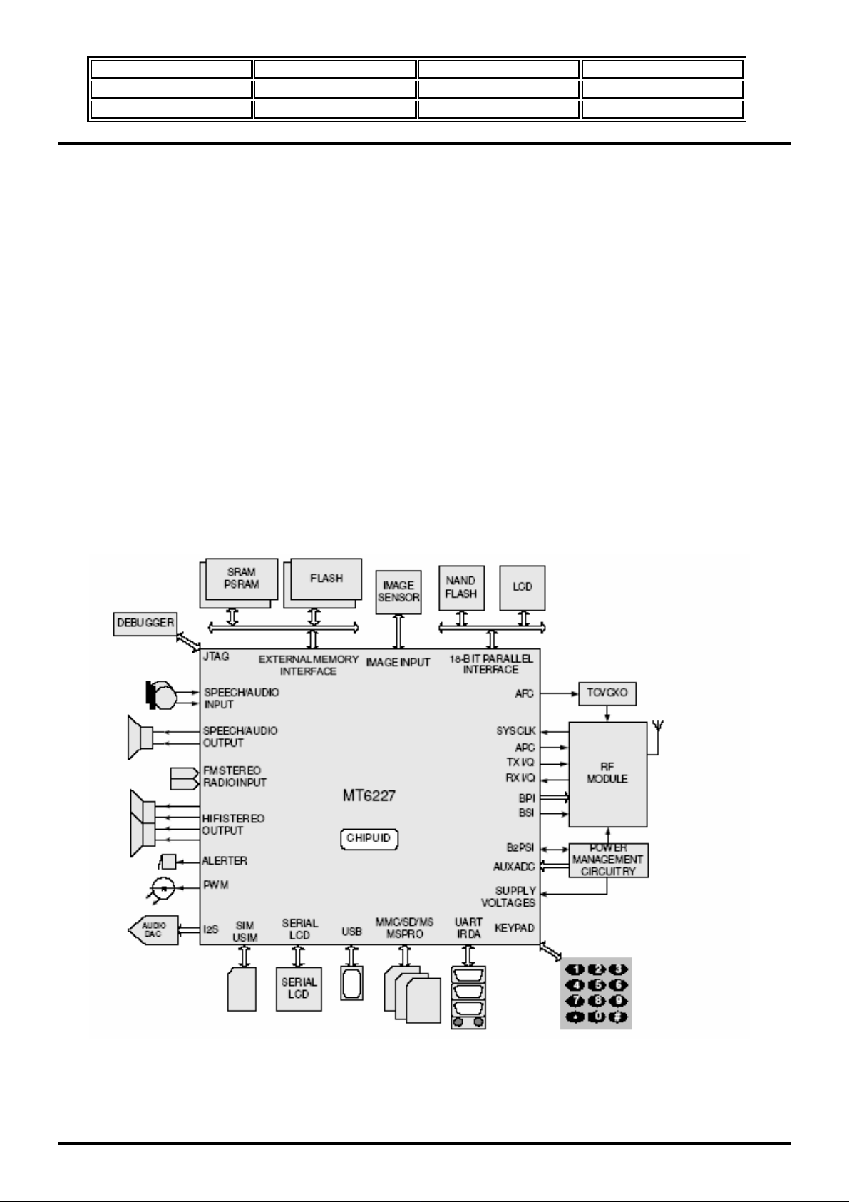
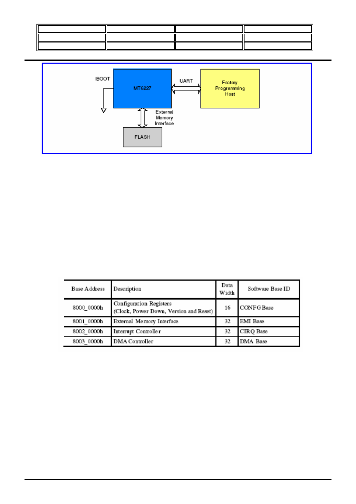
The Figure 1 is shown Typical Application for MT6227.
Figure 1 : Typical Application for MT6227
DS1 TECHNICAL MANUAL Page 3.1
Page 2

MODEL DS1 VERSION V 0.2
PREPARED BY H/W DATE 04/07/2008
SUBJECT TECHNICAL MANUAL PAGE 2/113
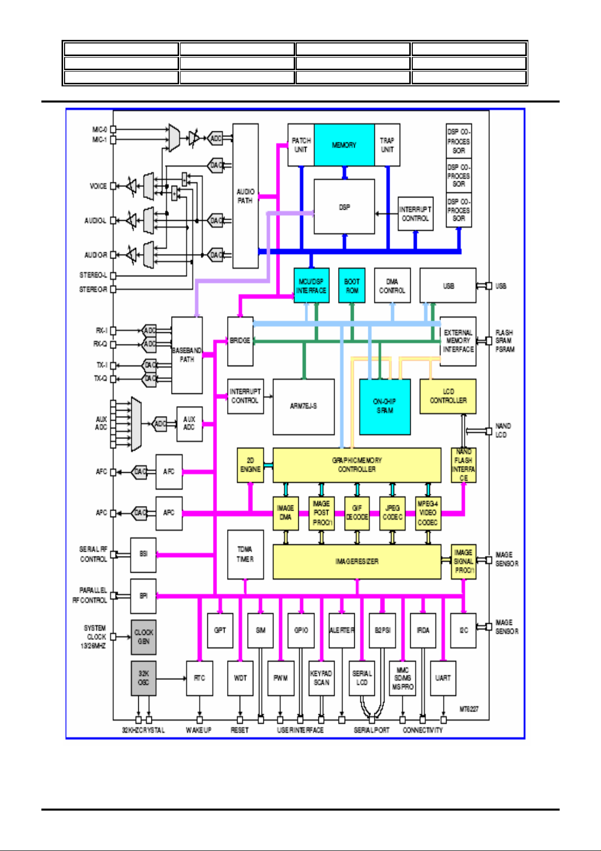
Figure 2 is shown the Block Diagram of MT6227 in detail.
DS1 TECHNICAL MANUAL Page 3.2
Page 3
MODEL DS1 VERSION V 0.2
PREPARED BY H/W DATE 04/07/2008
SUBJECT TECHNICAL MANUAL PAGE 3/113
Figure 2 : Block Diagram of MT6227
DS1 TECHNICAL MANUAL Page 3.3
Page 4
MODEL DS1 VERSION V 0.2
PREPARED BY H/W DATE 04/07/2008
SUBJECT TECHNICAL MANUAL PAGE 4/113
2. Product Description
2.1 Pin Outs
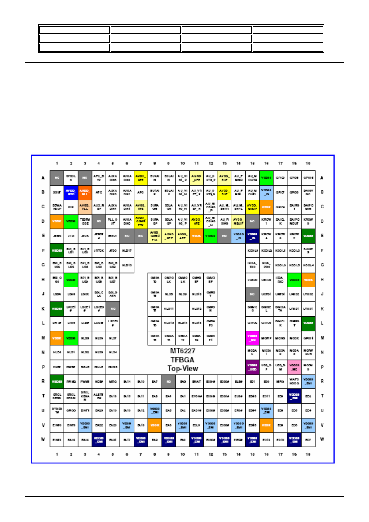
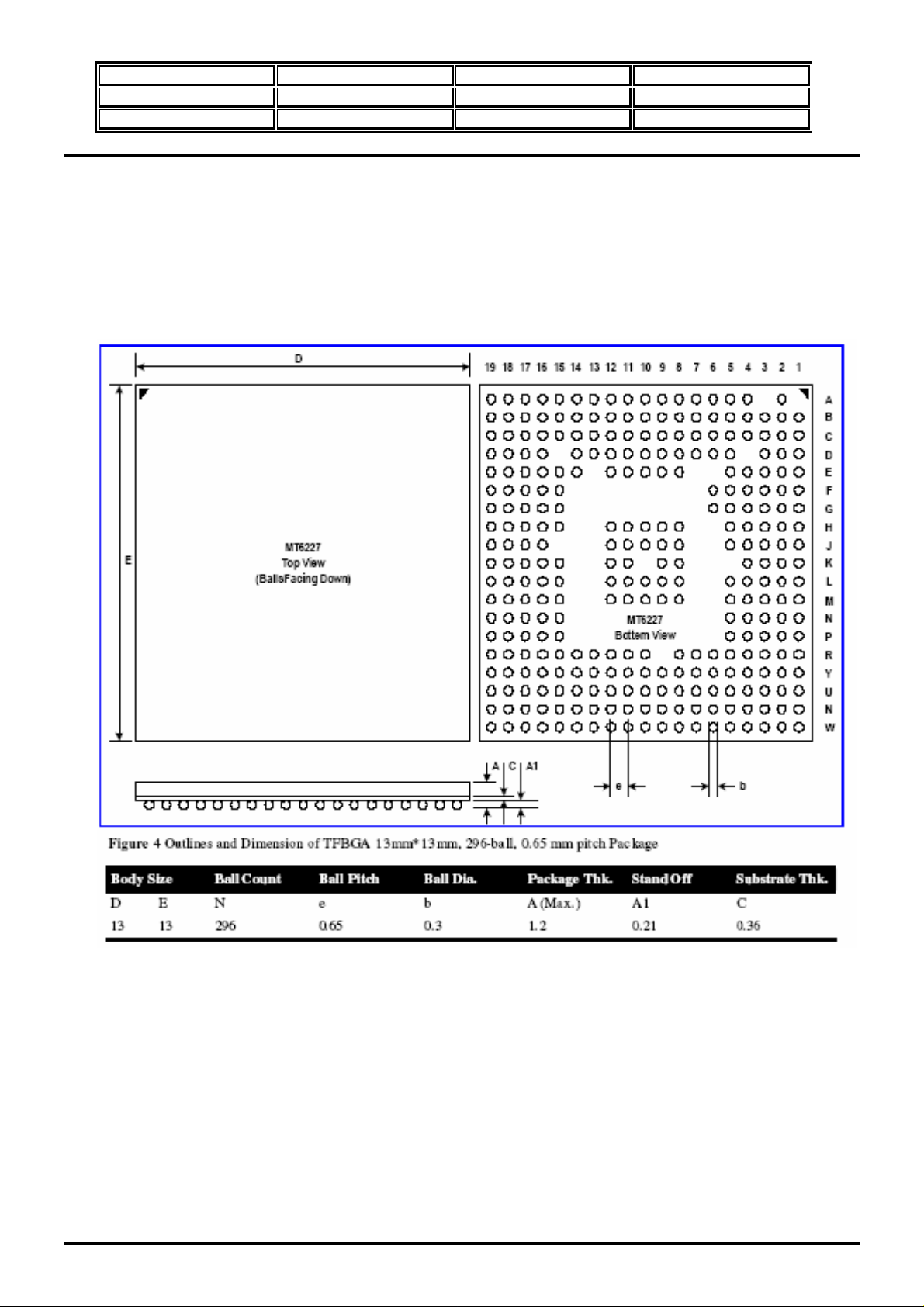
One type of Package for this product, TFBGA 13x13mm, 296balls, 0.65mm pitch package, is offered.
Pin outs and the top view are illustrated in Figure 3,4.
-. Pin Out
Figure 3 . MT6227 Pin Out.
DS1 TECHNICAL MANUAL Page 3.4
Page 5
MODEL DS1 VERSION V 0.2
PREPARED BY H/W DATE 04/07/2008
SUBJECT TECHNICAL MANUAL PAGE 5/113
-. Top and Bottom View
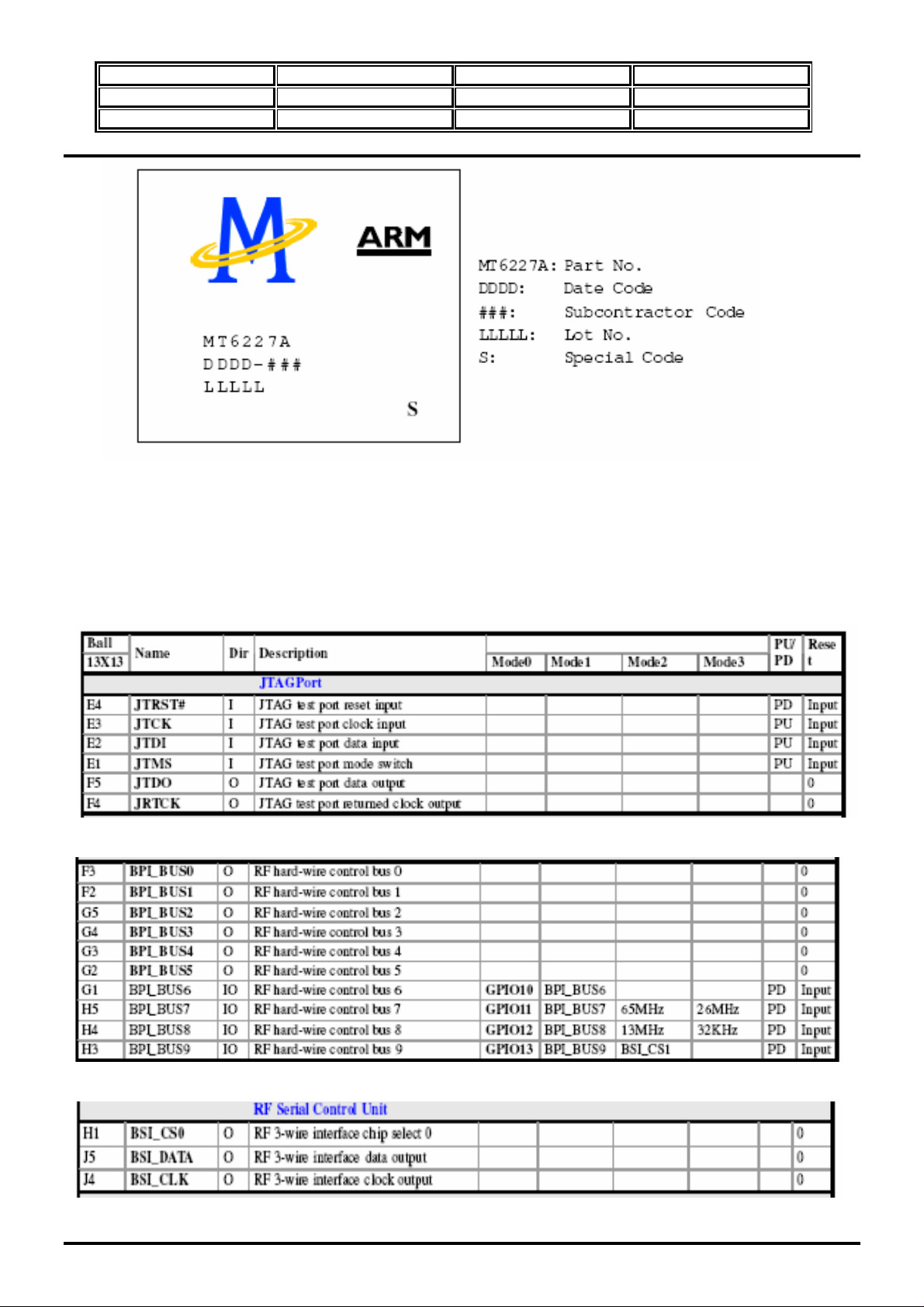
2.2 Top Masking Definition
DS1 TECHNICAL MANUAL Page 3.5
Page 6
MODEL DS1 VERSION V 0.2
PREPARED BY H/W DATE 04/07/2008
SUBJECT TECHNICAL MANUAL PAGE 6/113
Figure 5. Top masking definition
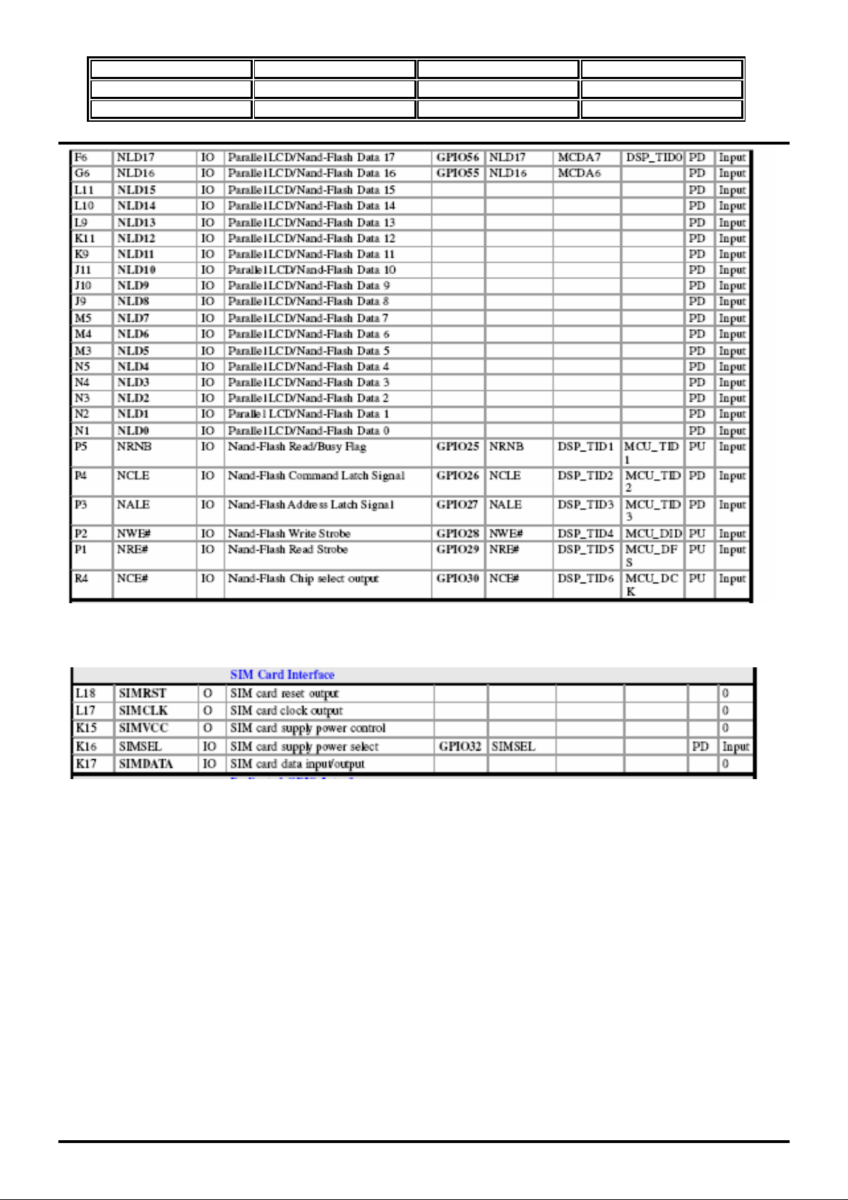
2.3 Pin Description
-. JTAG Port
-. RF Parallel Control Unit
-. RF Serial Control Unit
DS1 TECHNICAL MANUAL Page 3.6
Page 7

MODEL DS1 VERSION V 0.2
PREPARED BY H/W DATE 04/07/2008
SUBJECT TECHNICAL MANUAL PAGE 7/113
-. PWM Interface
-. Serial LCD/PM IC Interface
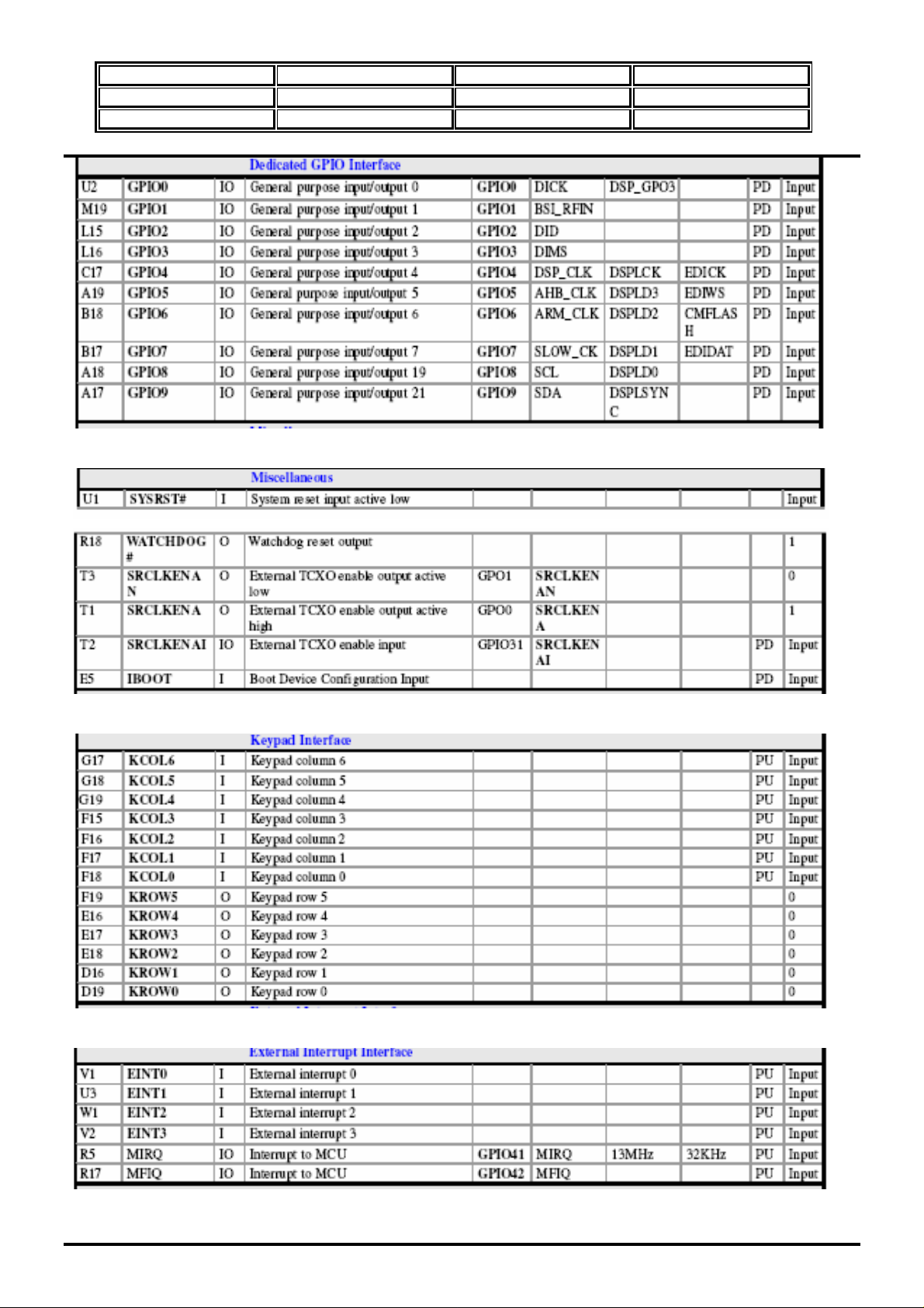
-. Parallel LCD/Nand_Flash Interface
DS1 TECHNICAL MANUAL Page 3.7
Page 8
MODEL DS1 VERSION V 0.2
PREPARED BY H/W DATE 04/07/2008
SUBJECT TECHNICAL MANUAL PAGE 8/113
-. SIM Card Interface
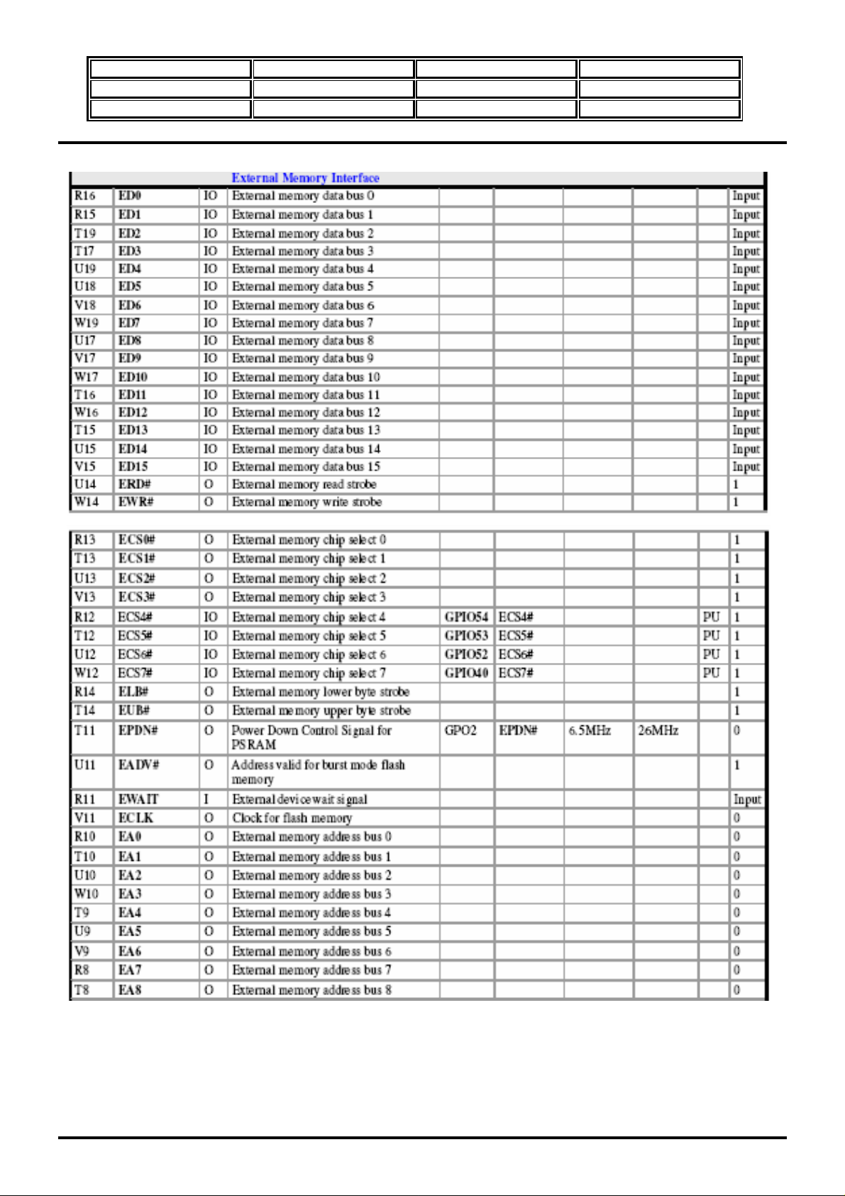
-. Dedicated GPIO Interface
DS1 TECHNICAL MANUAL Page 3.8
Page 9
MODEL DS1 VERSION V 0.2
PREPARED BY H/W DATE 04/07/2008
SUBJECT TECHNICAL MANUAL PAGE 9/113
-. Miscellaneous
-. Key Pad Interface
-. External Interrupt Interface
DS1 TECHNICAL MANUAL Page 3.9
Page 10
MODEL DS1 VERSION V 0.2
PREPARED BY H/W DATE 04/07/2008
SUBJECT TECHNICAL MANUAL PAGE 10/113
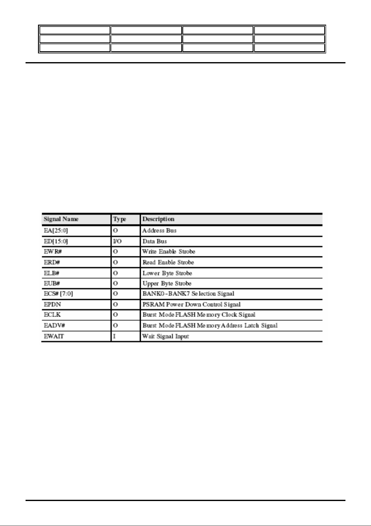
-. External Memory Interface
DS1 TECHNICAL MANUAL Page 3.10
Page 11
MODEL DS1 VERSION V 0.2
PREPARED BY H/W DATE 04/07/2008
SUBJECT TECHNICAL MANUAL PAGE 11/113
-. USB Interface
-. Memory Card Interface
-. UART Interface
DS1 TECHNICAL MANUAL Page 3.11
Page 12
MODEL DS1 VERSION V 0.2
PREPARED BY H/W DATE 04/07/2008
SUBJECT TECHNICAL MANUAL PAGE 12/113
-. Digital Audio Interface
-. Image Sensor Interface
-. Analog Interface
DS1 TECHNICAL MANUAL Page 3.12
Page 13
MODEL DS1 VERSION V 0.2
PREPARED BY H/W DATE 04/07/2008
SUBJECT TECHNICAL MANUAL PAGE 13/113
-. VCXO Interface
-. RTC Interface
DS1 TECHNICAL MANUAL Page 3.13
Page 14
MODEL DS1 VERSION V 0.2
PREPARED BY H/W DATE 04/07/2008
SUBJECT TECHNICAL MANUAL PAGE 14/113
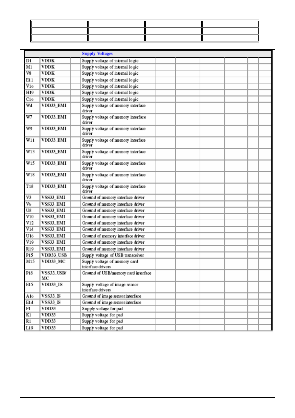
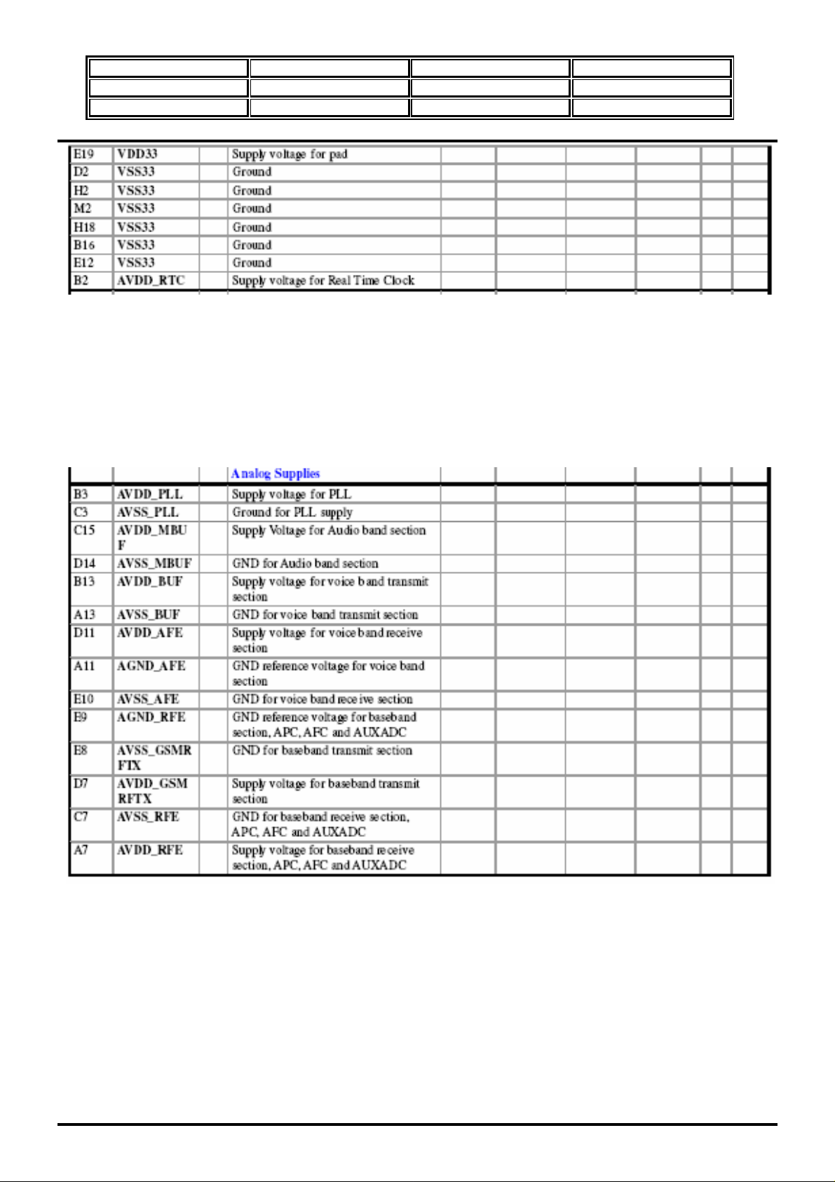
-. Supply Voltages
DS1 TECHNICAL MANUAL Page 3.14
Page 15
MODEL DS1 VERSION V 0.2
PREPARED BY H/W DATE 04/07/2008
SUBJECT TECHNICAL MANUAL PAGE 15/113
DS1 TECHNICAL MANUAL Page 3.15
Page 16
MODEL DS1 VERSION V 0.2
PREPARED BY H/W DATE 04/07/2008
SUBJECT TECHNICAL MANUAL PAGE 16/113
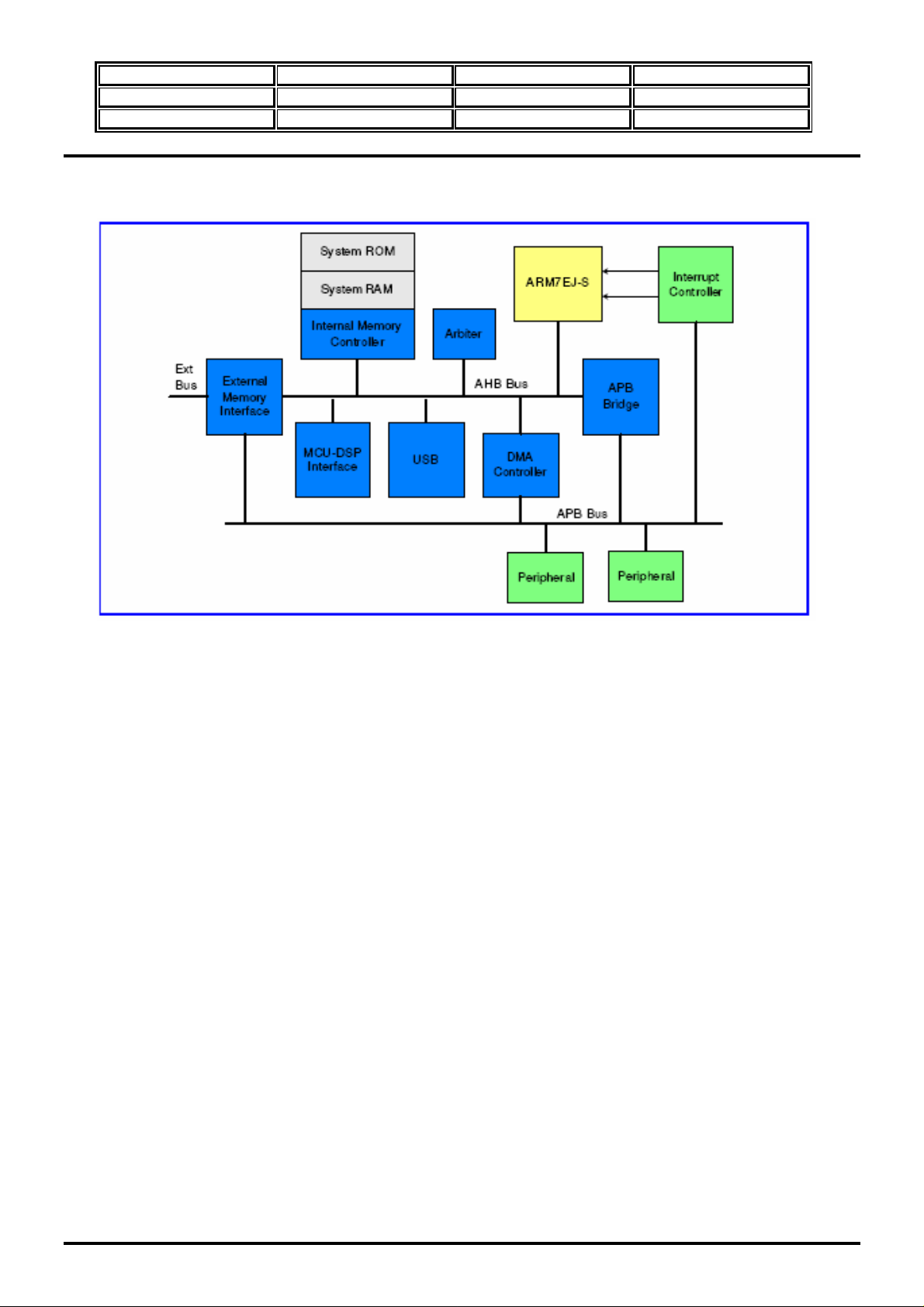
3. Micro-Controller Unit Subsystem
Figure 6 illustrates the block diagram of the Micro-Controller Unit Subsystem in MT6227. The
Subsystem utilizes a main 32-bit ARM7EJ-S RISC processor, which plays the role of the main bus
master controlling the whole subsystem. The processor communicates with all the other on-chip
modules via the two-level system buses: AHB Bus and APB Bus. All bus transactions originate from
bus masters, while salves can only respond to requests from bus masters. Before data transfer can be
DS1 TECHNICAL MANUAL Page 3.16
Page 17
MODEL DS1 VERSION V 0.2
PREPARED BY H/W DATE 04/07/2008
SUBJECT TECHNICAL MANUAL PAGE 17/113
established, bus master must ask for bus ownership. This is accomplished by request-grant
handshaking protocol between masters and arbiters.
Figure 6. Block Diagram of MCU in MT6227
3.1 Processor Core
The Micro-Controller Unit subsystem in MT6227 uses the 32-bit Arm7EJ-S RISC processor that is
based on the Von Neumann architecture with a single 32-bit data bus carrying both instructions and
data. The memory interface of ARM7EJ-S is totally compliant to AMBA based bus system, which allows
direct connection to the AHB Bus.
3.2 Memory Management
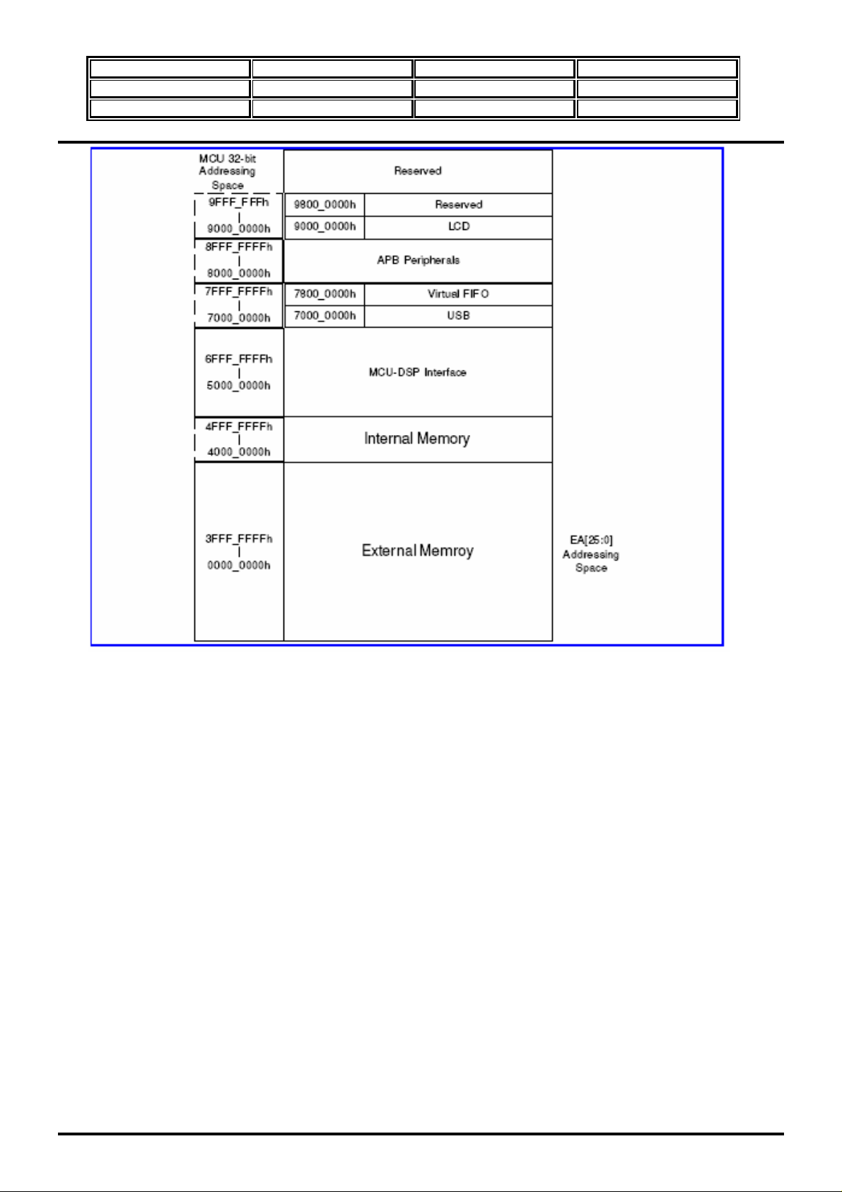
The processor core of MT6227 supports only memory addressing method for instruction fetch and data
access. It manages a 32bit address space that has addressing capability up to 4GB. System RAM,
System ROM , Registers, MCU Peripherals and external components are all mapped onto such 32-bit
address space, as depicted in Figure 7.
DS1 TECHNICAL MANUAL Page 3.17
Page 18
MODEL DS1 VERSION V 0.2
PREPARED BY H/W DATE 04/07/2008
SUBJECT TECHNICAL MANUAL PAGE 18/113
Figure 7. Memory Layout of MT6227
External Memory Access
To allow external access, The MT6227 outputs 26bits(A25~A0) of address line along with 8 selection
signals that correspond to associated memory blocks. This is, MT6227 can support up to 8 MCU
addressable external components. The data width of internal system bus is fixed at 32bit wide, while
the data width of the external components can be either 8 or 16 bits.
Factory Programming
The configuration for factory programming is shown in Figure 8. Usually the factory programming host
connects with MT6227 via the UART interface. In order to have it work properly, the system should
boot up from Boot Code. That is, IBOOT should be tied to GND. The download speed can be up to
921K bps while MCU is running at 26Mhz. After the system has reset, the Boot Code will guide the
processor to run the Factory Programming software placed in System ROM. Then, MT6227 will start
and continue to poll the UART1 port until valid information is detected. The first information received
on the UART1 will be used to configure the chip for factory programming. The Flash downloader
program is then transferred in to System RAM or external SRAM.
DS1 TECHNICAL MANUAL Page 3.18
Page 19
MODEL DS1 VERSION V 0.2
PREPARED BY H/W DATE 04/07/2008
SUBJECT TECHNICAL MANUAL PAGE 19/113
Figure 8. Factory Programming
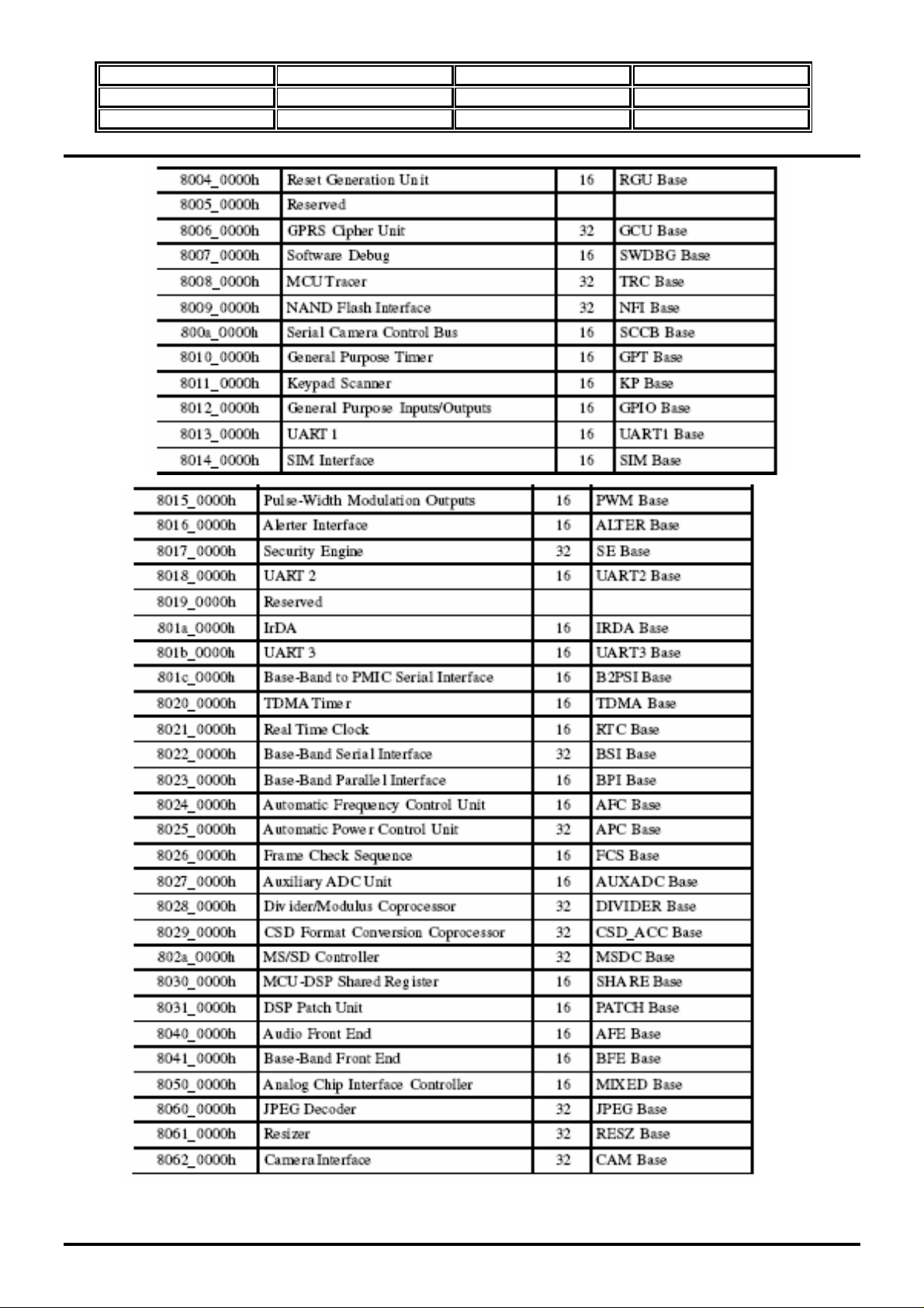
3.3 Bus System
Two levels of bus hierarchy are employed in the Micro-Controller Unit Subsystem of MT6227. As depicted
in Figure5, AHB Bus and APB Bus serve as system backbone and peripheral buses, while an APB bridge
connects these two buses. Both AHB and APB Buses operate at the same clock rate as processor core.
The APB Bridge is the only bus master residing on the APB Bus. All APB slaves are mapped onto memory
block MB8 in MCU 32bit addressing space. A central address decoder is implemented inside the bridge to
generate select signals for individual peripherals. In addition, since the base address of each APB slave has
been associated with select signals, the address bus on APB will contain only the value of offset address.
The base address and data width of each peripheral are listed in below table.
DS1 TECHNICAL MANUAL Page 3.19
Page 20
MODEL DS1 VERSION V 0.2
PREPARED BY H/W DATE 04/07/2008
SUBJECT TECHNICAL MANUAL PAGE 20/113
DS1 TECHNICAL MANUAL Page 3.20
Page 21
MODEL DS1 VERSION V 0.2
PREPARED BY H/W DATE 04/07/2008
SUBJECT TECHNICAL MANUAL PAGE 21/113
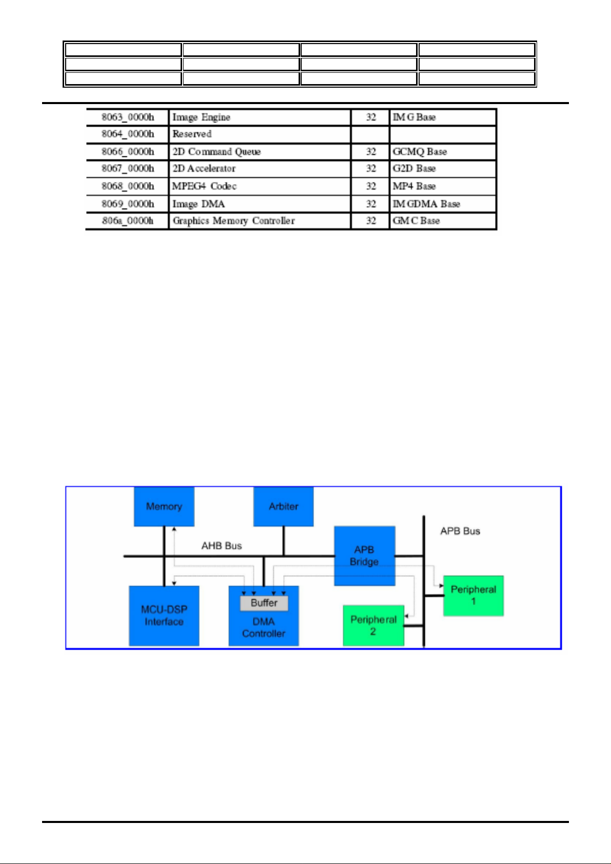
3.4 Direct Memory Access
A generic DMA controller is placed on Layer2 AHB Bus to support fast data transfer snd to off-load the
processor. With this controller, specific devices on AHB or APB buses can benefit greatly from quick
completion of data movement from or to memory modules such as Internal System Ram or External
SRam. Such generic DMA Controller can also be used to connect any two devices other than memory
module as long as they can be addressed in memory space.
Figure 9. Variety data paths of DMA transfer.
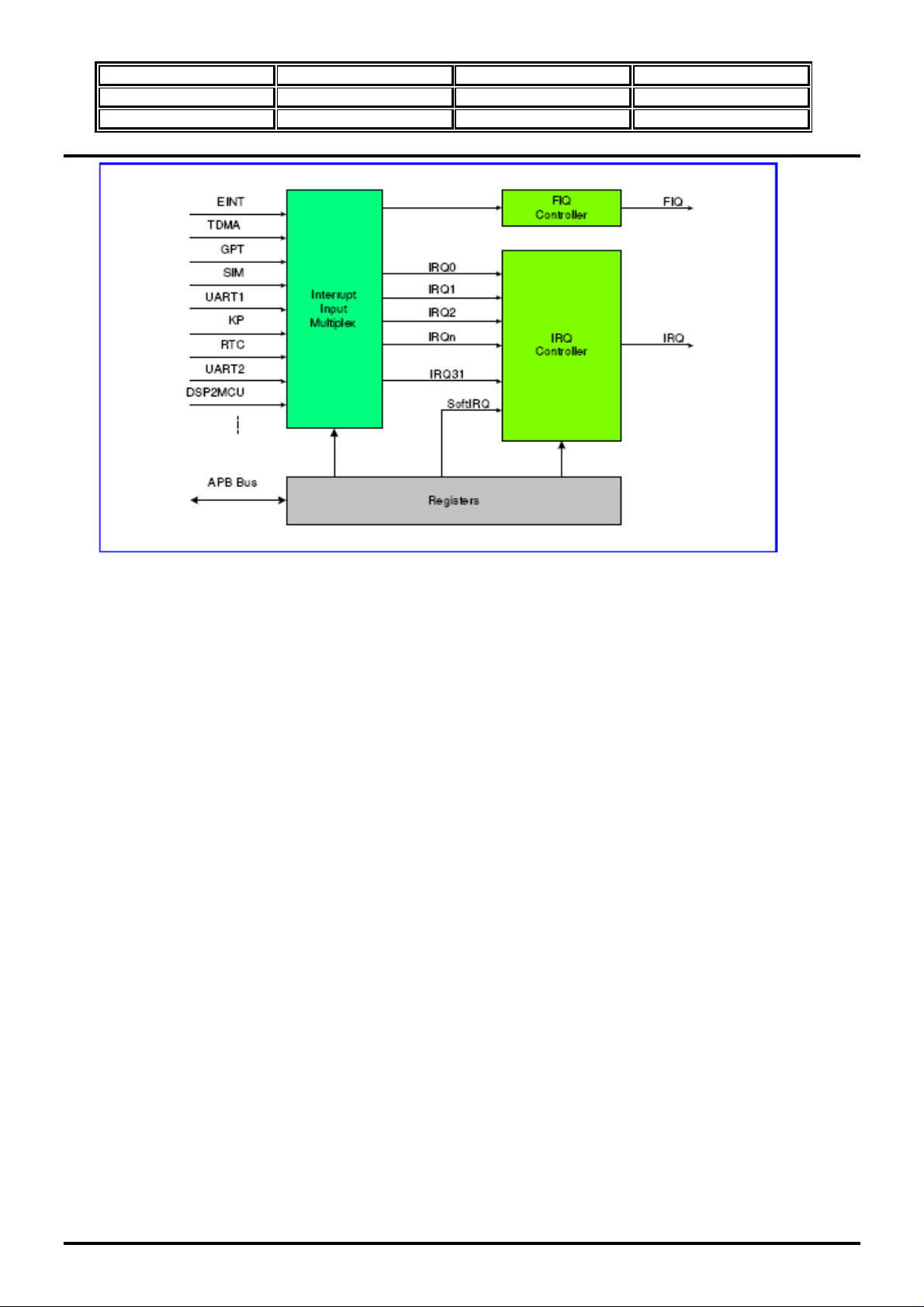
3.5 Interrupt Controller
Figure 10 outlines the major functionality of the MCU Interrupt Controller. The interrupt controller
processes all interrupt sources coming from external lines and internal MCU peripherals. Since
ARM7EJ-S core supports two levels of interrupt latency. This controller generates two request signals :
FIQ for fast, low latency interrupt request and IRQ for more general interrupts with lower priority.
DS1 TECHNICAL MANUAL Page 3.21
Page 22
MODEL DS1 VERSION V 0.2
PREPARED BY H/W DATE 04/07/2008
SUBJECT TECHNICAL MANUAL PAGE 22/113
Figure 10. Block Diagram of Interrupt controller.
External Interrupt
This interrupt controller also integrates an External Interrupt controller that can support up to 4 interrupt
requests coming from external sources, the EINT0~3 and 4 wake up interrupt requests. The four
external interrupts can be used for different kind of applications, mainly for event detections : detection
of hand free connection, detection of hood opening, detection of battery charger connection.
In DS1, external interrupts are used for Headset detection, Charger Detection and Blue Tooth Detection.
3.6 Internal Memory Interface
System Ram
MT6227 provides one 284Kbyte size of on-chip memory modules acting as System Ram for data access
with low latency. Such a Module is composed of three high speed synchronous SRAMs with AHB Slave
interface connected to the system backbone AHB Bus. Bank 0 and bank 1 SRAMs are 128Kbyte and Bank 2
SRAM is 28Kbyte. The synchronous SRAM operates on the same clock as the AHB Bus and is organized as
32bits wide with 4 byte-write signals capable for byte operations. Band 0 and Band 1 SRAM macros have
limited repair capability. The yield of SRAM is improved if the defects inside it can be repaired urging testing.
System ROM
The 27Kbyte System ROM is primarily used to store software program for Factory programming.. However,
due to its advantageous low latency performance, some of the timing critical codes are also placed in
DS1 TECHNICAL MANUAL Page 3.22
Page 23
MODEL DS1 VERSION V 0.2
PREPARED BY H/W DATE 04/07/2008
SUBJECT TECHNICAL MANUAL PAGE 23/113
System ROM. This module is composed of high-speed VIA ROM with an AHB Slave Interface connected to
a system backbone.
3.7 External Memory Interface
MT6227 incorporates a powerful and flexible memory controller, External Memory Interface, to connect with
a variety of memory components. This controller provides one generic access scheme for FLASH memory,
SRAM and PSRAM. Up to 8 memory banks can be supported simultaneously, ban 0 ~ Bank 7, with a
maximum size of 64MB each.
Since more of the Flash Memory, SRAM and PSRAM have similar ac requirements, a generic configuration
scheme to interface them is desired. This way, the software program can treat different components by
simply specifying certain predefined parameters. All these parameters are based on cycle time of system
clock.
External Memory Interface of MT6227 for Asynchronous/Synchronous components.
In DS1, ECS0# is used for External Flash Memory and ECS1# is used for External PSRAM.
4. Microcontroller Peripherals
Microcontroller(MCU) Peripherals are devices that are under direct control of the Microcontroller. Most of
the devices are attached to the Advanced Peripheral Bus(APB) of the MCU subsystem, and serve as APB
slaves. Each MCU peripheral must be accessed as a memory-mapped I/O device: that is, the MCU or the
DMA bus master reads from or writes to the specific peripheral by issuing memory-addressed transactions.
4.1 Pulse-Width Modulation Outputs.
Two generic Pulse-Width Modulators are implemented to generate pulse sequences with programmable
frequency and duty cycle for LCD backlight or charging purpose. The duration of the PWM output signal is
low as long as the internal counter value is greater than or equal to the threshold value.
In DS1, PWM1 is used for LCD Module Backlight Enable and PWM2 is used for Flash LED Enable.
DS1 TECHNICAL MANUAL Page 3.23
Page 24
MODEL DS1 VERSION V 0.2
PREPARED BY H/W DATE 04/07/2008
SUBJECT TECHNICAL MANUAL PAGE 24/113
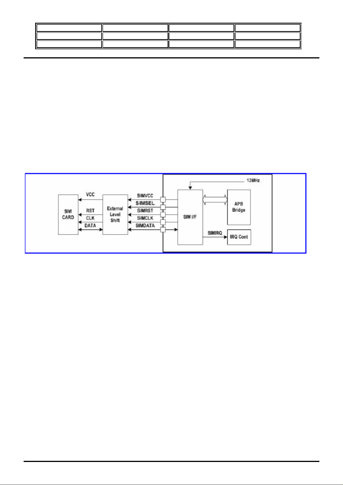
4.2 SIM Interface
The MT6227 contains a dedicated smart card interface to allow the MCU access to the SIM Card. It can
operate via 5 terminals, using SIMVCC, SIMSEL, SIM RST, SIMCLK and SIMDATA.
The SIMVCC is used to control the external voltage supply to the SIM card and SIMSEL determines the
regulated smart card supply voltage. SIMRST is used as the SIM card reset signal. Besides, SIMDATA and
SIMCLK are used for data exchange purpose. Basically, the SIM interface acts as a half duplex
asynchronous communication port and its data format is composed of ten consecutive bits: a start bit in
state Low, eight information bits and a tenth bit used for parity checking.
In DS1, Only 3V SIM interface is used.
Figure 11. SIM interface
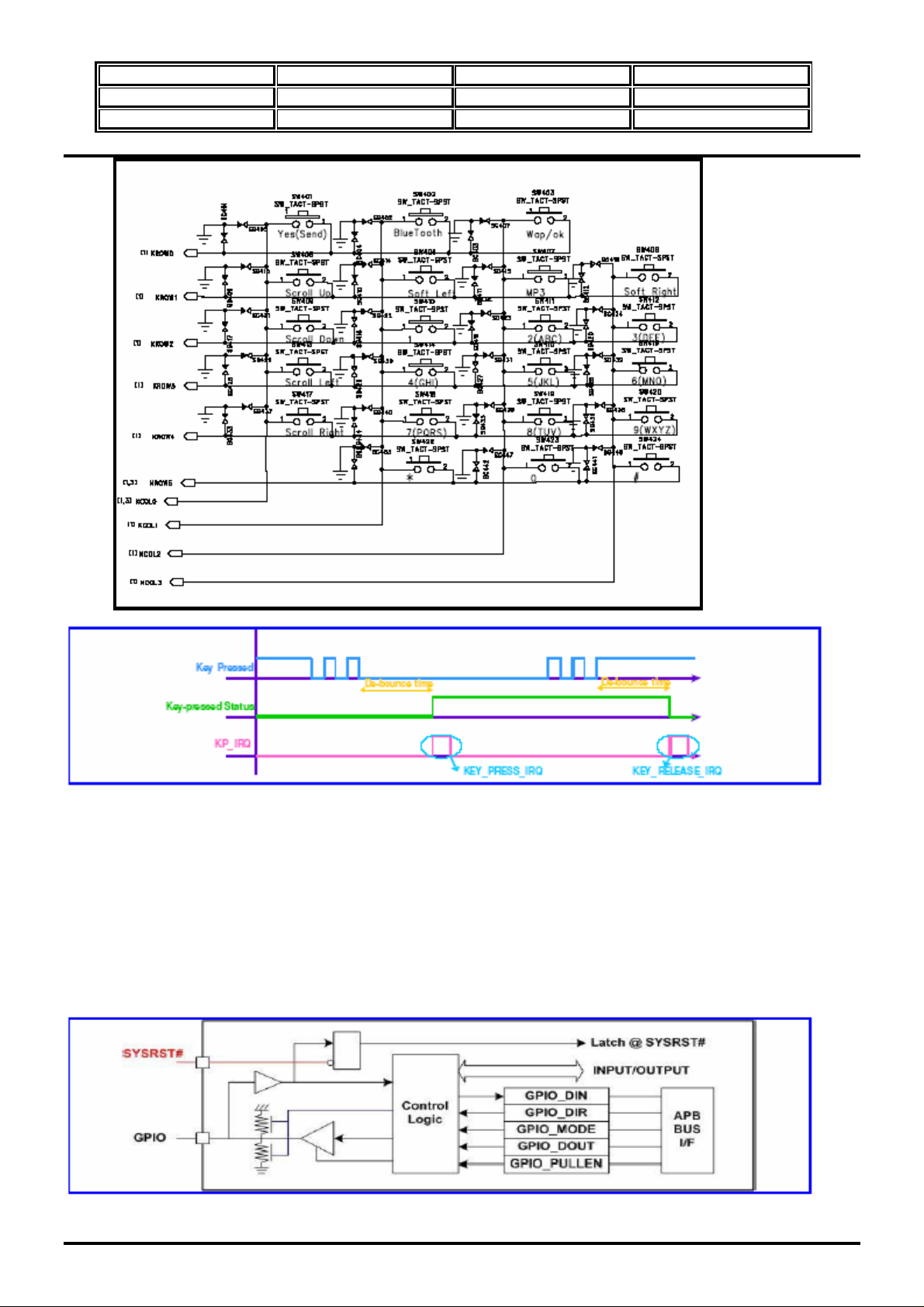
4.3 Keypad Scanner
The keypad can be divided into two parts : One is the keypad interface including 7 columns and 6 rows
The other is the key detection block which provides key pressed, key released and de-bounce mechanism.
Each time the key is pressed or released, i.e. something different in the 7x6 matrix, the key detection block
will sense it, and it will start to recognize if it is a key pressed or key released event. Whenever the key
status changes and is stable, a KEYPAD IRQ will be issued. The MCU can then read the key pressed
directly in KP_HI_KEY, KP_MID_KEY and KP_LOW_KEY register.
In DS1, The 6 Rows are used (Row0 ~Row5) and The 6 Columns are used (Col 0~4 and Col 6)
DS1 TECHNICAL MANUAL Page 3.24
Page 25
MODEL DS1 VERSION V 0.2
PREPARED BY H/W DATE 04/07/2008
SUBJECT TECHNICAL MANUAL PAGE 25/113
Figure 12. Key pressed with de-bounce mechanism
4.4 General Purpose Inputs/Outputs
MT6227 offers 57 general purpose I/O pins and 5 general-purpose output pins. By setting the control
registers, MCU software can control the direction, the output value and read the input values on these pins.
These GPIOs and GPOs are multiplexed with other functionalities to recude the pin count.
Upon hardware reset(/SYSRST), GPIOs are all configured as inputs.
DS1 TECHNICAL MANUAL Page 3.25
Page 26
MODEL DS1 VERSION V 0.2
PREPARED BY H/W DATE 04/07/2008
SUBJECT TECHNICAL MANUAL PAGE 26/113
Figure 13. GPIO Block diagram.
4.5 General Purpose Timer
Three general-purpose timers are provided. The Timers are 16 bits long and run independently of each
other, although they share the same clock source. Two timers can operate in one of two modes: one-shot
mode and auto-repeat mode; the other is a free running timer. In one-shot mode, When the timer counts
down and reaches zero, it is halted. In auto-repeat mode, when the timer reaches zero, it simply resets to
countdown initial value and repeats the countdown to zero; this loop repeats until the disable signal is set to
1.
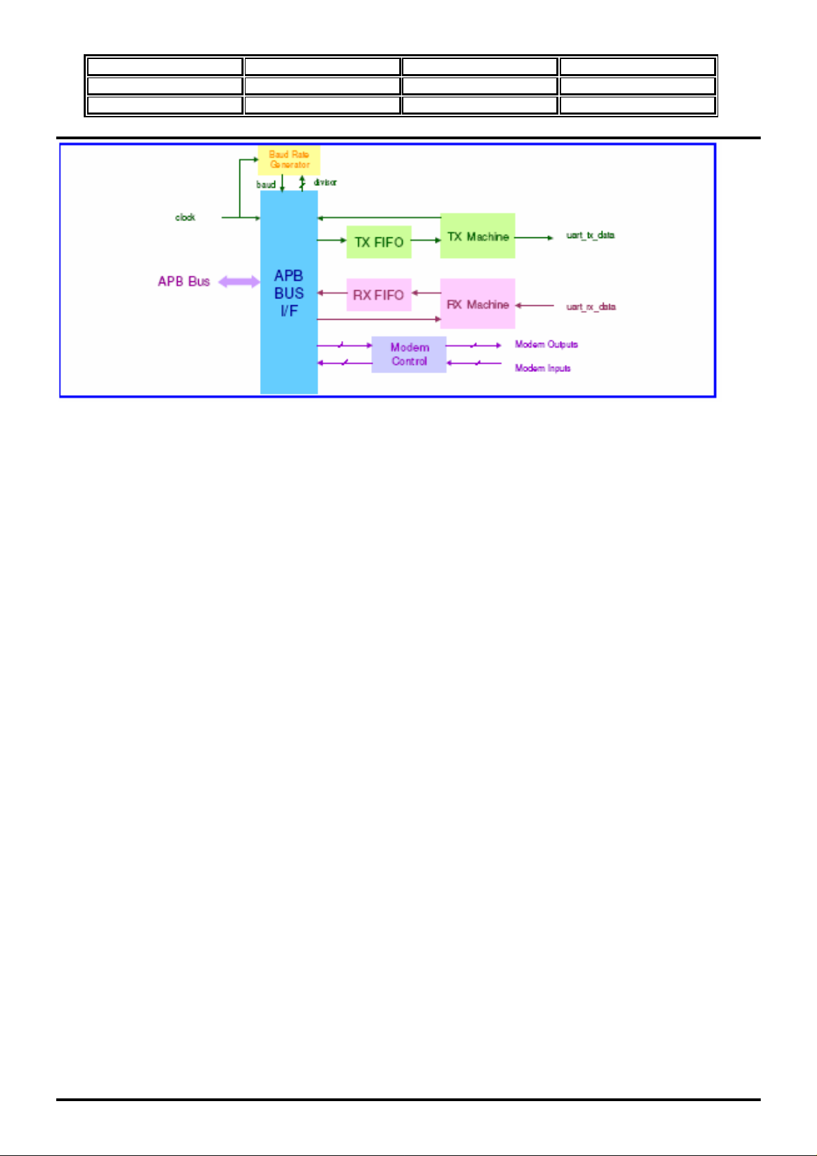
4.6 UART
The baseband chipset houses three UARTs. The UARTs provide full duplex serial communication channels
between baseband chipset and external devices.
In DS1, UART1(URXD1, UTXD1) is used for Factory Programming and UART3(URXD3, UTXD3) is used for
Blue Tooth Programming.
DS1 TECHNICAL MANUAL Page 3.26
Page 27
MODEL DS1 VERSION V 0.2
PREPARED BY H/W DATE 04/07/2008
SUBJECT TECHNICAL MANUAL PAGE 27/113
Figure 14. UART block diagram.
RX data Timeout Interrupt :
When virtual FIFO mode is disabled, RX data Timeout Interrupt is generated if all of the following apply :
1. FIFO contains at least on character.
2. The most recent character was received longer than four character periods ago(including all start,
parity and stop bit)
3. The most recent CPU read of the FIFO was longer than four character periods ago.
When virtual FIFO mode is enabled, RX Data timeout Interrupt is generated if all of the following apply:
1. FIFO is empty.
2. The most recent character was received longer than four character periods ago(including all start,
parity and stop bit)
3. The most recent CPU read of the FIFO was longer than four character periods ago
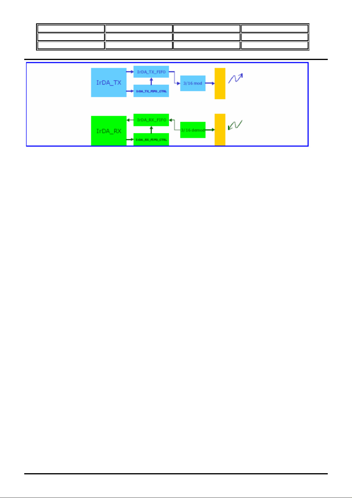
4.7 IrDA framer
IrDA framer, which is depicted in Figure 15, is implemented to reduce the CPU loading for IrDA
transmission. IrDA framer functional block can be divided into two parts : the transmitting part and the
receiving part. In the transmitter, it will perform BOFs addition, byte stuffing, the addition of 16bits FCS and
EOF appendence. In the receiving part, it will execute BOFs removal, ESC character removal, CRC checking
and EOF detection. In addition, the framer will perform 3/16 modulation and demodulation to connect to the
IR transceiver. The transmitter and receiver all need DMA channel.
DS1 TECHNICAL MANUAL Page 3.27
Page 28
MODEL DS1 VERSION V 0.2
PREPARED BY H/W DATE 04/07/2008
SUBJECT TECHNICAL MANUAL PAGE 28/113
Figure 15. IrDA Block Diagram.
4.8 Read Time Clock
The Real Time Clock(RTC) module provides time and data information. The clock is based on a 32.768Khz
oscillator with an independent power supply. When the mobile handset is powered off, a dedicated
regulator supplies the RTC block. If the main battery is not present, a backup supply such as a small
mercury cell battery or a large capacitor is used. In addition to providing timing data, an alarm interrupt is
generated and can be used to power up the baseband core via the BBWAKEUP pin. Regulator interrupts
corresponding to seconds, minutes, hours and days can be generated whenever the time counter value
reaches a maximum value. The Maximum day-of-month values, which depend on the leap year condition,
are stored in the RTC block.
In DS1, Big Capacitor Battery(BAT100) is used for Backup Battery. The Charging Voltage is about 1.5V by
VRTC.
4.9 Auxiliary ADC Unit
The auxiliary ADC unit is used to monitor the status of battery and charger, identify the plugged peripheral
and perform temperature measurement. There provides 7 input channels for diversified application in this
unit. There provides 2 modes of operation : immediate mode and timer-triggered mode.
5. Microcontroller Coprocessors
Microcontroller Coprocessors are designed to run computing-intensive processes in place of the
Microcontroller(MCU). These coprocessors especially target timing critical GSM/GPRS Model processes
that require fast response and large data movement. Controls to the coprocessors are all through
memory access via the APB.
6. Multi-Me dia Subsystem
DS1 TECHNICAL MANUAL Page 3.28
Page 29
MODEL DS1 VERSION V 0.2
PREPARED BY H/W DATE 04/07/2008
SUBJECT TECHNICAL MANUAL PAGE 29/113
MT6227 is specially designed to support multi-media terminals. It integrates several hardware based
accelerators such as advanced LCD display controller, hardware JPEG encoder/decoder, hardware
Image Resizer, and MPEG4 video Codec.
In addition, MT6227 also incorporates nand Flash, USB 1.1 Device and SD/MMC/MS/MS Pro Controllers
for mass data transfers and storages. This chapter describes those functional bocks in more details.
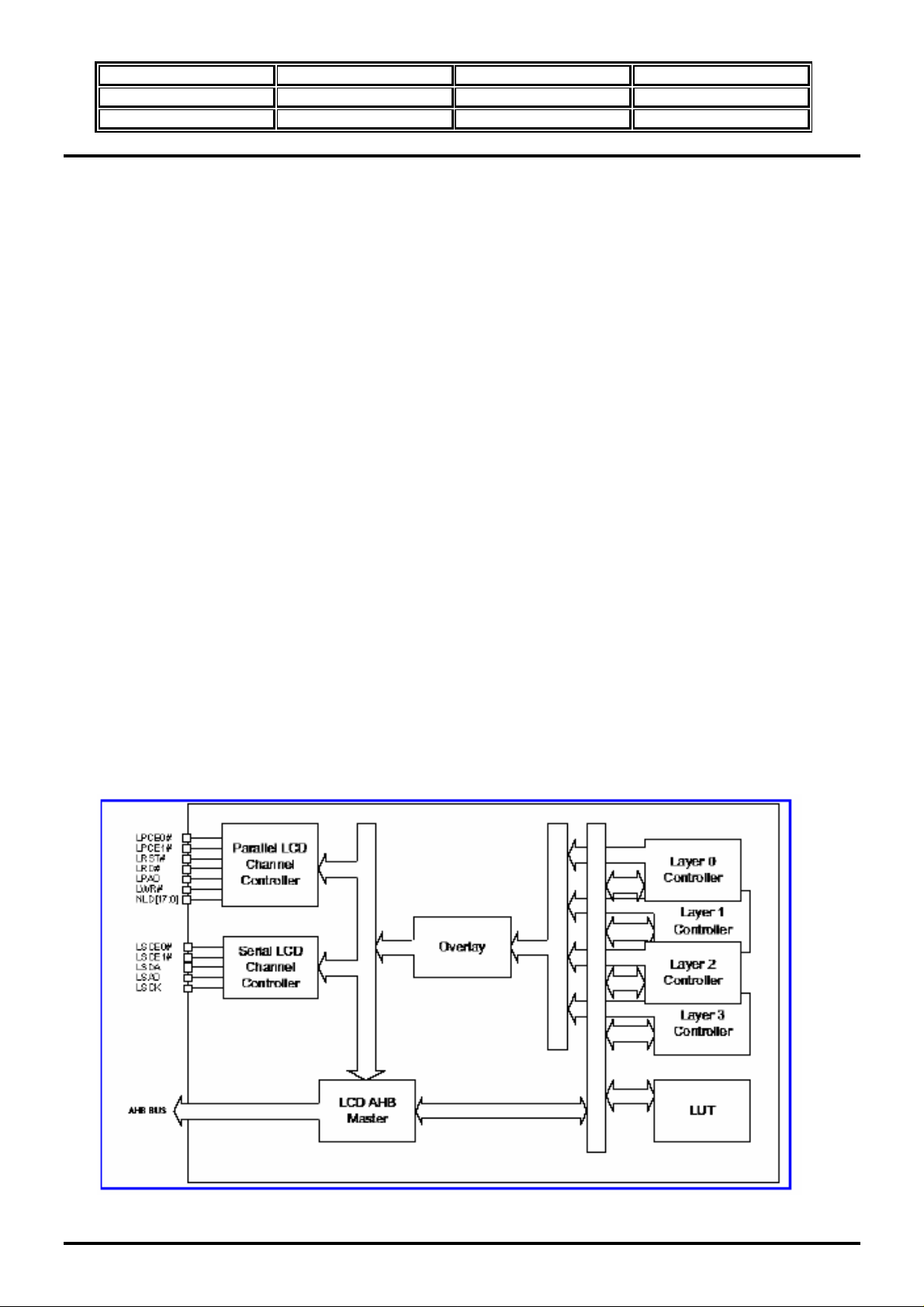
6.1 LCD Interface
MT6227 contains a versatile LCD controller which is optimized for multimedia applications. This
controller supports many types of LCD modules and contains a rich feature set to enhance the functionality.
These features are :
- Up to 320x240 resolution
- The internal frame buffer supports 8bpp indexed color and RGB 565 format
- Supports 8bpp(RGB332), 12bpp(RGB444), 16bpp(RGB5650, 18bit(RGB666) and 24bit(RGB888) LCD
modules
- 4 Layers overlay with individual color depth, window size, vert ical and horizontal offset, source key,
alpha value and
o
Display rotation control(90
,180o,270o, mirror and mirror then 90o, 180o and 270o)
- One Color Loop-up Tables.
For Parallel LCD modules, the LCD controller can reuse external memory interface or use dedicated
8/9/16/18 bit parallel interface to access them and 8080 type interface is supported. It can transfer the
display data from the internal SRAM or external SRAM/Flash Memory to the off-chip LCD modules.
DS1 TECHNICAL MANUAL Page 3.29
Page 30
MODEL DS1 VERSION V 0.2
PREPARED BY H/W DATE 04/07/2008
SUBJECT TECHNICAL MANUAL PAGE 30/113
Figure 16. LCD interface block diagram.
In DS1, The 262K color TFT LCD Module is used with Samsung Driver IC – LGDP4524.
The Resolution is 176x220 dots and 2.0inch Panel from LG Philips.
6.2 JPEG Decoder
To boost JPGE image processing performance, a hardware block is preferred to aid software and deal
with jpeg file as much as possible. As a result, JPEG Decoder is designed to decode all baseline and
progressive JPEG images with all YUV sampling frequencies combinations. To gain the best speed
performance, JPEG decoder will handle all portions of JPEG files except the 17 byte SOF marker. The
software program only needs to program related control registers based on the SOF maker and wait for an
interrupt coming from hardware. Taking into consideration the limited size of memories, hardware also
supports multiple runs of JPEG progressive images and breakpoints insertion in huge JPGE files.
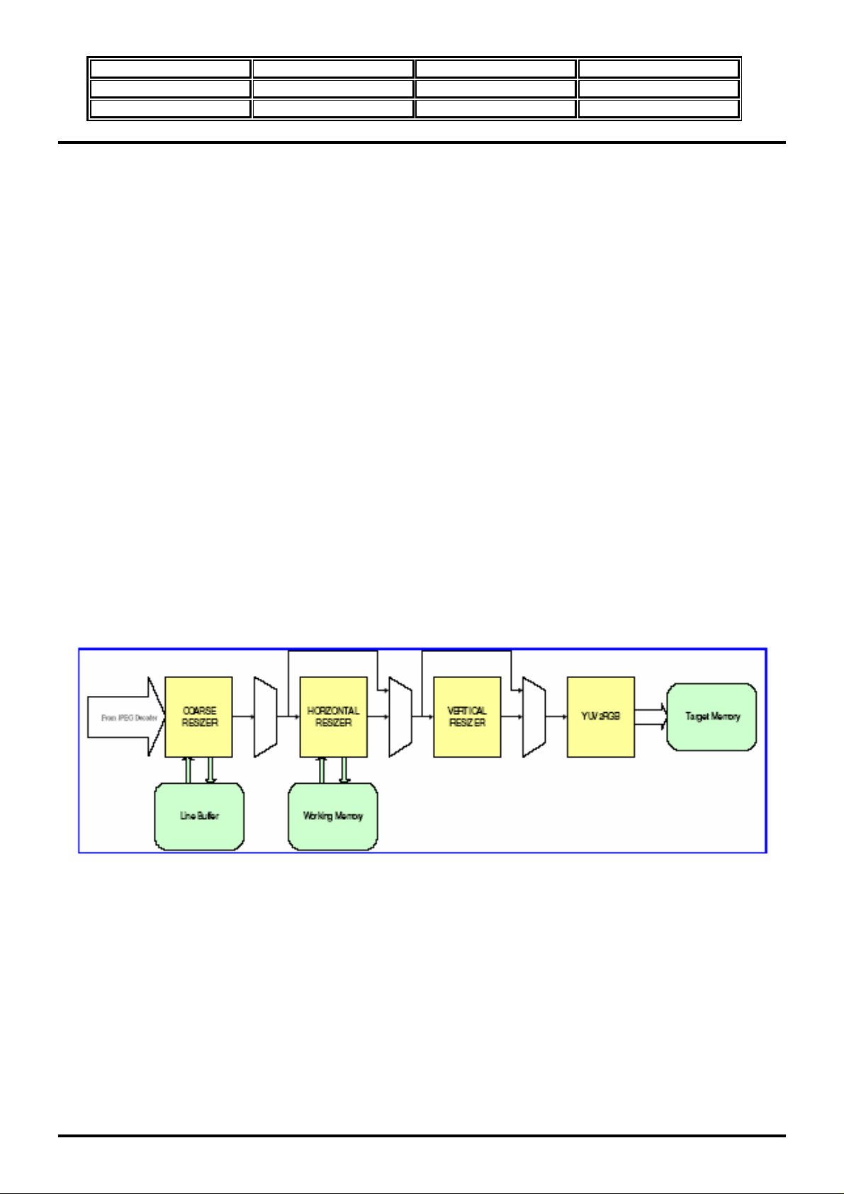
6.3 Image Resizer
This Block provides image resizing capability. It receives image data from a block-based image source
such as JPEG decoder in format of YUV color space, or a pixel-based image source such as camera in
format of RGB or YUV and performs image resizing. The first pass is coarse resizing pass and it can shrink
the image by a factor of 1, 1/4, 1/16, 1/64. The second pass is fine resizing pass and it can shrink and
enlarge the image in fractional ratio. Refer to the Figrue9 Image resizer block diagram. The maximum size of
a pixel based source image is only 2047x2047.
Figure 17. Overview of Image Resizer.
.
6.4 USB Device controller
MT6227 provides a USB function interface that is in compliance with Universal Serial Bus Specification Rev
1.1. The USB device controller supports only full-speed(12Mbps) operation. The cellular phone can make
use of this widely available USB interfaces to transmit/receive data with USB host, typically PC.
The USB device uses cable-powered feature for the transceiver but only drains little current. An external
resistor(nominally 1kohm) is required to be placed across Vusb and DP Signal. Two additional external serial
DS1 TECHNICAL MANUAL Page 3.30
Page 31

MODEL DS1 VERSION V 0.2
PREPARED BY H/W DATE 04/07/2008
SUBJECT TECHNICAL MANUAL PAGE 31/113
resistors might be needed to be placed on the output of DP and DM signals to make the output impedance
equivalent to 28~44ohm. Also, USB cable can be used to Charger for 5V input.
The ADC4_USB is to monitor whether USB cable is inserted or not.
Figure 18. USB Interface Circuit
6.5 Memory Stick and SD Memory Card Controller
The controller fully supports the SD Memory Card bus protocol as defined in SD Memory Card Specification
Part1 Physical Layer Specification version1.0. But DS1 is not interfaced Mini SD card but T-Flash Memory
Card. Interface Signals are same. Normally, the Detection is controlled by INS pin status. When Card is
nothing, The INS is high logically. And When Card inserted, The INS is low.
DS1 TECHNICAL MANUAL Page 3.31
Page 32

MODEL DS1 VERSION V 0.2
PREPARED BY H/W DATE 04/07/2008
SUBJECT TECHNICAL MANUAL PAGE 32/113
Card Detection
Figure19. Card Detection.
In DS1, The INS pin is always VSS. Because T-Flash Connector does not have a Detection Pin. So, The
Detection is done by Software programming.
6.6 Camera Interface
Figure 20. Rich Image Processor
DS1 TECHNICAL MANUAL Page 3.32
Page 33

MODEL DS1 VERSION V 0.2
PREPARED BY H/W DATE 04/07/2008
SUBJECT TECHNICAL MANUAL PAGE 33/113
MT6227 incorporates a feature rich image signal processor to connect with a variety of image sensor
components. This processor consists of timing generated unit(TG) and Lens/Sensor compensation unit
and image process unit.
So, The Camera sensor doesn’ t need the ISP block.
In DS1, Camera Sensors can be selected by BB processor. MT6227 is used, The Camera Module will be
used 2Mpixels sensor from Sharp(RJ54NBB0C).
Figure 21. Camera Sensor Interface circuit.
7. Audio Front-End
The audio front-end essentially comprises voice and audio data paths. The whole voice band data paths
are complied with GSM03.50 specification. Furthermore, Mono hands-free audio or external FM radio
playback path are provided. The stereo audio path facilitates audio quality playback, external FM radio, and
voice playback through headset.
DS1 TECHNICAL MANUAL Page 3.33
Page 34

MODEL DS1 VERSION V 0.2
PREPARED BY H/W DATE 04/07/2008
SUBJECT TECHNICAL MANUAL PAGE 34/113
Figure 22. Audio Front-End Block Diagram
Figure 23 shows the block diagram of digital circuits of the audio front-end. The APB register block is an
APB peripheral to get settings from the MCU. The DSP audio port block interfaces with the DSP for control
and data communications. Besides, there is a Digital Audio Interface(DAI) block to communicate with the
DS1 TECHNICAL MANUAL Page 3.34
Page 35

MODEL DS1 VERSION V 0.2
PREPARED BY H/W DATE 04/07/2008
SUBJECT TECHNICAL MANUAL PAGE 35/113
System Simulator for FTA or external Bluetooth module for particular applications. The digital filter block
performs filter operations for voice band and audio band signal processing.
Figure 23. The block diagram of the digital circuits for Audio Front-End
Stereo sound are implemented by TS4990 IC(Audio amplifier).
DS1 used single speaker. The AU_Out0_N/_P lines are for Voice Audio and AU_MOUTL/R are for Ring
Tone and Melody(Midi and MP3).
8. Radio Interface Control
This chapter details the MT6227 interface control with the radio part of a GSM terminal. Providing a
comprehensive control scheme, the MT6227 radio interface consists of Baseband Serial Interface(BSI),
Baseband Parallel Interface(BPI), Automatic Power Control(APC) and Automatic Frequency
Control(AFC), together with APC-DAC and AFC-DAC.
DS1 TECHNICAL MANUAL Page 3.35
Page 36

MODEL DS1 VERSION V 0.2
PREPARED BY H/W DATE 04/07/2008
SUBJECT TECHNICAL MANUAL PAGE 36/113
Figure 24. FM Radio
8.1 Baseband Serial Interface
The Baseband Serial Interface controls external radio components. A 3-wire serial bus transfers data
to RF circuitry for PLL frequency change, reception gain setting and other radio control purposes. In
this unit, BSI data registers are double-buffered in the same way as the TDMA event registers. The user
writes data into the write buffer and the data is transferred from the write buffer to the active buffer
when a TDMA_EVTVAL signal(from the TDMA timer) is pulsed.
The unit has four output pins : BSI_CLK is the output clock, BSI_DATA is the serial data port and
BSI_CS0,BSI_CS1 are the select pins for 2 external components. These outputs are connected to
MT6120 Transceiver.
DS1 TECHNICAL MANUAL Page 3.36
Page 37

MODEL DS1 VERSION V 0.2
PREPARED BY H/W DATE 04/07/2008
SUBJECT TECHNICAL MANUAL PAGE 37/113
Figure 25. BSI Unit block diagram and Timing Characteristic.
8.2 Baseband Parallel Interface
The Baseband Parallel Interface features a 10-pin output bus used for timing-critical control of the external
circuits. These pins are typically used to control front-end components at the specified time along the GSM
time-base, such as transmit-enable(PA_EN), band switching(BANDSW_DCS), TR-switch(LB_TX, HB_TX),
etc.
Figure 26. Baseband Parallel Interface Block Diagram.
The following table is shown the used pin for RF part.
Pin Name Pin Description Description Component
BPI_BUS 0 HB_TX Switch Module DCS/PCS TX Switch Module(LMSP54HA)
DS1 TECHNICAL MANUAL Page 3.37
Page 38

MODEL DS1 VERSION V 0.2
PREPARED BY H/W DATE 04/07/2008
SUBJECT TECHNICAL MANUAL PAGE 38/113
BPI_BUS 1 LB_TX Switch Module GSM TX Switch Module(LMSP54HA)
BPI_BUS 2 PCS Switch Module PCS RX Switch Module(LMSP54HA)
BPI_BUS 4 PA_EN PAM Enable PAM (RF3166)
BPI_BUS 5 BANDSW_DCS Band switch for DCS PAM (RF3166)
BPI_BUS 7 BT_LDO_EN Blue Tooth Power Supply Enable BTM(MT6601)
BPI_BUS 9 RFVCOEN RF VCO Enable Transceiver(MT6120)
8.3 Automatic Power Control Unit
Automatic Power Control unit is used to control the Power Amplifier module. Through APC unit, we can set
the proper transmit power level of the handset and to ensure that the burst power ramping requirements are
met. In one TDMA frame, up to 7 TDMA events can be enabled to support multi-slot transmission. In
practice, 5 banks of ramp profiles are used in one frame to make up 4 consecutive transmission slots.
The shape and magnitude of the ramp profiles are configurable to fit ramp-up, intermediate ramp, and
ramp-down profiles. Each bank of the ramp profile consists of 16 8-bit unsigned values, which is
adjustable for different conditions.
The entries from one bank of the ramp profile are partitioned into two parts, with 8 values in each part. In
normal operation, the entries in the left half part are multiplied by a 10-bit left scaling factor, and the entries
in the right half part are multiplied by a 10-bit right scaling factor. Those values are then truncated to form
16 10-bit intermediate values. Finally the intermediate ramp profile are linearly interpolated into 32 10-bit
values and sequentially used to update to the D/A converter. The block diagram of the APC unit is shown in
Figure 28.
Figure 27. Block diagram of APC unit
In DS1, The APC Analog Signal is inputted to Power Amplifier Module through Low Pass filter (R216,C212)
The APC Analog Signal has 32 Ramp profiles for Up Ramp and Down Ramp each 16 profiles.
The Figure 29 shows the Timing Mask for Normal VAPC.
DS1 TECHNICAL MANUAL Page 3.38
Page 39

MODEL DS1 VERSION V 0.2
PREPARED BY H/W DATE 04/07/2008
SUBJECT TECHNICAL MANUAL PAGE 39/113
Figure 28. Timing Mask for normal VAPC.
8.4 Automatic Frequency Control Unit
Automatic Frequency Control unit provides the direct control of the oscillator for frequency offset and
Doppler shift compensation. The Block diagram is depicted in Figure 30. It utilizes a 13-bit D/A converter to
achieve high-resolution control. The AFC is always inputted to VCTCXO to generate 26Mhz. The Analog
voltage is about 1.5V and AFC_DAC is about 4200 decimally.
Figure 29. Block diagram of the AFC Controller
9. Baseband Front End
Baseband Front End is a modem interface between Tx/Rx mixed-signal modules and digital signal
processor. We can divide this block into two parts. The first is the uplink(transmitting) path, which converts
bit-stream from DSP into digital in-phase and quadrature signals for TX mixed-signal module. The second
part is the downlink(receiving) path, which receives digital in-phase and quadrature signals from RX mixed-
DS1 TECHNICAL MANUAL Page 3.39
Page 40

MODEL DS1 VERSION V 0.2
PREPARED BY H/W DATE 04/07/2008
SUBJECT TECHNICAL MANUAL PAGE 40/113
signal module, performs FIR filtering and then sends results to DSP. The uplink path is mainly composed of
GMSK Modulator and uplink parts of Baseband Serial Ports, and the downlink path is mainly composed of
RX digital FIR filter and downlink parts of Baseband Serial Ports. Baseband Serial Ports is a serial interface
used to communicate with DSP. In addition, there is a set of control registers in Baseband Front End that is
intended for control of Tx/Rx mixed-signal modules, inclusive of calibration of DC offset and gain mismatch
of downlink analog-to-digital conve
Figure 30. Block Diagram of Baseband Front-End
9.1 Baseband Serial Ports
rters as well as uplink.
Baseband Front End communicates with DSP through the sub block of Baseband Serial Ports. Baseband
Serial Ports interfaces with DSP in serial manner. It implies that DSP must be configured carefully in order to
have Baseband Serial Ports cooperate with DSP core correctly.
9.2 Downlink Path(RX Path)
On downlink path, the sub-block between RX mixed-signal module and Baseband Serial Ports is RX Path.
It mainly consists of a digital FIR filter, two sets of multiplexing paths for loopback modes, interface for RX
mixed-signal module and interface for Baseband Serial Ports.
DS1 TECHNICAL MANUAL Page 3.40
Page 41

MODEL DS1 VERSION V 0.2
PREPARED BY H/W DATE 04/07/2008
SUBJECT TECHNICAL MANUAL PAGE 41/113
Figure 31. Block Diagram of RX Path
9.3 Uplink Path (TX Path)
The purpose of the uplink path inside Baseband Front End is to sink TX symbols, one bit for each symbol,
from DSP, then perform GMSK modulation on them, then perform offset cancellation on I/Q digital signals
out of GMSK modulator, and finally control TX mixed-signal module to make D/A conversion on I/Q signals
out of GMSK Modulator with offset cancellation. Accordingly, the uplink path is composed of uplink parts of
Baseband Serial Ports, GSM Encryptor, GMSK Modulator and Offset Cancellation.
Figure 32. Block Diagram of TX Path
10. Timing Generator
Timing is the most critical issue in GSM/GPRS applications. The TDMA timer provides a simple interface for
the MCU to program all the timing-related events for receive event control, transmit event control and the
timing adjustment.
DS1 TECHNICAL MANUAL Page 3.41
Page 42

MODEL DS1 VERSION V 0.2
PREPARED BY H/W DATE 04/07/2008
SUBJECT TECHNICAL MANUAL PAGE 42/113
In pause mode, the 13MHz reference clock may be switched off temporarily for the purpose of power
saving and the synchronization to the base-station is maintained by using a low power 32.768KHz crystal
oscillator. The 32.768KHz oscillator is not accurate and therefore it should be calibrated prior to entering
pause mode.
Figure 33. The Block Diagram of TDMA Timer.
The Slow clocking unit is provided to maintain the synchronization to the base-station timing using a 32Khz
crystal oscillator while the 13Mhz reference clock is switched off. As shown in Figure 35, this unit is
composed of frequency measurement unit, pause unit and clock management unit. Because of the
inaccuracy of the 32Khz oscillator, a frequency measurement unit is provided to calibrate the 32Khz crystal
taking the accurate 13Mhz source as the reference.
Figure 34. The Block Diagram of Slow Clocking unit.
DS1 TECHNICAL MANUAL Page 3.42
Page 43

MODEL DS1 VERSION V 0.2
PREPARED BY H/W DATE 04/07/2008
SUBJECT TECHNICAL MANUAL PAGE 43/113
11. Power, Clocks and Reset
This Chapter describes about the power, clock and reset management functions provided by MT6227.
Together with Power Management IC, MT6227 offers both fine and coarse resolutions of power control
by way of software programming. With this efficient method, the developer can turn on selective
resources accordingly in order to achieve optimized power consumption. The Operating modes of
MT6227 as well as main power states provided by the PMIC are shown in Figure 34.
Figure 35. Major Phone Power States and Operation Modes for MT6227 based terminal
11.1 B2PSI
MT6227 use 3 wires B2PSI interface connected to PMIC, this bi-directional serial bus interface allows
baseband to write command to and read from PMIC. The bus protocol utilizes a 16bits proprietary format.
B2PSICK is the serial bus clock and is driven by the master. B2PSIDAT is the serial data; master or slave
can drive it. B2PSICS is the bus selection signal. Once the B2PSICS goes low, Baseband starts to transfer
the 4 register bits followed by a read/write bit, then wait for 3 clocks for PMIC B2PSI state machine to
decode the Operation for the next succeeding 8 data bits. The State machine should count for 16 clocks to
complete the data transfer.
11.2 Clocks
There are two major time bases in the MT6227. For the faster one is the 13MHz clock origination from an
off-chip temperature-compensated voltage controlled oscillator that can be 26MHz. This signal is the input
from the SYSCLK pad then is converted to the square-wave signal. The other time base is the 32.768KHz
clock generated by an on-chip oscillator connected to an external crystal.
DS1 TECHNICAL MANUAL Page 3.43
Page 44

MODEL DS1 VERSION V 0.2
PREPARED BY H/W DATE 04/07/2008
SUBJECT TECHNICAL MANUAL PAGE 44/113
Figure 36. Clock distributions in the MT6227
- 32.768Khz Time Base
The 32.768Khz clock is always running. It’ s mainly used as the time base of the Real Time
Clock(RTC) module, which maintains time and date with counters. In low power mode, the 13Mhz
time base is turned off, so the 32.768Khz clock shall be employed to update the critical TDMA timer
and Watchdog timer. This Time base is also used to clock the keypad Scanner logic. The
C126,C127 must be tuned with Oscillator.
- 13Mhz Time Base
Two 1/2-dividers, one for MCU Clock and the other for DSP Clock, exist to allow usage of eigher
26 or 13Mhz TXVCXO as clock input. There phase-locked loops(MPLL, DPLL and UPLL) are used to
generate three primary clocks.
MPLL : Provides the MCU System Clock.
DPLL : Provides the DSP System Clock. DPLL can be programmed to provide 1x to 6x
output of the 13Mhz reference.
UPLL : Provides the USB System Clock.
11.3 Reset Generation Unit
Figure 36 shows reset scheme used in MT6227. There are three kinds of resets in the MT6227, i.e.,
hardware reset, watchdog reset, and software resets.
DS1 TECHNICAL MANUAL Page 3.44
Page 45

MODEL DS1 VERSION V 0.2
PREPARED BY H/W DATE 04/07/2008
SUBJECT TECHNICAL MANUAL PAGE 45/113
Figure 37. Reset Scheme used in MT6227
- Hardware Reset
This Reset is inputted through the SYSRST# pin from PMIC(MT6318 F9). The SYSRST# shall be
driven to low during power-on. The Hardware reset has a global effect on the chip. It initializes all
digital and analog circuits except the RTC. Refer to the listed below.
- All Analog Circuits are turned off
- All PLLs are turned off and bypassed. The 13Mhz system clock is the default time base.
- Special Trap statue in GPIO.
- Watchdog Reset
A Watchdog reset is generated when the Watchdog timer expires as the MCU software failed to
re-program the timer counter in time. Hardware blocks that are affected by the watchdog reset are :
- MCU Subsystem
- DSP Subsystem
- External Component (By software program)
- Software Reset
These are local reset signals that initialize specific hardware. For example, The MCU or DSP
software may write to software reset trigger registers to reset hardware modules to their initial states,
when hardware failures are detected. The following Modules has software resets
- DSP Core
- DSP Coprocessors.
12. Analog Front-End & Analog Blocks
To communicate with analog blocks, a common control interface for all analog blocks is implemented.
In addition, there are some dedicated interfaces for data transfer. The common control interface
translates APB bus write and read cycle for specific addresses related to analog front-end control.
Dedicated data interface of each analog block is implemented in the corresponding digital block. The
DS1 TECHNICAL MANUAL Page 3.45
Page 46

MODEL DS1 VERSION V 0.2
PREPARED BY H/W DATE 04/07/2008
SUBJECT TECHNICAL MANUAL PAGE 46/113
analog blocks includes the following analog function for complete GSM/GPRS base-band signal
processing :
II. MT6223 ( GSM/GPRS Baseband Processor )
1. system overview
MT6223 is an entry level chipset solution with GSM modem. It integrates only analog baseband but
also power management blocks into one chip and can greatly reduce the component count and
make smaller PCB size. Besides, MT6223 is capable of SAIC (single Antenna Interference
TM
Cancellation) and AMR speech. Based on 32 bit ARM7EJ-S
unprecedented platform for high quality modem performance.
Typical application diagram is shown in Figure1.
processor, MT6223 provides an
DS1 TECHNICAL MANUAL Page 3.46
Page 47

MODEL DS1 VERSION V 0.2
PREPARED BY H/W DATE 04/07/2008
SUBJECT TECHNICAL MANUAL PAGE 47/113
IGURE 2 DETAILS THE BLOCK DIAGRAM OF MT6223
F
DS1 TECHNICAL MANUAL Page 3.47
Page 48

MODEL DS1 VERSION V 0.2
PREPARED BY H/W DATE 04/07/2008
SUBJECT TECHNICAL MANUAL PAGE 48/113
2. Product Description
2.1 Pin Outs
One type of package for this product, TFBGA 9mm *9mm, 224-ball, 0.5mm pitch package is
offered Pin-outs and the top view ard illustrated in Figure 3 for this package. Outline and
dimension of package is illustrated in Figure 4, while the definition of package is shown in Table 1.
DS1 TECHNICAL MANUAL Page 3.48
Page 49

MODEL DS1 VERSION V 0.2
PREPARED BY H/W DATE 04/07/2008
SUBJECT TECHNICAL MANUAL PAGE 49/113
TOP MARKING DEFINITION
2.2
DS1 TECHNICAL MANUAL Page 3.49
Page 50

MODEL DS1 VERSION V 0.2
PREPARED BY H/W DATE 04/07/2008
SUBJECT TECHNICAL MANUAL PAGE 50/113
2.3 PIN DESCIPTION
ELOW PIN DESCRIPTION IS IDENTICAL FOR BOTH MT6223
-B
DS1 TECHNICAL MANUAL Page 3.50
Page 51

MODEL DS1 VERSION V 0.2
PREPARED BY H/W DATE 04/07/2008
SUBJECT TECHNICAL MANUAL PAGE 51/113
DS1 TECHNICAL MANUAL Page 3.51
Page 52

MODEL DS1 VERSION V 0.2
PREPARED BY H/W DATE 04/07/2008
SUBJECT TECHNICAL MANUAL PAGE 52/113
DS1 TECHNICAL MANUAL Page 3.52
Page 53

MODEL DS1 VERSION V 0.2
PREPARED BY H/W DATE 04/07/2008
SUBJECT TECHNICAL MANUAL PAGE 53/113
DS1 TECHNICAL MANUAL Page 3.53
Page 54

MODEL DS1 VERSION V 0.2
PREPARED BY H/W DATE 04/07/2008
SUBJECT TECHNICAL MANUAL PAGE 54/113
3. Micro-Controller Unit Subsystem
Figure 5 illustrates the block diagram of the Micro-Controller Unit Subsystem in
MT6223. The Subsystem utilizes a main 32-bit ARM7EJ-S RISC processor, which
plays the role of the main bus master controlling the whole subsystem. The processor
communicates with all the other on-chip modules via the two-level system buses:
AHB Bus and APB Bus. All bus transactions originate from bus masters, while salves
can only respond to requests from bus masters. Before data transfer can be
established, bus master must ask for bus ownership. This is accomplished by
request-grant handshaking protocol between masters and arbiters.
3.8 Processor Core
3.1.1 Genera Description
The Micro-Controller Unit subsystem in MT6223 is built up with a 32-bit RISC core,
Arm7EJ-S RISC that is based on the Von Neumann architecture with a single 32-bit
data bus carrying both instructions and data. The memory interface of ARM7EJ-S is
DS1 TECHNICAL MANUAL Page 3.54
Page 55

MODEL DS1 VERSION V 0.2
PREPARED BY H/W DATE 04/07/2008
SUBJECT TECHNICAL MANUAL PAGE 55/113
totally compliant to AMBA based bus system, which allows direct connection to the
AHB Bus.
Figure 6. Memory Layout of MT6223
3.9 Memory Management
3.2.1 General Description
The processor core of MT6223 supports only memory addressing method for
instruction fetch and data access. It manages a 32bit address space that has
addressing capability up to 4GB. System RAM, System ROM , Registers, MCU
Peripherals and external components are all mapped onto such 32-bit address space,
as depicted in Figure 6.
DS1 TECHNICAL MANUAL Page 3.55
Page 56

MODEL DS1 VERSION V 0.2
PREPARED BY H/W DATE 04/07/2008
SUBJECT TECHNICAL MANUAL PAGE 56/113
3.2.1.1 External Memory Access
To have external access, The MT6223 outputs 26bits(A25~A0) of address line along
with 4 selection signals that correspond to associated memory blocks. This is,
MT6223 can support at most 4 MCU addressable external components. The data
width of internal system bus is fixed at 32bit wide, while the data width of the external
components is fixed 16 bits.
3.2.1.2 Factory Programming
The configuration for factory programming is shown in Figure 7. Usually the factory
programming host connects with MT6223 by way of UART interface. To have it works
properly, the system should boot up from Boot Code. The download speed can be up
to 921K bps while MCU is running at 26Mhz.
After the system has reset, the Boot Code will guide the processor to run the Factory
Programming software placed in System ROM. Then, MT6223 will start and continue
to poll the UART1 port until valid information is detected. The first information
received on the UART1 will be used to configure the chip for factory programming.
The Flash downloader program is then transferred in to System RAM or external SRAM.
Further information will be detailed in MT6223 Software Programming Specification
Figure 7 system configuration required for factory programming
3.10 Bus System
3.3.1 General Description
Two levels of bus hierarchy are employed in constructing the Micro-Controller Unit
Subsystem of MT6223. As depicted in Figure5, AHB Bus and APB Bus serve as system
DS1 TECHNICAL MANUAL Page 3.56
Page 57

MODEL DS1 VERSION V 0.2
PREPARED BY H/W DATE 04/07/2008
SUBJECT TECHNICAL MANUAL PAGE 57/113
backbone and peripheral buses, while an APB bridge connects these two buses. Both
AHB and APB Buses operate at the same clock rate as processor core.
The APB Bridge is the only bus master residing on the APB Bus. All APB slaves are
mapped onto memory block MB8 in MCU 32bit addressing space. A central address
decoder is implemented inside the bridge to generate select signals for individual
peripherals. In addition, since the base address of each APB slave has been associated
with select signals, the address bus on APB will contain only the value of offset address.
The base address and data width of each peripheral are listed in below table.
DS1 TECHNICAL MANUAL Page 3.57
Page 58

MODEL DS1 VERSION V 0.2
PREPARED BY H/W DATE 04/07/2008
SUBJECT TECHNICAL MANUAL PAGE 58/113
3.11 Direct Memory Access
A generic DMA controller is placed on Layer2 AHB Bus to support fast data transfer
and to off-load the processor. With this controller, specific devices on AHB or APB
buses can benefit greatly from quick completion of data movement from or to memory
modules such as Internal System RAM or External SRAM. Such generic DMA Controller
can also be used to connect any two devices other than memory module as long as
they can be addressed in memory space.
DS1 TECHNICAL MANUAL Page 3.58
Page 59

MODEL DS1 VERSION V 0.2
PREPARED BY H/W DATE 04/07/2008
SUBJECT TECHNICAL MANUAL PAGE 59/113
3.12 Interrupt Controller
3.5.1 General Desciption
Outlines the major functionality of the MCU Interrupt Controller. The interrupt controller
processes all interrupt sources coming from external lines and internal MCU
peripherals. Since ARM7EJ-S core supports two levels of interrupt latency. This
controller generates two request signals : FIQ for fast, low latency interrupt request
and IRQ for more general interrupts with lower priority.
3.5.1.2 External Interrupt
This interrupt controller also integrates an External Interrupt controller that can support up
to 4 interrupt requests coming from external sources, the EINT0~3 and 4 wake up
DS1 TECHNICAL MANUAL Page 3.59
Page 60

MODEL DS1 VERSION V 0.2
PREPARED BY H/W DATE 04/07/2008
SUBJECT TECHNICAL MANUAL PAGE 60/113
interrupt requests, I.e. EINT4~7, coming from peripherals used to inform system to
resume the system clock. The four external interrupts can be used for different kind of
applications, mainly for event detections : detection of hand free connection, detection of
hood opening, detection of battery charger connection.
In DS1, External interrupts are used for Headset detection, Charger Detection and Blue
Tooth Detection.
3.13 Internal Memory Interface
3.13.1 General Description
MT6223 incorporates a powerful and flexble memory controller, External Memory Interface,
to connect with a variety of memory components. This controller provides one generic
access scheme for FLASH Memory, SRAM and PSRAM up to 8 memory banks can be
supported simultameously, BANK0-BANK7, with a maximum size of 64MB each.
Since most of the FLASH Memory, SRAM and PSRAM have similar AC requirements, a
generic configuration scheme to interface them is desired. This way, the software
program can treat different components by simply specifying certain predefined
parameters. All these parameters are based on cycle time of system clock.
DS1 TECHNICAL MANUAL Page 3.60
Page 61

MODEL DS1 VERSION V 0.2
PREPARED BY H/W DATE 04/07/2008
SUBJECT TECHNICAL MANUAL PAGE 61/113
3.14 Internal Memory Interface
3.7.1 System RAM
MT6223 provides one 40Kbyte size of on-chip memory modules acting as System Ram
for data access with low latency. Such a Module is composed of one high speed
synchronous SRAM with AHB Slave interface connected to the system backbone AHB Bus.
As shown in figure 20. The synchronous SRAM perates on the same clock as the AHB Bus
and is ergarnized as 32 bits wide with 4 byte-write signals capable for byte operations.
3.7.2 System ROM
The 15Kbyte System ROM is primarily used to store software program for Factory
programming.. and security-related routines. This module is composed of high-speed
ROM with an AHB Slave Interface connected to a system backbone AHB shown in Figure
20. The module operates on the same clock as the AHB and has a 32-bit wide
organization.
DS1 TECHNICAL MANUAL Page 3.61
Page 62

MODEL DS1 VERSION V 0.2
PREPARED BY H/W DATE 04/07/2008
SUBJECT TECHNICAL MANUAL PAGE 62/113
3.15 Alerter
3.15.1 General Description
The output of the Alerter has two sources : one is the enhanced PWM output signal, implemented
within the Alerter module ; the other is the PDM signal theat comes from the DSP domain directly.
The output source can be selected via the register ALERTER_CON
3.16 SIM Interface
The MT6223 contains a dedicated smart card interface to allow the MCU access to the SIM card.
It can operate via terminals,using SIMVCC,SIMSEL, SIMRST, SIMCLK and SIMDATA
The SIMVCC is used to control the external voltage supply to the SIM card and SIMSEL
determines the regulated smart card supply voltage. SIMRST is used as the SIM card reset
signal. Besides, SIMDATA and SIMCLK are used for data exchange purpose. Basically, the
SIM interface acts as a half duplex asynchronous communication port and its data format
is composed of ten consecutive bits: a start bit in state Low, eight information bits and a
tenth bit used for parity checking. The data format can be divided into two modes as
fllows.
3.17 Keypad Scanner
3.17.1 General Description
The keypad can be divided into two parts : one is the keypad interface including 6 columns and 5
rows with one dedicated power-key, as shown in the other is the key detection block which
provides key pressed, key released and de-bounce mechanisms. Each time the key is pressed or
released, i.e. something dirfferrent in the 5 x6 matrix or power-key, the key detection block
senses the change and recognizies if a key has been pressed or released. Whenever the key
status changes and is stable, a KEYPAD IRQ is issued. The MCU can then read the key(s) pressed
directly in KP_HI_KEY,KP_MID_KEY and KP_LOW_KEY registers. To ensure that the key pressed
DS1 TECHNICAL MANUAL Page 3.62
Page 63

MODEL DS1 VERSION V 0.2
PREPARED BY H/W DATE 04/07/2008
SUBJECT TECHNICAL MANUAL PAGE 63/113
information is not missed, the status register in keypad is not read-cleared by APB read command.
The status register can only be changed by the key-pressed detection FSM.
3.18 LCD interface
MT6223 contains a versatile LCD controller which is optimized for multimedia applications. This
controller supports many types of LCD modules and contains a rich feature set to enhane the
functionality. These features are :
- Up to 320 x 240 resolution
- Supports 8-bpp(RGB332), 2-bpp(RGB444),16-bpp(RGB565), 18-bit(RGB666) and 24bit(RGB888) color depths
- 2 Layers Overlay with individual vertical and horizontal size, vertical and horizontal offset,
source key, opacity and display rotation contol
- Color Look-Up Table
DS1 TECHNICAL MANUAL Page 3.63
Page 64

MODEL DS1 VERSION V 0.2
PREPARED BY H/W DATE 04/07/2008
SUBJECT TECHNICAL MANUAL PAGE 64/113
3.19 UART
The baseband chipset houses three UARTs. The UARTs provide full duples serial communication
channels between baseband chipset and external devices.
The UART has M16C450 and M16550A modes of operation, which are compatible with a range
of standard software drivers The extensions have been designed to be broadly software
compatible with 16550A variants, but certain areas offer no consensus.
In common with the M16550A, the UART supports word lengths from five to eight bits, an
optional parity bit and one or two stop bits, and is fully programmable by an 8-bit CPU interface.
A 16-bit programmable baud reat generator and an 8-bit scrach register are included, together
DS1 TECHNICAL MANUAL Page 3.64
Page 65

MODEL DS1 VERSION V 0.2
PREPARED BY H/W DATE 04/07/2008
SUBJECT TECHNICAL MANUAL PAGE 65/113
with separate transmit and receive FIFOs. Eight modem control lines and a diagnostic loop-back
mode ard provided. The UART also includes two DMA handshake lines, used to indicate when
the FIFOs are ready to transfer data to the CPU. Interrupts can be generated from any of the 10
sources.
3.20 Auxiliary ADC Unit
The auxiliary ADC unit is used to monitor the status of the battery and charger, to identify the
plugged peripheral, and to perform temperature measurement. Seven input channels allow
diverse applications in this unit.
Each channel can operate in one of two modes:immediate mode and timer-triggered mode. The
mode of each channel can be individually selected through register AUXADC_CON1. For example,
if the flag SYN1 in the register AUXADC_CON0 is set, the channel 0 is set in timer-triggered
mode. Otherwise, th channel operates in immediate mode.
3.21 General Purpose Inputs/Outputs
MT6223 offers 52 general-purpose I/O pins. By setting the control registers, MCU software can
control the direction, the output value, and read the input values on these pins. These GPIOs
and GPOs are multiplexed with other functionalities to reduce the pin count. To further reduce
the pin count. To further reduce pin count, the GPIO setting is split into two scenarios, auxiliary
function mode and debug mode. Depending on the GPIO_BANK(0x01C0)bit, overall GPIO setting
can alternate between two modes(default is aux. Functional mode). However, leave some GPIO
to be in auxiliary function mode while others ard in debug mode is probibited. In addition, all
GPO pins are removed. To faccilate application use, software can configure which clock to send
DS1 TECHNICAL MANUAL Page 3.65
Page 66

MODEL DS1 VERSION V 0.2
PREPARED BY H/W DATE 04/07/2008
SUBJECT TECHNICAL MANUAL PAGE 66/113
outside the chip. There are 6 clock-out ports embedded in 52 GPIO pins, and each clock-out
can be programmed to output appropriate clock source.
3.22 General Purpose Timer
3.22.1 General Description
Three general-purpose timers are provided. The timers are 16 bits long and run independently of
each other, although they share the same clock sourece. Two timers can operate in one of weo
modes :one-shot mode and auto-repeat mode ; the other is a free running timer. In one-shot
mode, when the timer counts down and reaches zero, it is halted. In auto-repeat mode, when the
timer reaches zero, it simply resets to countdown initial value and repeats the countdown to zero;
this loop repeats until the disable signal is set to 1. Refardless of the timer’ s mode, if the
countdown initial value(i.e GPTIMER1_DAT for GPT1 or GPTIMER_DAT2 for GPT2)is written when
the timer is running, the new initial value does not take effect until the next time the timer is
restarted. In auto-repeat mode, the new countdown start value is used on the next countdown
iteration. Therefore, before enabling the Gptime, the desired values for GPTIMER_DAT and the
GPTIMER_PRESCALER registers must first be set.
3.23 GPRS Cipher Unit
3.23.1 General Description
The unt implements the GPRS encryption/decryption scheme that accelerates the computation of
encryption and decryption GPRS pattern. The block accelerates the computation of the key stream.
However the bit-wise encryption/decryption of the data is still done by the MCU.
3.24 Security Engine
SE realizes an efficient scheme to protect the program in non-volatile memory. Applying the
flows in the IC with Chip-ID can:a) encrypted codes to protect the codes to be cracked
copyright protection
DS1 TECHNICAL MANUAL Page 3.66
Page 67

MODEL DS1 VERSION V 0.2
PREPARED BY H/W DATE 04/07/2008
SUBJECT TECHNICAL MANUAL PAGE 67/113
3.25 Real Time Clock
3.25.1 General Description
The Real Time Clock(RTC) module provides time and data information. The clock is based on a
32.768KHz oscillator with an independent power supply. Then the mobile handset is powered off,
a dedicated regulator supplies the RTC block. If the main battery is not present, a backup suppley
such as a small mercury cell battery or a large capacitor is used. In addition to providing timing
data, an alarm interrupt is generated and can be used to power up the baseband core via the
BBWAKEUP pin. Regulator interrupts corresponding to seconds, minutes, hours and days can be
generated whenever the time counter value reaches a maximum value. The year span is supported
up to 2127. The maximum day-of-month values, which depend on the leap year condition, are
stored in the RTC block.
3.26 Divider
To ease the processing load of MCU, a divider is employed here. The divider can operate signed
and unsigned 32bit/32bit division, as well as modulus The processing time of the divider is from
1 clock cycle to 33 clock cycles, which depends upon the magnitude of the value of the
dividend. The detailed processing time is listed below in Table21. From the table we can see that
there are two kind of processing time in an item. Wich kind depends on whether there is the
need for restoration at the last step of the division operation.
3.19.2 Design
To avoid largely increasing area cost, radix-2 non-restoring divider architecture is adopted here,
which can provide signed and unsigned 2’ s complement division and modulus with 32-bit
dividend and 32-bit divisor. After processing, 32-bit quotient and 32-bit remainder will be
generated, and the calculation latency is from 1 clock cycle, if dividend is zero, to 33 clock
cycles in the worst case.
DS1 TECHNICAL MANUAL Page 3.67
Page 68

MODEL DS1 VERSION V 0.2
PREPARED BY H/W DATE 04/07/2008
SUBJECT TECHNICAL MANUAL PAGE 68/113
4.0 Radio Interface Control
This chapter details the MT6223 interface control with the radio part of a GSM/GPRS terminal
Providing a comprehensive control scheme, the MT6223 radio interface consists of Baseband
Serial Interface(BSI), Baseband Parallel Interfacde(BPI), Automatic Power Control(APC) and
Automatic Frequency Control(AFC) together with APC-DAC and AFC-DAC.
4.1 Baseband Serial Interface
The BAseband Serial Interface controls external radio components. A3 wire serial bus transfers
data to RF circuity for PLL frequency change, reception gain setting, and other radio control
purposes. In this unit, BSI data registers are double-buffered in the same way as the TDMA
event regitsters. The user writes data into the write buffer and the data is transferred ffom the
write butter to the active buffer when a TDMA_EVTVAL signal(from the TDMA timer) is pulsed.
DS1 TECHNICAL MANUAL Page 3.68
Page 69

MODEL DS1 VERSION V 0.2
PREPARED BY H/W DATE 04/07/2008
SUBJECT TECHNICAL MANUAL PAGE 69/113
4.2 Baseband Paralled interface
4.2.1 General Description
The Baseband Parallel Interface features 10 control pins, which are used for timing-critical
external circuits. These pins typically control front-end components which must be turned on or
off at specific times during GSM operation, such as transmit-enable, band switching, TF-switch,
etc.
DS1 TECHNICAL MANUAL Page 3.69
Page 70

MODEL DS1 VERSION V 0.2
PREPARED BY H/W DATE 04/07/2008
SUBJECT TECHNICAL MANUAL PAGE 70/113
The user can program 42 sets of 10-bit registers to set the output value of BPI_BUS0~BPI_BUS9.
The data is stored in the write buffers. The write buffers are then forwarded to the active buffers
when the TDMA_EVTVAL signal is pulsed, usually once per frame. Each of the 42 write buffers
corresponds to an active buffer, as well as to a TDMA event.
4.3 Automatic Power Control(APC) Unit
The Automatic Power Control(APC) unit controls the Power Amplifier(PA) module. Through APC
unit, the proper transmit power level of the handset can be set to ensure that burst power
ramping requirements are met. In one TDMA frame, up to 7TDMA events can be enabled to
support multi-slot transmission. In practice, 5 banks of ramp profiles are used in one frame to
make up 4 consecutive transmission slots.
The shape and magnitude of the ramp profiles are configurable to fit ramp-up(ramp up from
zero), intermediate ramp(ramp between transmission windows), and ramp-down(ramp down to
zero)profiles. Each bank of the ramp profile consists of 168-bit unsigned values, which are
adjustable for different conditions.
4.4 Automatic Frequency control (AFC) Unit
4.41 General description
The Automatic Frequency Control(AFC) unit provides the direct control of the oscillator for
frequency offset and Doppler shift compensation. The block diagram is of the AFC unit depicted
in Figure 50. The module utilizes a 13-bit D/A converter to achieve high-resolution control. Two
DS1 TECHNICAL MANUAL Page 3.70
Page 71

MODEL DS1 VERSION V 0.2
PREPARED BY H/W DATE 04/07/2008
SUBJECT TECHNICAL MANUAL PAGE 71/113
modes of operation provide flexibility when controlling the oscillator; they are described as
follows.
4. Baseband Front End
Baseband Front End is a modem interface between TX/RX mixed-signal modules and digital
signal processor(DSP). We can divide this block into two parts. The first is the uplink
(transmitting) path, which converts bit-stream from DSP into digital in-phase.The second part is
the downlink(receiving) path, which receives digital in-phase mixed-signal module, performs FIR
filtering and then sends results to DSP. Figure 52 Block Diagram of Baseband Front End
illustrates interconnection around Baseband Front End. In the figure the shadowed blocks
compose Baseband Front End.
DS1 TECHNICAL MANUAL Page 3.71
Page 72

MODEL DS1 VERSION V 0.2
PREPARED BY H/W DATE 04/07/2008
SUBJECT TECHNICAL MANUAL PAGE 72/113
5.1 Baseband Serial Ports
Baseband Front End communicate with DSP through the sub block of Baseband Serial Ports.
Baseband S erial Ports interfaces with DSP in serial manner. This implies that DSP must be
configured carefully in order to have Baseband Serial Ports cooperate with DSP core correctly.
If downlink path is programmed in bypass-filter mode(NOT bypass-filter lookback mode),
behavior of Baseband Serial Ports will be completely be different from that in normal function
mode. The special mode is for testing purpose. Please see the subsequent section of Downlink
Path for more details.
TX and RX windows are under control of TDMA timer. Please refer to function specification of
TDMA for the details on how to open/close a TX/RX window. Opening/closing of TX/RX windows
have two major effects on Baseband Front End: power on/off of corresponding components and
data souring/sinking. It is worth noticing that Baseband Serial Ports is only intended for sinking
TX data from DSP or sourcing data to DSP. It does not involve power on/off of TX/RX mixedsignal modules.
5.2 Downlink Path(RX Path)
On the downlink path, the sub-block between RX mixed-signal module and Baseband Serial
Ports is RX path. It mainly consists of two parallel digital FIR filter with programmable tap number,
two sets of multiplexing paths for loopback modes, interface for Baseband Serial Ports. The
diagram is shown in Figure 53.
While RX enable windows are open, RX Path will issue control signals to have RX mixed-signal
module proceed to make A/D conversion. As each conversion is finished, one set of I/Q signals
will be latched. There exists a digital FIR filter for these I/Q signals. The result of filtering will be
dumped to Baseband Serial Ports whenever RX dump windows are opened
DS1 TECHNICAL MANUAL Page 3.72
Page 73

MODEL DS1 VERSION V 0.2
PREPARED BY H/W DATE 04/07/2008
SUBJECT TECHNICAL MANUAL PAGE 73/113
5.3 Unlink Path(TX Path)
The purpose of the unpink path inside Baseband Front End is to sink TX symbols, from DSP,
Then perform GMSK modulation on them, then perform offset cancellation on I/Q digital signals,
and finally control TX mixed-signal module to make D/A conversion on I/Q signals out of GMSK
Modulator with offset cancellation Accordingly, the uplink path is composed of uplink parts of
Baseband Serial Ports, GSM Encryptor, GMSK modulator and several compensation circuits
including I/Q DC offset, I/Q Quadrature Phase compensation, and I/Q Gain Mismatch. The block
diagram of uplink path is shown as followed.
6 Audio Front-End
DS1 TECHNICAL MANUAL Page 3.73
Page 74

MODEL DS1 VERSION V 0.2
PREPARED BY H/W DATE 04/07/2008
SUBJECT TECHNICAL MANUAL PAGE 74/113
The audio front-end essentially consists of voice and audio data paths. Figure 56 shows the
block diagram of the audio front-end. All voice band data paths comply with the GSM 03.50
specification. Mono hands-free audio or external FM radio playback paths are also provided.
The audio stereo path facilitates CD-quality playback, external FM radio, and voice playback
through a headset.
DS1 TECHNICAL MANUAL Page 3.74
Page 75

MODEL DS1 VERSION V 0.2
PREPARED BY H/W DATE 04/07/2008
SUBJECT TECHNICAL MANUAL PAGE 75/113
7. Timing Generator
Timing is the most critical issue in GSM/GPRS applications. The TDMA timer provides a simple
interface for the MCU to program all the timing-related events for receive event control, transmit
event conrol and the timing adjustment. Detailed descriptions are mentioned in Section 7.1
7.1 TDMA timer
The TDMA timer unit is composed of three major blocks : Quarter bit counter, Signal generator
and Event registers.
DS1 TECHNICAL MANUAL Page 3.75
Page 76

MODEL DS1 VERSION V 0.2
PREPARED BY H/W DATE 04/07/2008
SUBJECT TECHNICAL MANUAL PAGE 76/113
8. Power and clocks
8.1 Software Power Down Control
In addition to Pause Mode capability during Standby State, the software program can also put
each peripheral independently into Power Down Mode during Active State by gating off their
clock. The typical logic implementation is depicted as in Figure 69. For all of the configuration
bits, 1 means that the functions is in Power Down Mode and 0 means that it is in the Active
Mode.
9. Analog Front-end & Analog Blocks
9.1 General Description
To communicate with analog blocks, a common control interface for all analog blocks is
implemented. In addition, there are some dedicated interfaces for data transfer. The common
control interface translates APB bus write and read cycle for specific addresses related to analog
front-end control. During writing or reading of any of these control registers, there is a latency
associated with transferring of data to or from the analog front-end. Dedicated data interface of
each analog block is implemented in the corresponding digital block. The analog Blocks includes
the following analog function for complete GSM/GPRS base-band signal processing :
1. Base-band RX : For I/Q channels base-band A/D conversion
2. Base-band TX : For I/Q channels base-band D/A conversion and smoothing filtering, DC
level shifting
3. RF Control : Two DACs for automatic power control(APC) and automatic frequency
control(AFC) are included. Their outputs are provided to external RF power amplifier and
VCX)), respectively.
4. Auxiliary ADC : Providing and ADC for battery and other auxilia ry analog function monitoring
5. Audio mixed-signal blocks : It provides complete analog voice signal processing including
microphone amplification, A/D conversion, D/A conversion, earphone driver, and etc.
DS1 TECHNICAL MANUAL Page 3.76
Page 77

MODEL DS1 VERSION V 0.2
PREPARED BY H/W DATE 04/07/2008
SUBJECT TECHNICAL MANUAL PAGE 77/113
Besides, dedicated stereo D/A conversion and amplification for audio signals are included).
6. Clock Generation : A clock squarer for shaping system clock, and two PLLs that provide
clock signals to DSP, MCU units.
7. XOSC32 : It is a 32-KHz crystal oscillator circuit for RTC application Analog Block
Descriptions
9.1.1 AFC-DAC
As shown in the following figure, together with a 2nd-order digital sigma-delta modulator, AFCDAC is designed to produce a single at AFC pin. AFC pin should be connected to an external
st
-order R-C low pass filter to meet the 13-bits resolution(DNL) requirement
1
The AFC_BYP pin is the mid-tap of a resistor divider inside the chip to offer the AFC output
common-mode level Nominal value of this common-mode voltage is half the analog power
supply, and typical value, it is suggested to add an external capacitance between AFC_BYP pin
and ground. The value of the bypass capacitor should be chosen as large as possible but still
meet the setting time requirement set by overall AFC algorithm.
9.1.2 Audio mixed-signal blocks
Audio mixed-signal blocks (AMB) integrate complete voice uplink/downlink and audio playback
functions. As shown in the following girue, it includes mainly three parts. The first consists of
stereo audio DACs and speaker amplifiers for audio playback. The second is the voice downlink
path, including voice-band DACs and amplifiers, which produces voice signal to earphone or
other auxiliary output device. Amplifiers in these two blocks are quipped with multiplexers to
accept signals from internal audio/voice or external radio sources. The last is the voice uplink
path, which is the interface between microphone input and MT6223 DSP. A set of bias voltage
is provided for external electret microphone.
DS1 TECHNICAL MANUAL Page 3.77
Page 78

MODEL DS1 VERSION V 0.2
PREPARED BY H/W DATE 04/07/2008
SUBJECT TECHNICAL MANUAL PAGE 78/113
9.1.3 Application Notes
Here below in the figure is an equivalent circuit of the clock squarer. Please be noted that the
clock squarer is designed to accept a sinusoidal input signal. If the input signal is not
sinusoidal, its harmonic distortion should be low enough to not produce a wrong clock output.
As an reference, for a 13MHz sinusoidal signal input with amplitude of 0.2V the harmonic
distortion should be smaller than 0.02V.
9.1.4 Phase Locked Loop
DS1 TECHNICAL MANUAL Page 3.78
Page 79

MODEL DS1 VERSION V 0.2
PREPARED BY H/W DATE 04/07/2008
SUBJECT TECHNICAL MANUAL PAGE 79/113
MT6223 includes two PLLs : DSP PLL and MCU PLL. DSP PLL and MCU PLL are identical and
programmable to provide 104MHz and 52Mhz output clock while accepts 13MHz signal.
9.1.5 32-KHz Crystal Oscillator
The low-power 32-KHz crystal oscillator XOSC32 is designed to work with an external
piezoelectric 32.768KHz crystal and a load composed of two functional capacitors, as shown in
the following figure.
III. MT6318 (GSM Power Management System)
DS1 TECHNICAL MANUAL Page 3.79
Page 80

MODEL DS1 VERSION V 0.2
PREPARED BY H/W DATE 04/07/2008
SUBJECT TECHNICAL MANUAL PAGE 80/113
The MT6318 is a power management system chip optimized for GSM handsets, especially those based on
the MediaTek MT622x system solution. MT6318 contains 11 LDOs, one to power each of the critical
GSM/GPRS sub-blocks. Sophisticated controls are available for power-up during battery charging, for the
keypad interface, and for the RTC alarm. The MT6318 is optimized for maximum battery life. The 2-step
RTC LDO design allows the RTC circuit to stay alive without a battery for several hours. The MT6318 battery
charger can be used with a lithium-ion (Li+)battery. The SIM interface provides the level shift between SIM
card and microprocessor. The MT6318 is available in 96-pin TFBGA package. The operating temperature
range is from -25°C to +85°C.
The interface Features are listed below.
- Handles all GSM baseband Power management
- 2.8V to 5.5V input range
- Charger input up to 15V
- 11 LDOs Optimized for specific GSM Subsystems
- 2-step RTC LDO
- 600mW Class AB audio amplifier
- Booster for series backlight LED driver
- SPI interface
- Pre-charge indication
- Li-Ion battery charge function
- SIM Card interface
- RGB LED driver
- Vcore for power-save mode
- Over-current and thermal overload protection
- Programmable under voltage lockout protection
- Power-on reset and start-up timer
DS1 TECHNICAL MANUAL Page 3.80
Page 81

MODEL DS1 VERSION V 0.2
PREPARED BY H/W DATE 04/07/2008
SUBJECT TECHNICAL MANUAL PAGE 81/113
Figure 38. MT6318 Pin configuration.
DS1 TECHNICAL MANUAL Page 3.81
Page 82

MODEL DS1 VERSION V 0.2
PREPARED BY H/W DATE 04/07/2008
SUBJECT TECHNICAL MANUAL PAGE 82/113
DS1 TECHNICAL MANUAL Page 3.82
Page 83

MODEL DS1 VERSION V 0.2
PREPARED BY H/W DATE 04/07/2008
SUBJECT TECHNICAL MANUAL PAGE 83/113
1. Low Dropout Regulator and Reference
The MT6318 integrates eleven LDOs that are optimized for their given functions by balancing
quiescent current, dropout voltage, line/load regulation, ripple rejection, and output noise.
DS1 TECHNICAL MANUAL Page 3.83
Page 84

MODEL DS1 VERSION V 0.2
PREPARED BY H/W DATE 04/07/2008
SUBJECT TECHNICAL MANUAL PAGE 84/113
Figure 39. Functional Block Diagram of MT6318
DS1 TECHNICAL MANUAL Page 3.84
Page 85

MODEL DS1 VERSION V 0.2
PREPARED BY H/W DATE 04/07/2008
SUBJECT TECHNICAL MANUAL PAGE 85/113
Figure 40. LDO Turn On Table.
2. Digital Core LDO (VD) The digital core LDO is a regulator that sources 200mA(max) with a
1.8V or 1.2V output voltage selection based on the supply voltage requirement of the BB
chipset. The LDO also provides 1.5V/0.9V power-down modes that can be controlled either by
the SRCLKEN pin or by the PWR_SAVE_SPI software register(Register 8[5]) The digital core
LDO supplies the BB circuitry in the handset, and is optimized for a very low quiescent current.
3. Digital IO LDO (VIO)
The digital IO LDO is a regulator that sources 100mA(max) with 2.8V output voltage. The LDO
supplies the BB circuitry in the handset, and is optimized for a very low quiescent current. The
LDO powers up at the same time as the digital core LDO.
4. Analog LDO (VA)
The analog LDO is a regulator that sources 150mA(max) with a 2.8V output voltage. The LDO
supplies the analog sections of the BB chipsets and is optimized for low frequency ripple rejection
in order to reject the ripple coming from the RF power amplifier burst frequency at 217Hz.
5. TCXO LDO ( VTCXO)
The TCXO LDO is a regulator that sources 20mA(max) with 2.8V output voltage. The LDO supplies
the temperature compensated crystal oscillator, which needs its own ultra low noise supply and
very good ripple rejection ratio. The Decoupling Capacitor C306 must be higher than X5R type.
DS1 TECHNICAL MANUAL Page 3.85
Page 86

MODEL DS1 VERSION V 0.2
PREPARED BY H/W DATE 04/07/2008
SUBJECT TECHNICAL MANUAL PAGE 86/113
6. RTC LDO ( VRTC)
PMIC features a 2-step RTC that keeps RTC alive for a long time after the battery has been
st
removed. The 1
battery is removed, the first stage prevents the backup battery from leaking back to VBAT. The 2
LDO charges a backup battery on the BAT_BACKUP pin to ~2.6V. Also, when the
nd
LDO regulates the 2.6V supply to a 1.5V/1.2V optional RTC voltage. The RTC voltage can be set
by the RTC_SEL pin while the BB is alive; the setting is retained while the BB is powered down.
When the backup battery is fully charged, the high backup battery voltage, low reverse current
nd
leakage and the low 2
LDO operating current sustain the RTC block for even tens of hours with
the absence of the main battery.
7. Memory LDO ( VM)
The memory LDO is a regulator that sources 150mA(max) with a 1.8V or 2.8V output voltage
selection based on the supply specs of memory chips. The LDO supplies the memory circuitry in
the handset and is optimized for a very low quiescent current. This LDO powers up at the same
time as the digital core LDO.
8. SIM LDO (VSIM)
The SIM LDO is a regulator that sources 20mA(max) with a 1.8V or 3.0V output voltage selection
based on the supply specs of subscriber identity modules card. The LDO supplies the SIMs in the
handset, and is controlled independently of the other LDOs.
9. Memory Card LDO (VMC)
The memory card LDO is a regulator that sources 250mA(max) with a 2.8V or 3.0V output voltage
selection. The LDO supplies the memory cars(MS, SD, MMC) in the handset, and is controlled
independently of the other LDOs.
10. Auxiliary Analog Circuit LDO(VA_SW)
The auxiliary analog circuit LDO is a regulator that sources 50mA(max) with a 2.8V or 3.3V output
voltage selection based on the VA_SW_SEL register setting. It can be switched on/off by register
control.
11. USB IO LDO(VUSB)
The USB IO LDO is a regulator that sources 20mA(max) with a 3.3V output voltage. The LDO
output on/off follows the control bit USB_PWR(Register 1[3]). When the USB_PWR control bit is
set to off, the VUSB output voltage drops bellows 0.3V within 1ms. The Decoupling Capacitor
C301 is shunt a 1uF.
DS1 TECHNICAL MANUAL Page 3.86
Page 87

MODEL DS1 VERSION V 0.2
PREPARED BY H/W DATE 04/07/2008
SUBJECT TECHNICAL MANUAL PAGE 87/113
12. Vibrator LDO(VIBR)
The Vibrator LDO is a regulator that sources 200mA(max) with a 1.8V or 3.2V output voltage
selection based on the VIBSEL register setting (Register E[1]). This LDO can be powered on/off
by register control (Register 8[0] .
13. Reference Voltage Output(VREF)
The Reference voltage output is a low noise, high PSRR and high precision reference with a
guaranteed accuracy of 1.5% over temperature. The output is used as a system reference in
MT6318 internally. However for accurate specs of every LDO output voltage, avoid loading the
reference voltage; only bypass it to GND with a minimum 100nF.
14. LED Drivers
PMIC provides 4 independent drivers. Three of them use an identical structure to driver 3 different
LEDs (R, G, B). The fourth is dedicated to driving the keypad LEDs. The reason for separating the
LED drivers into 2 groups is phone feature oriented. First, for the colourful backlight display when
a call is coming, three independent drivers can be used to blend many illuminating colors easily.
Second, LEDs for a bar type phone’ s LED and keypad normally do not turn on at the same time.
Therefore a 2-step architecture is beneficial for pin count saving and power efficiency.
The first common block for the keypad (KP) and R/G/B LED driver is a switching capacitor type
DC/DC (charger pump circuit) that boosts VBAT to 4.5V (note VBAT < 4.2V). This charger pump
circuit features a driving capability control option for reduced current consumption and star-up
inrush current.
The KP LED driver is a voltage feedback type regulator available to 80mA for up to 4 parallel KP
LEDs. External ballast resistors are necessary and serially connected to each LED, but only one
provides feedback voltage to the PMIC. Moderate variations light intensity for different LEDs in the
KP is not a critical issue, therefore this configuration is simpler and saves the PMIC on pin count.
The R/G/B LED drivers are 3 identical current regulators. The 3 external LEDs connect their
anodes to 3 pins of the PMIC(LED_R/G/B) and their cathodes to ground. No ballast resistor is
needed for these 3 LEDs; each current regulator of capable of setting its current to 12, 16, 20 or
24mA via the control registers(Registers 3~5 [6:5]).
DS1 TECHNICAL MANUAL Page 3.87
Page 88

MODEL DS1 VERSION V 0.2
PREPARED BY H/W DATE 04/07/2008
SUBJECT TECHNICAL MANUAL PAGE 88/113
Figure 41. LED Driver Block Diagram.
15. Charger Detector
The charger detector sensor senses the charging voltage from either a standard AC-DC adaptor
or a USB connection. When the charging input voltage is greater than the pre-determined
threshold, the charging process is triggered. This detector resists higher input voltage than other
parts of the PMIC; i.e. if an excess charging source is detected ( > 9.0V), the charger detector
stops the charging process to avoid burning out the whole chip or even the whole phone.
If both AC and USB chargers are detected, the charging source uses the AC source.
When the presence of a charger voltage (either AC or USB) is detected, an interrupt output pin
INT becomes active (pull Low). The INT is also active when the AC or USB regulator is removed.
The PMIC resets INT to HIGH after the BB chip reads the PMIC through the SPI.
DS1 TECHNICAL MANUAL Page 3.88
Page 89

MODEL DS1 VERSION V 0.2
PREPARED BY H/W DATE 04/07/2008
SUBJECT TECHNICAL MANUAL PAGE 89/113
Figure 42. PMIC Charger Block Diagram.
16. Charger Control
When the charger is on, this block controls the charging phase and turns on the appropriate LDOs
according to the battery status. The battery voltage is constantly monitored; if the voltage is
greater than 4.3V, charging is stopped immediately to prevent permanent damage to the battery.
In CC mode, several charging currents can be set by programming Register 1[2:0]. When AC
charging, the charging current can be up to 800mA. When USB charging, the charging control first
clamps the charging current to 87.5mA. After the BB communicates with the USB host and if the
power class is announced as 450mA, the BB sets the register via SPI, and the PMIC charger
releases the charging current limit to 450mA.
The BB can disable the USB task by setting Register 1[1](USB_PWR) to 0 via the SPI. After the
USB register shuts off the USB host is virtually disconnected while the charging process resumes
its previous state. If the phone is in the switched-off state before USB power is inserted, the BB
must wake up to determine the USB power class.
The other case is when the phone is in the switched-on state before USB power is inserted. The
already-awake BB must determine the USB power class for proper charging as well as for the USB
data transfer operation. The MMI allows the user to utilize the USB simply as a charger only, as
described above.
DS1 TECHNICAL MANUAL Page 3.89
Page 90

MODEL DS1 VERSION V 0.2
PREPARED BY H/W DATE 04/07/2008
SUBJECT TECHNICAL MANUAL PAGE 90/113
Due to process variation, the charging current may vary form chip to chip. To compensate for this
variation, an offset value is set in the PMIC. The PMIC reads this compensation value and applied
the charging current offset when the phone is the charging state. This compensation value may be
calculate during the phone production calibration process, or it may be constantly observed by the
BB while the phone is charging. The offset value is set by the BB software (Register 10 [2:0].
17. Control for Pre-Charge Indication.
The PMIC provides 2 control signals SEL1 and SEL2 for the application that shows pre-charge
status on the LCD. In normal cases, VBAT is selected (SEL2 turned on) as the power input to the
PMIC.
Under battery low conditions (VBAT < 3.3V), the AC charger source is selected (SEL1 turned on)
to substitute for the power normally provided by VBAT, allowing the BB power up and at least light
up the LED show the charging status. However, if customers do not connect the two external
switches, the pre-charging status is not displayed.
SEL1 is turned on only in the pre-charging state, SEL1 and SEL2 must not be turned on
simultaneously at any time. During the pre-charging state, when VBAT passes 3.3V, the PMIC
switches SEL1 and SEL2 on to have the VBAT supply the whole system as under normal condition.
DS1 TECHNICAL MANUAL Page 3.90
Page 91

MODEL DS1 VERSION V 0.2
PREPARED BY H/W DATE 04/07/2008
SUBJECT TECHNICAL MANUAL PAGE 91/113
Figure 43. SEL1 and SEL2 Setting for Each Phone State Table.
When Charging the PMIC uses GRVAC and GDRVUSB pins to control the current flow through the
external MOSs, and at the same time maintains the current control loop by sensing the voltage
drop ISENS across the external current sensor resistor(0.2 ohm). Note that the charging the
charging current limit is 450mA for USB and 800mA for AC.
Battery charging states include No Charge mode, Constant(CC) charge mode (pre-charge,
constant current), and Constant Voltage(CV) charge mode (Figure 45). No matter what state the
phone is in, the PMIC charger handles the charging state transition and reflects the status in
Register 0(charger status) for the BB to read.
DS1 TECHNICAL MANUAL Page 3.91
Page 92

MODEL DS1 VERSION V 0.2
PREPARED BY H/W DATE 04/07/2008
SUBJECT TECHNICAL MANUAL PAGE 92/113
Figure 44. Charger Status Diagram
DS1 TECHNICAL MANUAL Page 3.92
Page 93

MODEL DS1 VERSION V 0.2
PREPARED BY H/W DATE 04/07/2008
SUBJECT TECHNICAL MANUAL PAGE 93/113
Figure 45. MT6318 Circuit diagram
DS1 TECHNICAL MANUAL Page 3.93
Page 94

MODEL DS1 VERSION V 0.2
PREPARED BY H/W DATE 04/07/2008
SUBJECT TECHNICAL MANUAL PAGE 94/113
IV. LRS18B0 (Smart combo RAM + N or Flash M em ory)
1. LRS18B0
DS1 TECHNICAL MANUAL Page 3.94
Page 95

MODEL DS1 VERSION V 0.2
PREPARED BY H/W DATE 04/07/2008
SUBJECT TECHNICAL MANUAL PAGE 95/113
Figure 46. MCP Block diagram
DS1 TECHNICAL MANUAL Page 3.95
Page 96

MODEL DS1 VERSION V 0.2
PREPARED BY H/W DATE 04/07/2008
SUBJECT TECHNICAL MANUAL PAGE 96/113
V. LRS18CK (Smart combo RAM + Nor Flash Mem ory)
DS1 TECHNICAL MANUAL Page 3.96
Page 97

MODEL DS1 VERSION V 0.2
PREPARED BY H/W DATE 04/07/2008
SUBJECT TECHNICAL MANUAL PAGE 97/113
RF section
I. MT6120 (RF Transceiver IC)
MT6120 includes LNAs, two RF quadrature mixers, an integrated channel filter, programmable gain
amplifiers(PGA), an IQ demodulator for the receiver, a precision IQ modulator with offset PLL for the
transmitter, two internal TX VCOs, a VCXO, on-chip regulators, and a fully programmable sigma-delta
fractional-N synthesizer with an on-chip RF VCO.
Features Receiver
- Very low IF architecture
- Quad band differential input LNAs
- Quadrature RF mixers
- Fully integrated channel filter
- More than 100 dB gain
- More than 110 dB control range
- Image-reject down conversion to baseband
DS1 TECHNICAL MANUAL Page 3.97
Page 98

MODEL DS1 VERSION V 0.2
PREPARED BY H/W DATE 04/07/2008
SUBJECT TECHNICAL MANUAL PAGE 98/113
Transmitter
- Precision IQ modulator
- Translation loop architecture
- Fully integrated wideband TX VCO
- Fully integrated TX loop filter
Frequency Synthesizer
- Single integrated, fully programmable fractional- N synthesizer
- Fully integrated wideband RF VCO
- Fast settling time suitable for multi-slot GPRS application
Voltage Control Crystal Oscillator (VCXO)
- 26 MHz crystal oscillator capable of supporting 13 MHz / 26 MHz output clock
- Programmable capacitor array for coarse tuning
- Internal varactor for fine tuning
Regulators
- Built-in low-noise, low-dropout (LDO) regulators
Low power consumption
QFN (Quad Flat Non-lead) Package 56-pin SMD
3-wire serial interface
DS1 TECHNICAL MANUAL Page 3.98
Page 99

MODEL DS1 VERSION V 0.2
PREPARED BY H/W DATE 04/07/2008
SUBJECT TECHNICAL MANUAL PAGE 99/113
Figure 47. MT6120 Functional block diagram
- Recommended Operating Range
Item Symbol Min Typ Max Unit
Power Supply Voltage(VBAT) VBAT 3.1 3.6 4.6 V
Power Supply Voltage(VCCD) VCCD 2.5 2.8 3.1 V
Operating Ambient Temperature Topr -20 25 75 C
A description of MT612X hardware control pins and their functionality are shown in the table below.
MT612X has an internal VCXO and its control.
DS1 TECHNICAL MANUAL Page 3.99
Page 100

PREPARED BY H/W DATE 04/07/2008
Pin Description
MODEL DS1 VERSION V 0.2
SUBJECT TECHNICAL MANUAL PAGE 100/113
DS1 TECHNICAL MANUAL Page 3.100
 Loading...