

Page 1

DS185(X190B) Service Manual
Version number: V1.0
Draft Liu Changling
Auditing Tang Yin
Authorize
Date 2010-2-4
Longcheer Technology (Shanghai) Co., Ltd.
Page 2

Contents
1 Overview DS185 ......................................................................................................................1
1.1 About DS185 Phone......................................................................................................1
1.2 Distribution of the mainboard components...................................................................2
2 Signal flow and fault analysis.................................................................................................5
2.1 RF..................................................................................................................................5
2.1.1 RF diagrams......................................................................................................5
2.1.2 RF transmit signal flow.....................................................................................6
2.1.3 RF receive signal flow ....................................................................................12
2.2 Baseband.....................................................................................................................19
2.2.1 Baseband diagrams..........................................................................................19
2.2.2 Power management.........................................................................................20
2.2.3 Minimum System part.....................................................................................22
2.2.4 Audio Frequency.............................................................................................24
2.2.5 Bluetooth.........................................................................................................27
2.2.6 Baseband common malfunction......................................................................28
Page 3
DS185 Service manual
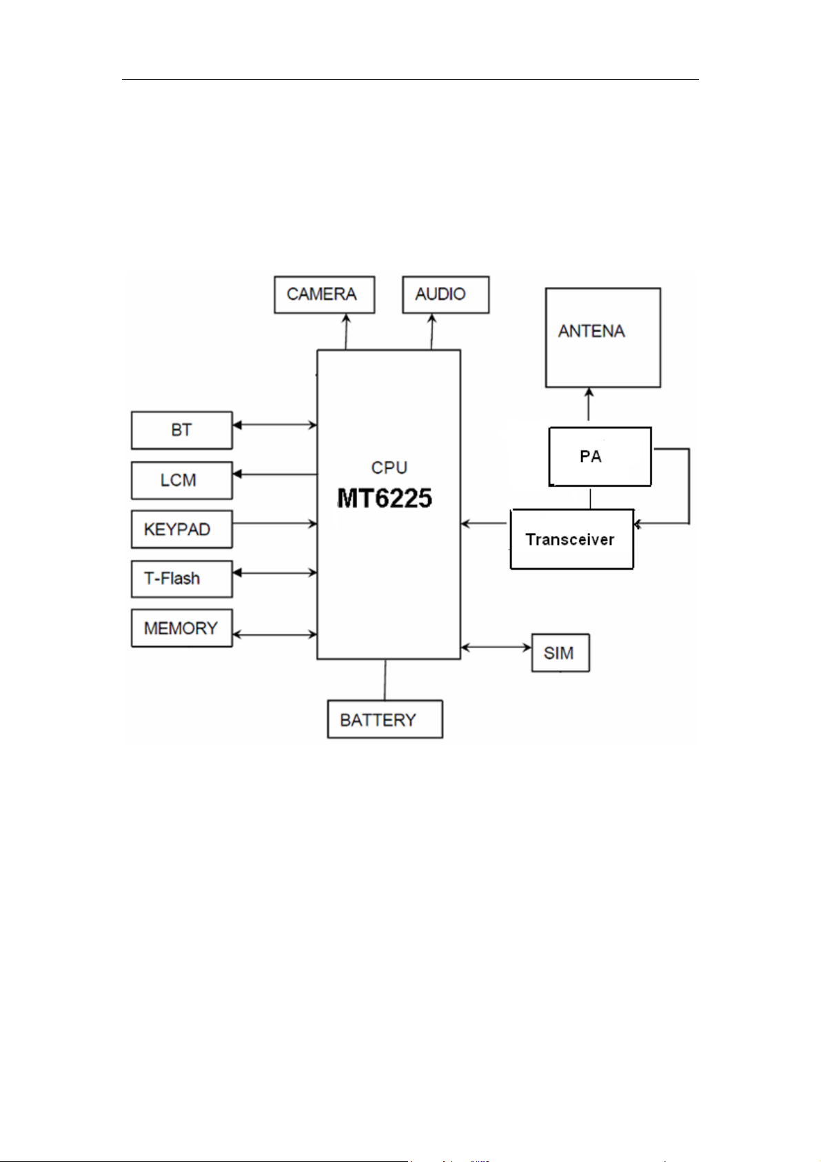
1 Overview DS185
1.1 About DS185 Phone
DS185 mainboard is designed based on the MTK platform, supporting two-frequency
communications. The mainboard also supports multimedia functions, such as MP4, MP3,
0.3m/pixels camera, USB and FM radio. The mainboard system consists of the base-band
(MT6225, the RF part (MT6139) and the Power management unit (MT6305).
DS185 system diagram
1
Page 4
DS185 Service manual
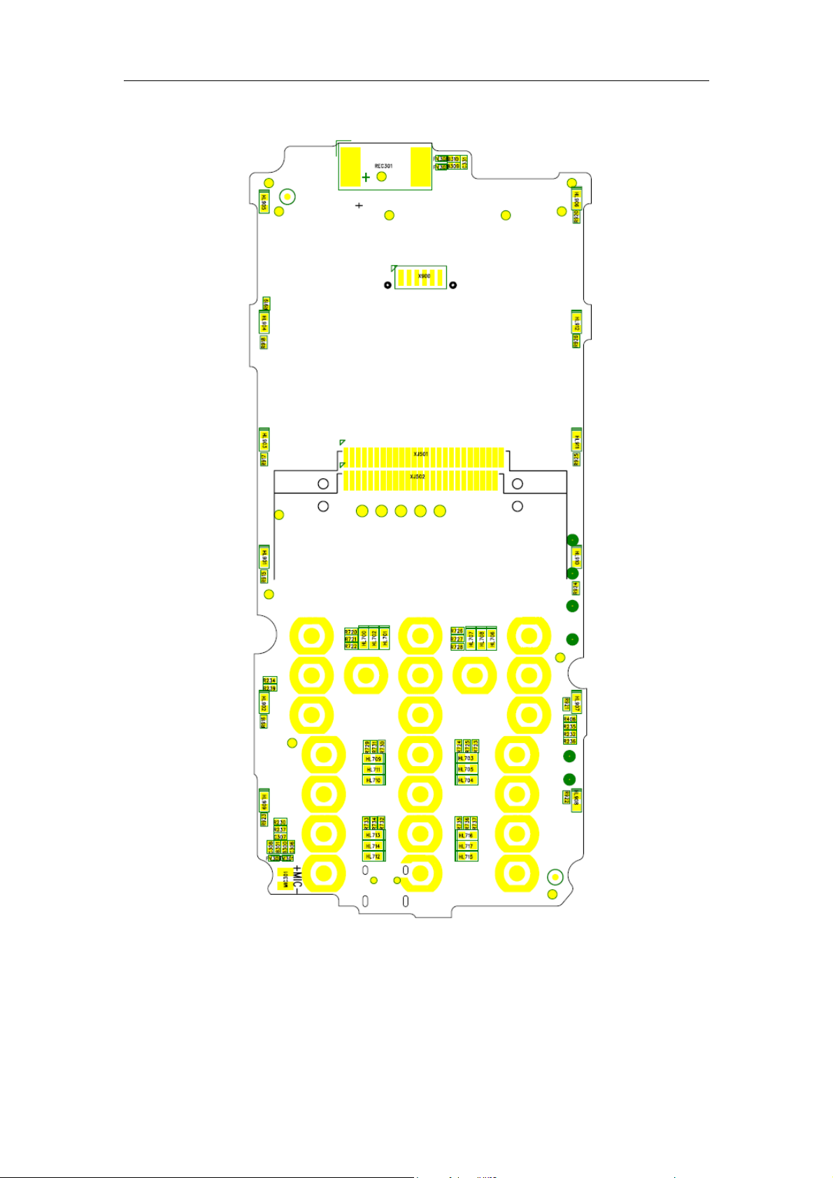
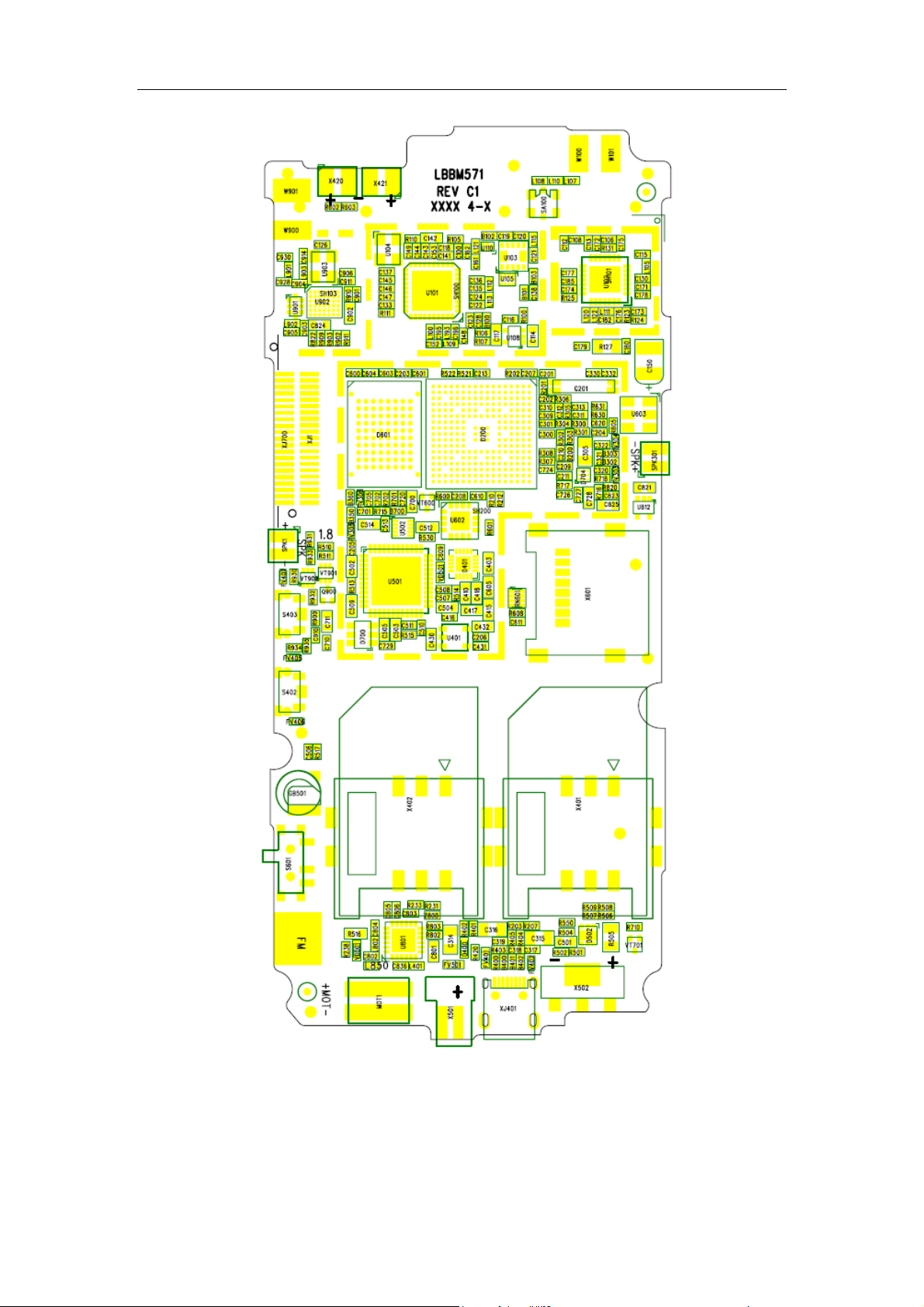
1.2 Distribution of the mainboard components
2
Page 5
DS185 Service manual
3
Page 6
DS185 Service manual
Name Model Location
MTK BB MT6225A/BGC-L D200
MTK PMU MT6305BN/CY-D-L // MT6305BN(CY-D-L) U501
Touch Screen Controller TSC2046IRGVR U602
NOR+PSRAM(128Mb+32Mb,1.8V) K5L2833ATA-AF66 D601
Bluetooth BC313141A18-IXF-E4 U902
Bluetooth filters DBF81F116-CSR-T U901
Dual SIM Card Controller MT6302N D401
Backlight Driver IC (4-way common
cathode)
RF Amplifier AX502 U102
RF front-end switch (tri-band) LMSP33CA-465 U103
FM AR1010-S85QFG*0 U801
LDO(2.8V, 300mA) RT9193-28PU5//RP1202-28PU5 U108,U812
LDO(3.3V, 300mA) EUP7967A-33VIR1 U401
LDO(1.8V, 2.8V, dual 150mA) PAM3102-AST26R1 D700
Stereo audio amplifier A7013M D704
Orientation sensor RPI-1031 U603
AAT3104IJQ-2-T1 U502
4
Page 7
DS185 Service manual
2 Signal flow and fault analysis
2.1 RF
2.1.1 RF diagrams
X190 mainboard adopts the plan of MTK MT6139.
RF part mainly consists of transceiver MT6139 (adopts program of near-zero IF receiver,
supporting the GSM / EGSM / DCS / PCS and 26M VCTCXO as the clock input,
integrated clock buffer, LO VCO and TX VCO and regulator, only need for external
connections of VBAT / AVDD). It uses Dual-band transmitter module AX502 (it supports
GSM / DCS / and integrated power control).
Function:
1. PA(AX502)supports EGSM / DCS / PCS and integrated FEM and automatic power
control which adopts voltage control to achieve and its role is to amplify the signal power
in accordance with the requirements. It is divided to two different power levels through
VRAMP signal. The transmit signal of GSM is 5 to 19, power is from 3.2MW to 2W while
DCS is 0 ~ 15, power from 1MW ~ 1W. PA is time-sharing work controlled by TX-EN chip,
the output power of PA is controlled by VRAMP (APC) through the voltage. PA is
intermittent work, by the BS to achieve the choice of frequency bands. Front-end module
FEM is the selection switch to select RX/TX and GSM/DC BAND, to increase the isolation
and prevent crosstalk between signals.
2. Transceiver (MT6139) has the RF modulation and demodulation, frequency synthesis
and clock buffering functions, that is to convert high-frequency to low-frequency and
low-frequency converted into high-frequency.
a. Transmit: MIC - MT6225 - MT6139 – PA - ANT
b. Receive: Antenna RX – FEM - SAW filter - MT6139 - CPU
A
N
T
PA
Ax502
Transceiver
MT6139
RF diagram
CPU
MT6225
5
Page 8
DS185 Service manual
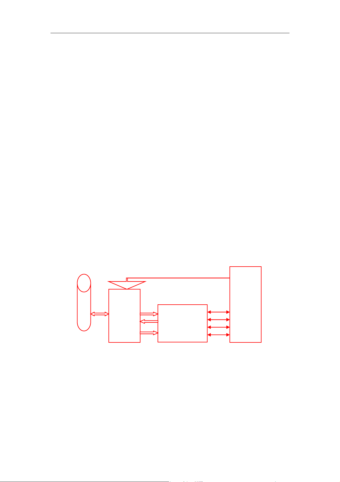
MT6139 MT6225
GSM RF and BB interface diagram
2.1.2 RF transmit signal flow
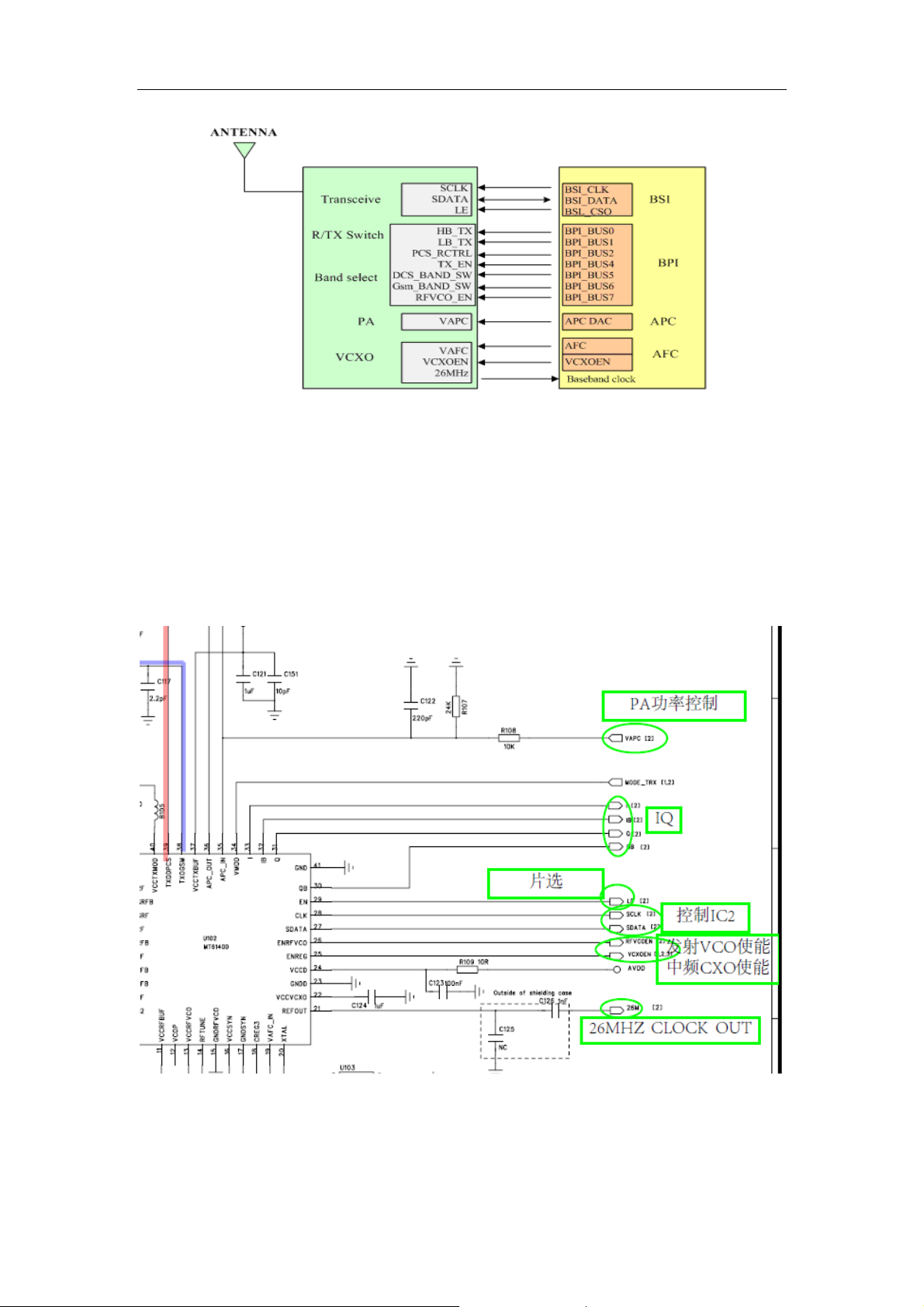
z Transmit Circuit
TX is composed of the modulation loop, power amplifier and antenna switch. PLL is
mainly in the internal MT6139, I / Q signal first enters into the MT6139, after entering the
TXVCO, the signal is modulated to RF, and then it outputs from the chip to PA(AX502),
converts into electromagnetic energy through antenna by the antenna switch after
enlarged. Build PI-type attenuation resistor networks from the MT6139 to PA. Antenna
switch to select RX, TX , as well as GSM, DCS.
z Maintenance Flow
z Maintenance preparation
Test conditions 1:Vbatt=3.8v~4.2v
6
Page 9
DS185 Service manual
p
k
Test conditions 2: GSM Band
Tx Mode CH62 Freq=902 4MHz Power Level:5
Test conditions 3: DCS Band
Tx Mode CH700 Freq=1747 8MHz Power Level:0
Test Equipment: CMU60100, Oscilloscope, Spectrum analyzer
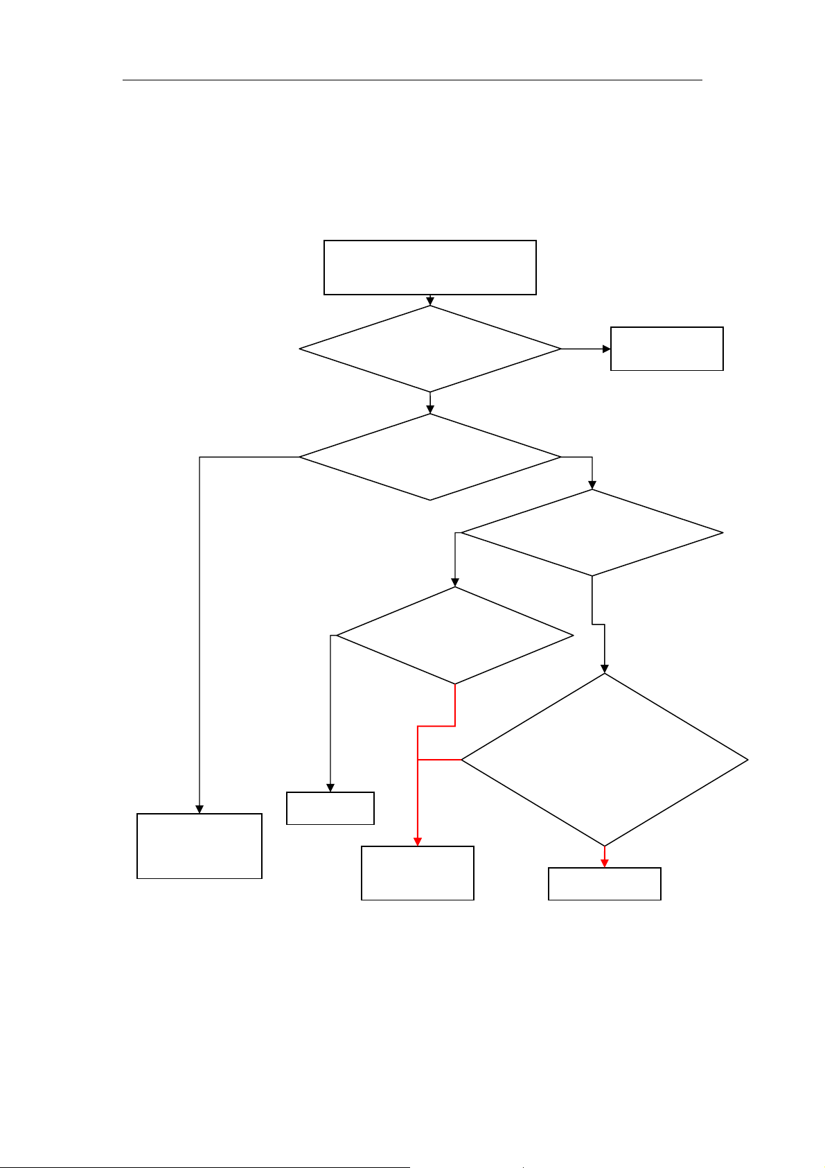
z Detection and Maintenance Flow Chart
(No transmit) Connect PC and cell
phone with maintenance of line, use
the Repair software making mobile
hone access to transmit state.
Y
Chec
whether there is IQ
signal?
Transceiver,
Y
Check PA output,
whether there is any RF
signal?
VBAT, PA_EN,
BANDSW_DCS, VAPC,
are they OK?
Y
N
N
N
Check CPU
N
Check Transceiver,
whether there is any RF
output signal?
Y
N
Check Transceiver
LE 、 SCLK/SDATA 、
RFVCOEN 、 VCXOEN,
are there correct signal?
Replace PA
Check RF switch or
matching network
Check CPU
Replace Transceiver
Y
z The maintenance process of Transmit malfunction
Use the Repair software making mobile phone access to transmit state. Choose 62CH in
GSM band, POWER Level for 5, DCS for 700CH, POWER Level for 0. Then, first observe
whether the current rises, and use the spectrum analyzer and oscilloscope to observe the
signal given in the above-mentioned flow chart, the specific signal waveforms shown as
below:
7
Page 10
DS185 Service manual
IQ signal waveforms of transceiver in transmit state:
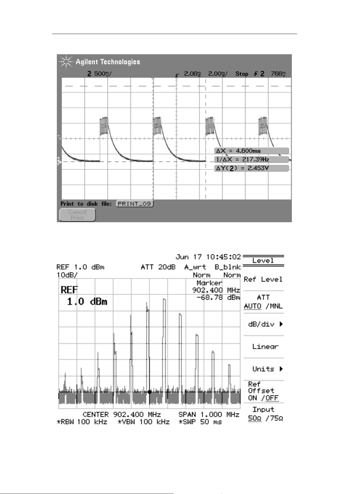
3.10 I/Q
RF interface spectrum analyzer is as follows:
GSM transmit signal
8
Page 11
DS185 Service manual
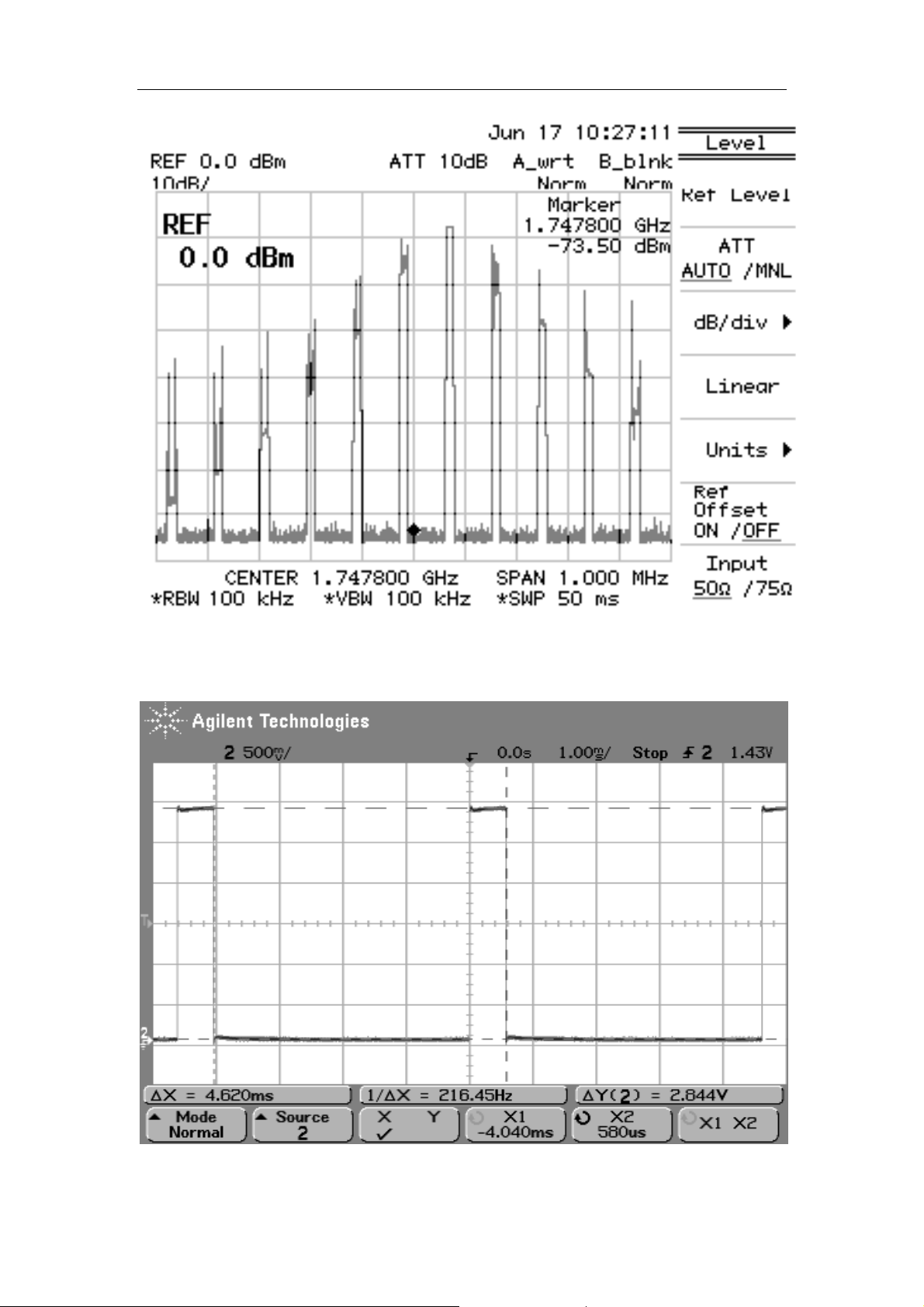
DCS transmit signal
PA-EN waveforms of PA in transmit state:
PA-EN
9
Page 12

DS185 Service manual
PA. BAND-SW waveforms:
PA.BAND-SW (GSM)
PA.BAND-SW (DCS)
10
Page 13

DS185 Service manual
PA Vramp waveforms:
Vramp (pcl5)
Vramp (pcl 19)
11
Page 14

DS185 Service manual
2.1.3 RF receive signal flow
z Receive Circuit
Antenna RX - antenna matching circuit - SAW filter - MT6139 (RX_VCO mixer band-pass - Amplification - RX_VCO mixer - filter - CPU
z Maintenance Flow
z Maintenance preparation
Test conditions
Test condition 1: Vbatt=3.8v~4.2v
Test condition 2: GSM Band
Rx Mode CH62=947.4MHZ Input power:-60dbm
Test condition3: DCS Band
Rx Mode CH698=1842.4MHZ Input power:-60dbm
z Detection and Maintenance Flow Chart
12
Page 15

DS185 Service manual
g
g
No Receive
Open Repair Software to connect PC with mobile phone, make
the phone access to receiving state, adjust signal generator to
corresponding CH, and connect the signal line to phone’s
RX SW.
N
Check CPU
N
Check CPU
Y
Y
Are Transceiver
SDATA、 SCLK 、
LE、RFVCOEN all
correct?
whether there is IQ signal?
whether there is any input
si
Y
Whether the voltage
Transceiver used is
normal? Is 26MHz
normal?
N
nal?
N
Check whether there is
any signal between PA
and ANT?
N
Whether PA signal
input pin has
received any
nal?
si
Y
Check whether there is
any signal between PA
and Transceiver?
Check the
corresponding power
supply and circuits of
26MHZ.
Y
Replace Transceiver
z The maintenance process of Receive malfunction
Maintenance process of NO Receive: Use Repair software to make mobile phone access
to pure receive state → Choose 62CH, Rx Mode CH62=947.4MHZ, Input power:-60dbm
in GSM frequency bands → Choose 698CH, Rx Mode CH698=1842.4MHZ, Input
power:-60dbm in DCS frequency bands → Adjust signal generator to corresponding CH,
connect the signal line to Cable of RF → Measure the related key signal by using
Spectrum analyzer and Oscilloscope → Measure the signal output pin of Transceiver,
whether there is any correct IQ signal output to CPU → Y: Check CPU (MT6225) / N:
Check Transceiver input pin, whether there is any corresponding CH input signal (Y:
Check whether Transceiver has correctly control the signal → Check whether the voltage
13
Page 16

DS185 Service manual
supply is normal → if normal, Transceiver can be judged of damaged / N: Check CPU,PA,
the paths ahead )
Signal waveforms refer to the following:
Output signal of Signal generator (Input):
GSM CH62 channel receives the signal
DCS CH 698 channel receives the signal
IQ signal output pin of Transceiver the state of receiving IQ signal:
14
Page 17
DS185 Service manual
Testing pin 26 AVDD voltage should be 2.8V, the signal Transceiver received from CPU
used to access the internal register of Transceiver. The corresponding waveform is as
follows:
15
Page 18

DS185 Service manual
3W(SDATA)
3W(SCLK)
16
Page 19

DS185 Service manual
3W(SCLK)
26M clock (can be measured by using the ACCoupling)
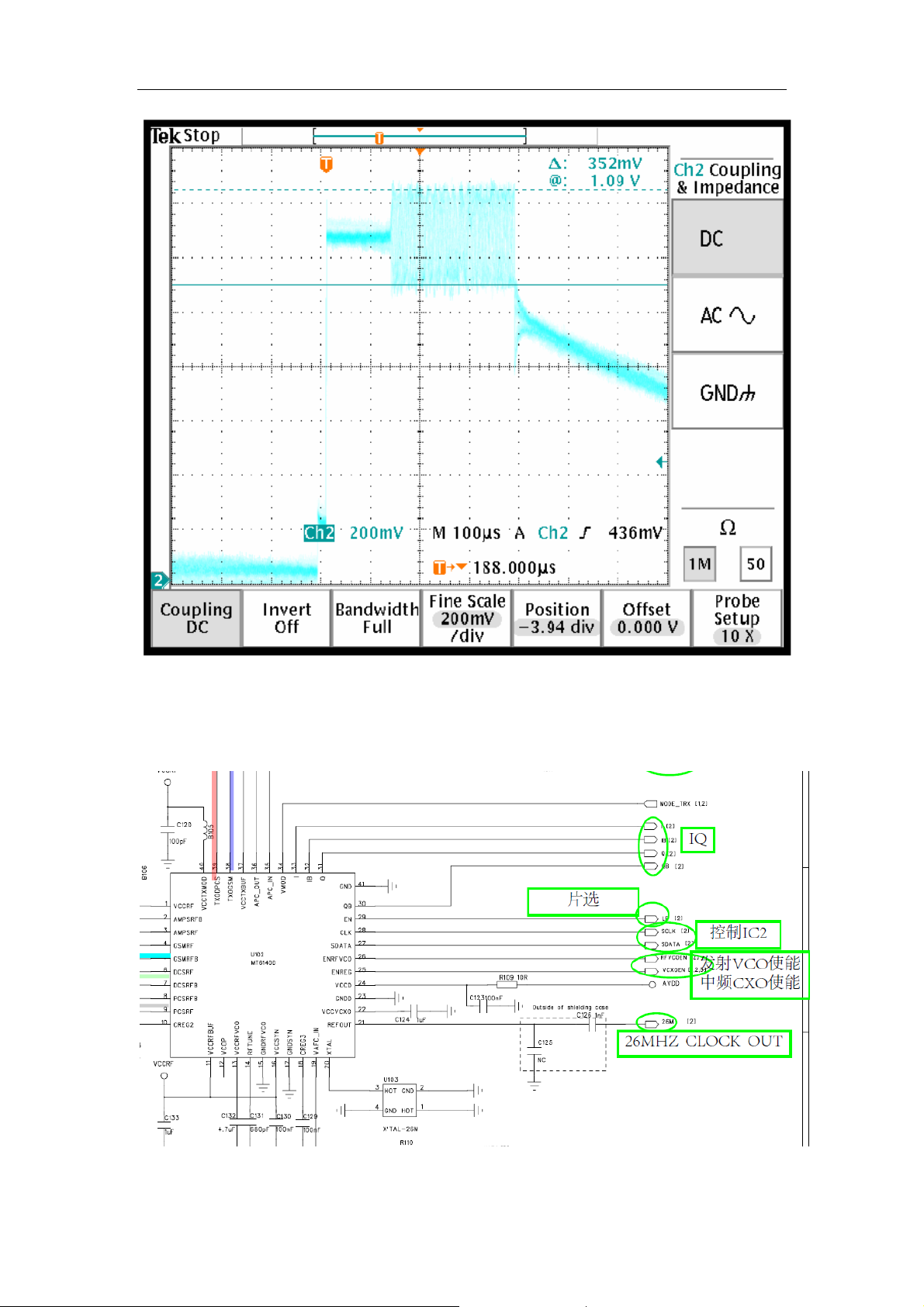
The AFC (automatic frequency control) from CPU to the crystal oscillator makes crystal
oscillator output accurate 26MHZ to Transceiver.
17
Page 20

DS185 Service manual
VAFC
TCXO output(26MHZ)
18
Page 21

DS185 Service manual
2.2 Baseband
2.2.1 Baseband diagrams
MT6305
DS185 Baseband consists of MT6225 and MT6305. MT6225 baseband, the core device
of the mainboard, is responsible for the normal work among various parts of mainboard,
such as voice processing, image processing as well as and MS communications.
MT6225 digital baseband contains 32-bit ARM7EJ-STM core and 84Kbyte SRAM.
MT6225 which is an Enhanced GSM Processor integrated Channel Codec subsystems
interiorly including Channel Codec, Intertlace / Deinterleave, Encryption / Decryption and
Control Processor subsystems including ARM7EJS and its peripheral circuits. There are
25 address lines,16 data lines, provided 4~10 external interrupt interface, 26M/52M/104M
operational clock, supports burst/page Nor Flash, USB1.1 interface, 64 chord, Nand falsh,
MMC/SD/MS/MS Pro. Multimedia memory, 2M CAMERA, JAVA accelerator, MMS, Irda.
Analog baseband contains MT6225 analog baseband chip, audio and baseband
codec.Three major functional blocks integrated internal: Audio codec including Voice input
/ Output channel, Buzzer output; Baseband codec including Differential I, Q input / output,
GMSK modulation and A / D, D / A; Auxiliary parts including AFC DAC, RAMP DAC, AGC
DAC and a seven-channel A / D. And WATCHDOG interface is set internal to enhance the
19
Page 22

DS185 Service manual
stability of the system.
MT6305 is an integrated power management chip, supply power for most of the device of
the mainboard. It consists of 600mW class AB single channel audio amplifie, backlight
LED driver and RGB LED driver, providing 11 LDO, as well as battery charging
management.
2.2.2 Power management
Power management consists of the charging circuit integrated in MT6305 and the external
charging circuit. In addition to complete the logic level conversion of SIM card and putout
the system reset signal.
z Charging circuit
z Power system
VCORE = 1.2V, VADD = 2.8V (to ensure MT6139 make 26MHZ buffered output normally)
VRTC = 1.2V (real-time clock voltage)
PMIC_VTCXO = 2.8V (Its function is to provide power and the signal type conversion, as
well as charging.)
20
Page 23

DS185 Service manual
Power key
Hold or wake-up key
Charging circuit
SIM Interface
Circuit
System
Reset
LDO power
output
21
Page 24
DS185 Service manual
Boot process:
The normal boot is to press boot key which is that the PWRKEY is being dragged down.
Once the boot key is pressed, all LDO are open expect VISM. After VCORE opening
RESET timer and timer out, RESET is being pitched up to start the digital baseband chip,
that is, MT6225 starts to run and roll polling MT6305’s ROWX pin, pitch up its PWRONIN
pin, then you can release the boot key. This is the initial boot process.
2.2.3 Minimum System part
z MCU (U100)
MT6225 for mBGA package, integrates the following seven modules:
Baseband receiver: Baseband A /D conversion of I/Q signals.
Baseband transmitter: Baseband D/A conversion of I/Q signal and signal smoothing.
RF control: 2 DAC converters for automatic power control and automatic frequency
control.
Auxiliary ADC: Monitoring battery and other analog functions.
Audio: Provides a complete analog audio signal processing, including micphone
amplifier, A/D and D/A converter, headphone drivers and so on.
Clock generator: a clock square wave map system clock, three phase-locked loop
offer clock for MCU, DSP, USB modules.
32K Crystal: 32KHz crystal oscillator circuit used for the RTC.
22
Page 25

DS185 Service manual
z NAND FLASH compatible with SDRAM
The mobile phone designed of compatible with NAND FLASH and SDRAM pad
considering the different customers, so it can be achieved by soldering different chips.
23
Page 26
DS185 Service manual
Flash memory
data cable
SDRAM
Data cable
SDRAM
Clock signal
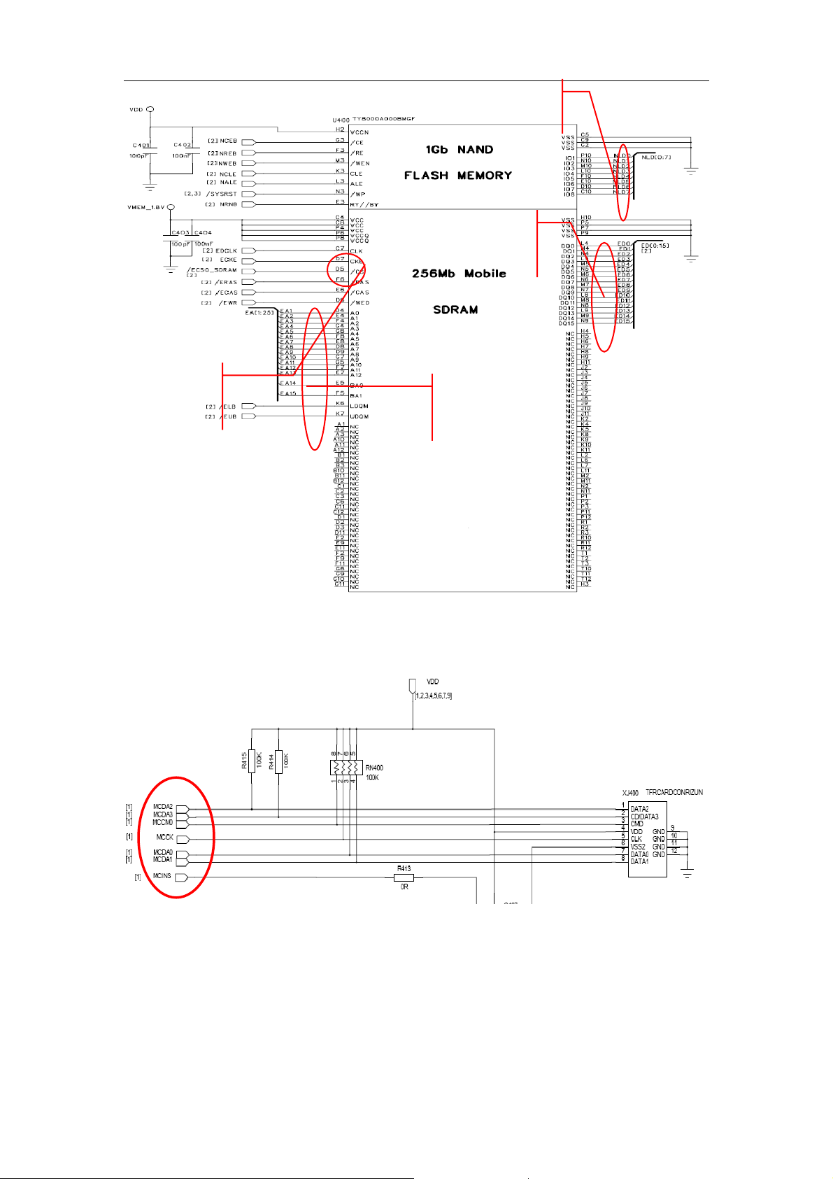
z T-Flash card
MCDA0~3 is SD (or memory) serial data I/O, MCCK is SD (or memory) serial clock,
MCCM0 is SD command output / memory.
SDRAM
Address
cable
2.2.4 Audio Frequency
z Audio Power Circuit
The mobile phone uses a professional high-fidelity digital stereo power amplifier for audio
amplification. And the MP3_OUT are the audio signal decoding from the CPU, not just
mp3 signal. AUDIO_PWR is the amplifier input power signal, PIN5 (SHDN) is the enable
signal, usually need to amplify when Q501 turn down; SPK signal is the amplified output
audio signal.
24
Page 27

DS185 Service manual
25
Page 28

DS185 Service manual
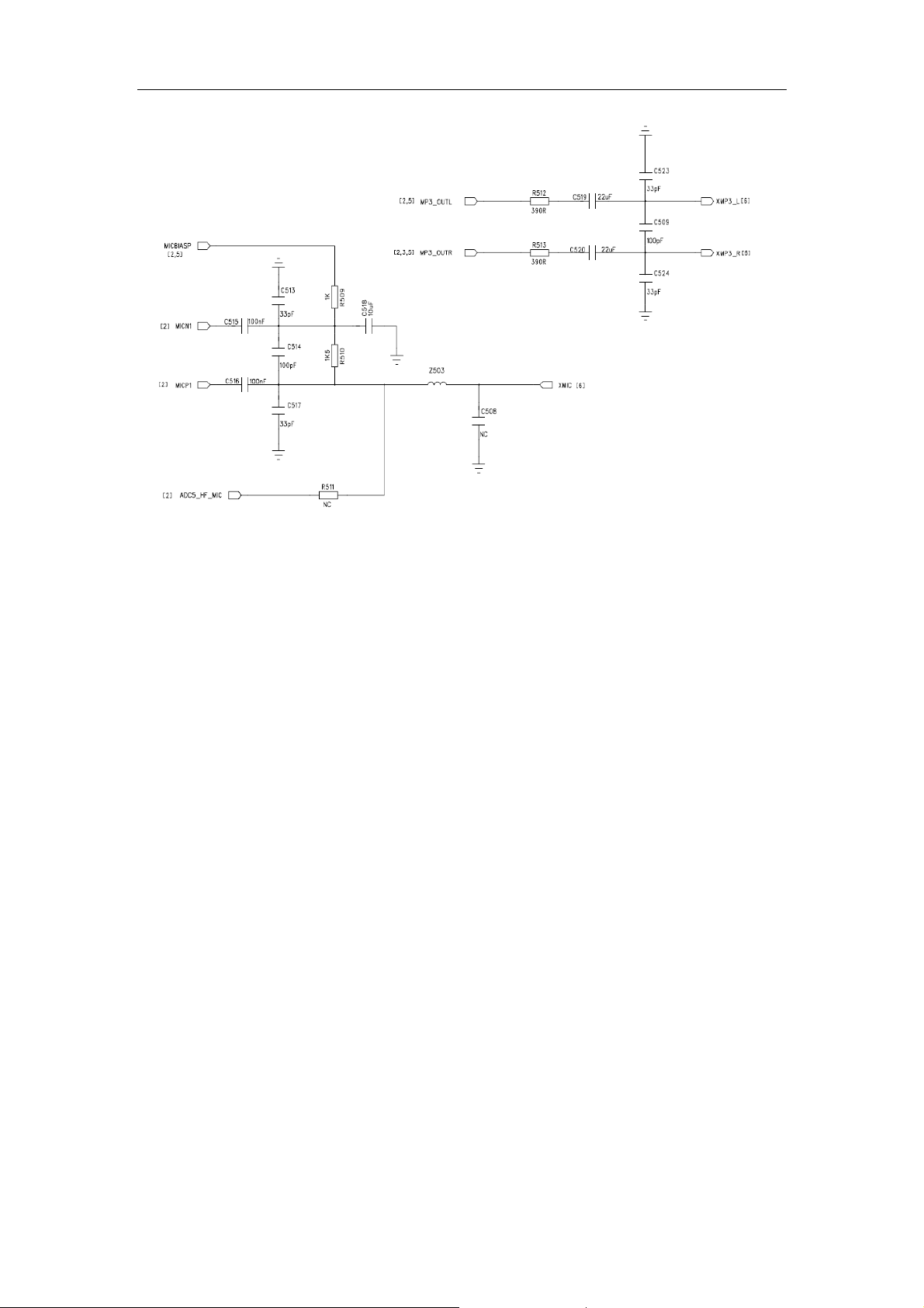
z MIC, RECEIVER loop
Check basic offset voltage signal of MICBIASP and MICBIASN and the language signal
MIC itself when the MIC is good but no response of LOOP MIC in test.
z Earphone loop
Earphone loop includes headset speaker and MIC two-way signal. Check the circuit
access situation when there is something abnormal (such as: no sound in headset
speaker, Mic invalid, etc.) after inserting the earphone while the headset accessories are
good.
MIC bias voltage
MIC bias voltage
26
Page 29
DS185 Service manual
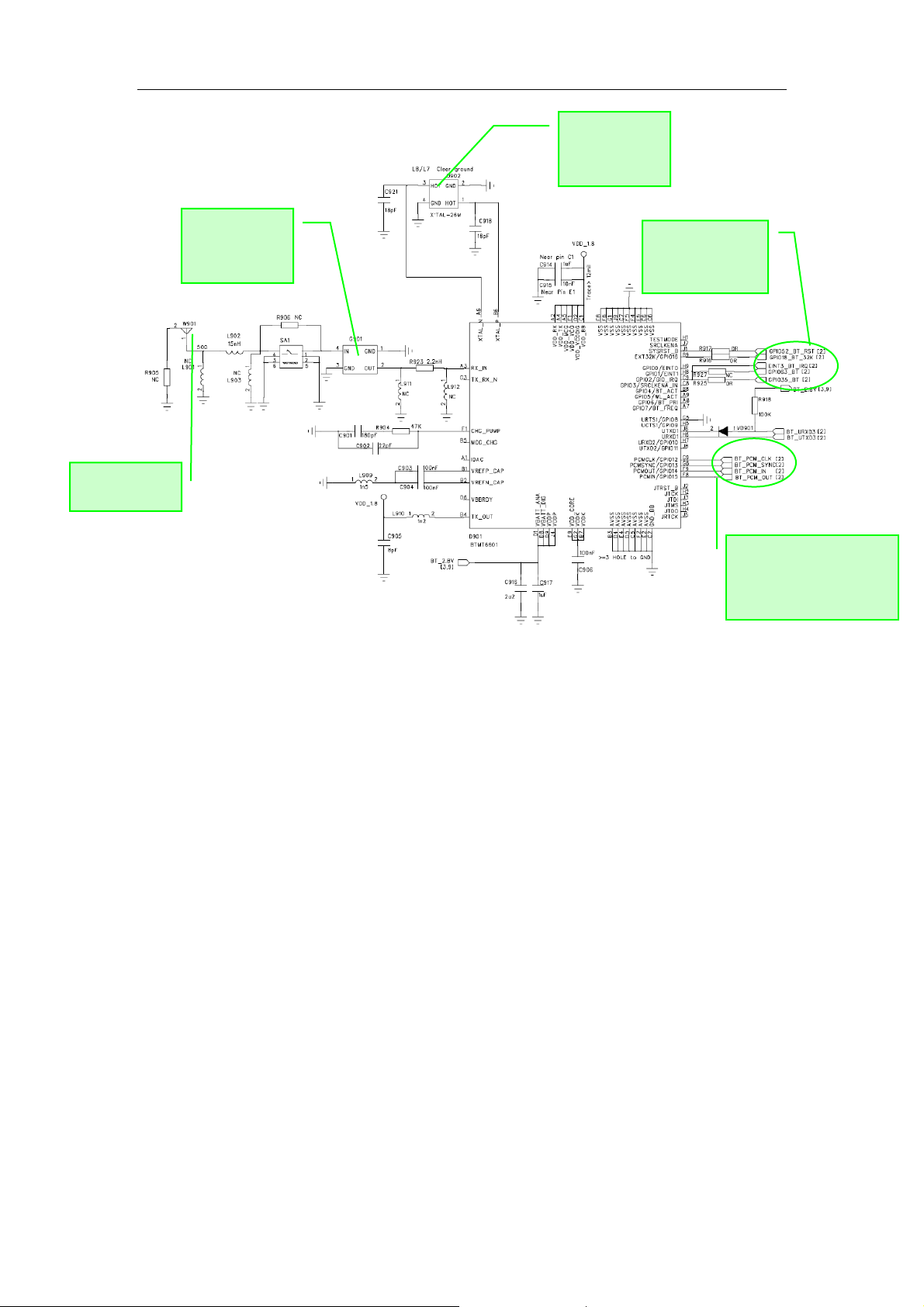
2.2.5 Bluetooth
z Bluetooth
Bluetooth works in a 2.4GHz GSM and use ISM (industrial, scientific, medical) band in
order to ensure that the Bluetooth can be used in worldwide. Bluetooth antenna
transmission power comply with the requirements of FCC regarding the ISM band
0dBm.The maximum hopping rate of system is 1600 hop / sec, and in between the
2.402GHz to 2.480GHz,using 79 1MHz bandwidth 79 frequency. Communication dist ance
designed by system is 10 meters (0db).If you increase the transmitting power (20db), this
distance can reach 100 meters. With time-division manner in full-duplex communication
(TDD), transfer rate is designed to 1MHz.Use of Forward Error Correction (FEC) coding
techniques to reduce the random noise when transmitting in the long-distance.Use a
strong anti-fading continuously variable slope modulation (CVSD) coding method to
improve the quality of voice and use frequency modulation method to reduce the
complexity of equipment.
z Bluetooth Principle
The native Bluetooth functionality is achieved through BC313141A18 chip. The digital
information is converted to wireless signal accord with Bluetooth agreement to transmit
information. At the same time, the information received is converted to the digital
information mobile which phone system can identify. It is composed of antenna, system
clock crystal and BC313141A18 chip.
27
Page 30
DS185 Service manual
Bluetooth
antenna
2.45G
band-pass
filter
Bluetooth
clock signal,
the crystal
System signal;
32KHZ clock
signal
Bluetooth and system
data cable; using
digital pulse code
2.2.6 Baseband common malfunction
z NOR Flash programming does not download
Data lines used for downloading software: VBA T, TX, RX, GND, CHARGE. It is mostly due
to the false solder and wire bonding. First check whether the serial port of PC and cell
phone is unrestricted, if not, it is caused by being lack of devices or empty solder of power
manager, USB-con and peripheral resistance. Measure the TX, RX signals by using
AC-coupled oscilloscope to track the signal flow, if a certain period circuit of no signal it
may be AC short circuit to ground, or is caused by a short circuit and open circuit. On
checking the malfunctions, first should carefully observed the welding of these devices
with a magnifying glass, then plug in the download line to observe whether the current is
normal, there is short-circuit to ground of VCHG or VBAT if the current is large, at this time
cut off power supply as soon as possible, and then find the short-circuit point; It may the
abnormal output power supply of a certain circuit that the current is greater than normal
(about 30 mA) but not particularly large, at this time should check whethe the valgate of
VCORE (1.8V), VDD (2.8V), VADD (2.8 V), VTCXO (2.8V), VRTC (1.5V), VMEM (2.8V) is
noamal, if not, bad welding can be detected. Focus on checking the welding of PUM and
USB-CON if there is little or no current. Unplug and re-plug the download line to see if it
caused by poor contact; It can be test that whether the output to the CPU of 26MHz clock
signal is normal by using oscilloscope.
z Detection and Maintenance Flow Chart of No download malfunction
28
Page 31

DS185 Service manual
Not download
Eliminate any
reasons for not
download except
the cell phone.
Check whether the
system connector is
false soldered or
damaged.
Yes
NO
Check whether it is the problems
of allocation of procedure,
download cable, power supply,
software, PC phone.
Check whether the serial port of
PC and cell phone is unrestricted.
NO
Check the RC between
system connector and
CPU, and the ESD.
Connected to the download line
and observe the ammeter whether
it is high-current (normal current
is generally about 30mA).
Little or no current
Check whether the voltage supply of CPU
power manager, PMU and LDO is normal,
whether there is any power supply open circuit.
NO
Yes
Yes
Normal current but no download
Check VCORE 、 VDD 、 VA DD 、
VTCXO、VRTC、VMEM、measure the
clock signals of 26MHZ、32KHZ
Quickly disconnect the
connection, and touch
the chip gently to see if
it is hot, if no focus on
measuring the
short-circuit point by
using multimeter.
Check whether CUP, NAN FLASH
and SDRAM is OK, LDO is normal?
z Analysis of the keyboard
Keyboard circuit uses scanning detection method. When button is pressed, the scan
signal detects the corresponding row, column, and then the system software identify the
key functions.
29
Page 32

DS185 Service manual
z All the keys fail after the phone power on
A、Check outer exclusion of the connector and the varistor, whether there is short-circuit.
B、Check the connector if there is short-circuit while welding.
z One key fail
Check whether there is dirty under the DOME key. If the problem persists, check whether
the circuit is breaking.
z A few keys fail
Focus on checking whether there is open-circuit, cold solder joint of interface circuit and
the resistance disconnected.
z LCM circuit analysis
LCD data
LCD control
signal
Backlight
control signal
z The signal waveform
30
Page 33

DS185 Service manual
Chip select signals CS:
Screen reset signal LRST:
Screen Write signal LWR:
31
Page 34

DS185 Service manual
About the screen, first find the problem whether is mainboard or screen by adopting
replacement method, then focus on checking the LCM-CON welding and measuring the
input voltage VBAT, and enable control signal.
Note: The waveforms may be different according to the settings and different devices in
maintaining.
32
Page 35

DS185 Service manual
33
 Loading...