

Page 1

956A-201-M2 & 897A-2XX
Area Monitoring System
Instruction Manual
Page 2

(Blank page)
Page 3

CONTENTS
Section 1: GENERAL INFORMATION........................................................ 1-1
1.1 Product Specification ................................................................................... 1-1
1.2 Specifications, G-M Detector, Model 897A Series ....................................... 1-3
1.3 Specifications, G-M Detector Check Source, Model 897A Series................ 1-4
1.4 Specifications, Detector Preamplifier (Integral)............................................ 1-4
1.5 Detector Part Number Description ............................................................... 1-5
1.6 Readout Part Number Description ............................................................... 1-6
1.7 Universal Digital Ratemeter, Model 956A-201-M2....................................... 1-7
1.8 Application ................................................................................................... 1-8
1.9 Specifications Model, 956A-201-M2 ............................................................ 1-9
1.10 Auxiliary Equipment ................................................................................... 1-10
1.11 956A-201-M2 Modifications ....................................................................... 1-11
1.12 Recommended Spares .............................................................................. 1-12
1.13 Receiving Inspection.................................................................................. 1-12
1.14 Storage ...................................................................................................... 1-13
Section 2: OPERATION .............................................................................. 2-1
2.1 Installation.................................................................................................... 2-1
2.2 G-M Detector Mounting................................................................................ 2-1
2.3 G-M Detector Setup..................................................................................... 2-1
2.4 UDR Mounting ............................................................................................. 2-2
2.5 Electrical Interface ....................................................................................... 2-3
2.6 Setup ........................................................................................................... 2-6
Section 3: THEORY OF OPERATION ........................................................ 3-1
3.1 Operation ..................................................................................................... 3-1
3.2 Detector Operation, Model 897A-2XX.......................................................... 3-1
3.3 UDR Operation, Model 956A-201-M2.......................................................... 3-2
3.4 Operational Modes ...................................................................................... 3-4
3.5 Alarms.......................................................................................................... 3-7
3.6 Jumper Selectable Configuration Functions .............................................. 3-10
3.7 Power Up Procedure ................................................................................. 3-12
3.8 UDR Function Switch and Parameter Entry............................................... 3-13
3.9 Setpoint Descriptions................................................................................. 3-15
3.10 Setpoint Error Codes ................................................................................. 3-16
3.11 Analog Output............................................................................................ 3-17
3.12 Software Calculations ................................................................................ 3-18
3.13 Functional Description, Model 897A G-M Detector.................................... 3-19
3.14 Functional Description Universal Digital Ratemeter (URD), Model 956A-
201............................................................................................................. 3-21
i
Page 4

Section 4: MAINTENANCE AND CALIBRATION....................................... 4-1
4.1 Maintenance ................................................................................................ 4-1
4.2 Calibration.................................................................................................... 4-1
4.3 Calibration/Electronic Adjustment ................................................................ 4-1
4.4 955A System Field Calibration..................................................................... 4-3
4.5 Detector Calibration ..................................................................................... 4-5
Section 5: TROUBLESHOOTING ............................................................... 5-1
5.1 Troubleshooting ........................................................................................... 5-1
5.2 HV Power Supply Adjustment...................................................................... 5-7
Appendix A: CONNECTOR DESIGNATIONS ................................................A-1
A.1 Connector Designations............................................................................... A-1
Appendix B: APPLICABLE DRAWINGS........................................................B-1
B.1 Applicable Drawings ....................................................................................B-1
Appendix C: BILL OF MATERIALS................................................................C-1
C.1 Bill of Materials ............................................................................................C-1
Appendix D: COAXIAL CABLE TERMINATION INSTRUCTIONS ................ D-1
D.1 Coaxial Cable Termination Instructions ....................................................... D-1
Appendix E: SUPPLEMENTAL DATA (CUSTOMER SPECIFIC).................. E-1
E.1 Supplemental Data (Customer Specific) ...................................................... E-1
ii
Page 5

SECTION 1
GENERAL
INFORMATION
1.1 PRODUCT SPECIFICATION
The Victoreen Model 956A-201-M2 Digital Ratemeter, when operated in conjunction with an 897A-2XX
G-M detector, is a single-channel area radiation monitoring system capable of operating over the ranges
of 0.01 to 10
monitors gamma radiation over a 5-decade range and provides indication when the radiation level
decreases below a fail threshold, exceeds a warn setpoint, exceeds a high setpoint, or exceeds an over
range setpoint. The over range feature provides two significant benefits. First, it prevents the system
from displaying an on-scale, but inaccurate, reading should the detector become saturated. Second, it
lessens the risk of damaging the detector by disabling it during an overrange condition. Relay outputs are
available to activate alarm annunciators. Analog outputs are available for trend display on a strip chart
recorder or computer. In addition, the monitoring system has an integral check source to verify
operational integrity. The system consists of a Model 897A Series Geiger-Mueller (G-M) Tube Detector
with integral preamplifier and the Model 956A-201-M2 Universal Digital Ratemeter (UDR). A more
detailed description of each piece of equipment can be found in the following paragraphs.
3
mR/h, 0.1 to 104 mR/h, or 1 to 105 mR/h, depending on the detector selected. The system
The Model 956A-201-M2 is a modified version of the standard Model 956A-201. The modification
consists of adding the Optional 0-10mV analog output, a “Trip Test” function, and 120 Vac powered,
FAIL and HIGH Alarm outputs (connector P2) to operate a locally mounted alarm.
The 0-10mV analog output is provided by installing the P/N 942-200-95-M1 Dual Analog Output option
circuit board. The 0-10mV output is wired to UDR P6-7/8. The 0-5v output is not used, and is not wired
out to the rear panel.
The “Trip Test” function is provided by replacing the front panel with the P/N 956A-201-20M2 front panel.
The modified front panel adds switch SW5, to actuate the “Trip Test” function. The standard EPROM is
also replaced with P/N 94095605 EPROM. When the “Trip Test” pushbutton is depressed, the alarm
relays will trip, the analog outputs will be driven upscale, the bargraph is driven upscale, the units
backlights are illuminated, the alarm LEDs illuminate, the check source LED illuminates, and the digital
display is forced to display 8.8.8.8.8. Releasing the pushbutton returns all functions except the alarms to
normal. The alarm LEDs and bargraph are returned to normal by pressing the Acknowledge pushbutton.
The 120 Vac powered FAIL and HIGH Alarm outputs (connector P2) are implemented via internal wiring
modifications in the UDR. The FAIL alarm output is obtained by operating the Auxiliary Relay, K1, in
parallel with the normal Fail relay, K3. The HIGH alarm output is obtained from the HIGH alarm relay, K5.
Refer to Modification Sheet 956A-201-M2MS for additional information on the modification.
1-1
Page 6

The Model 956A-201 Series Readout and 897A Series G-M detectors have been successfully subjected
to seismic and environmental qualification testing per IEEE 344-1975 and IEEE-323-1983. In addition,
EMI/RFI testing per the requirements of EPRI TR-102323-R1, MIL-STD-461D, and EN 61000-6-1:2001
has also been successfully performed. Please consult the factory for specific details of the qualification
testing program.
The 956A-201-M2 operation described herein is based on the use of EPROM P/N 94095605, Rev. 1.
Geiger-Mueller Detector, Model 897A-Series
Victoreen 897A-Series G-M detectors use a thin walled Geiger-Mueller tube to detect ionizing radiation.
Each 897A-Series detector has a G-M tube, a check source, and a preamplifier. The check source is a
low-level radioactive source actuated by a + 15 Vdc meter movement. The preamplifier provides the
pulse conditioning and cable driving capability necessary to drive a Victoreen 956A-201 Series digital
ratemeter.
All 897A-Series detectors are functionally identical. They differ only in housing material, tube type, and
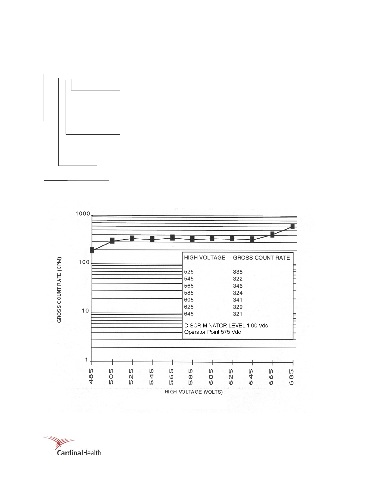
range. The 897A Series detectors operate in the voltage range of 500 - 650 Vdc. An example of the
detector plateau, based on different high voltages, is located in Figure 1-1. Refer to the specifications for
all 897A-Series G-M detectors for further information.
NOTE
The 897A Series G-M detectors contain an eight-microcurie 36CI
check source. Nuclear Regulatory Commission regulations
define this source as an exempt quantity.
Application
The Model 897A G-M Detector is designed to operate with the Victoreen Model 956A-201 Universal
Digital Ratemeter (UDR) or with other Victoreen readouts. Each detector measures a five-decade range.
Three measurement ranges are available: low, medium, and high. The low range covers 0.01 to 10
mR/h, the medium covers 0.1 to 10
4
mR/h, and the high covers 1 to 105 mR/h. The Model 897A detector
may also be used with the Victoreen Model 960 Digital Radiation Monitoring System equipment or the
Victoreen Model 856 Analog Readout.
3
1-2
Page 7
1.2 SPECIFICATIONS, G-M DETECTOR, MODEL 897A SERIES
Dimensions (Approximate 7 1/8 x 3 inches (18.1 x 7.6 cm)
Weight (Approximate) 2.5 lbs.
Housing Material
897A-210, 897A-220, 897A-230
897A-211, 897A-221, 897A-231
Fill Gas:
897A-210, 897A-211
897A-220, 897A-221
897A-230, 897A-231
G-M Tube Wall Thickness:
897A-210, 897A-211
897A-220, 897A-221
897A-230, 897A-231
Mounting Wall mount
Mating Connectors 897A-2x0:
Required Cable P/N 50-100 or substitute with two coaxial
External Pressure Limit 30 psig
Storage Temperature -10° to 122°F (-23° to 50°C)
Operating Temperature -10° to 122°F (-23° to 50°C)
Relative Humidity 0 to 95% non-condensing
Operating Voltage 500 – 650 Vdc (supplied by digital ratemeter)
Plateau Length 100 – 150 Vdc
Plateau Slope:
897A-210, 897A-211
897A-220, 897A-221
897A-230, 897A-231
Dead Time (Approximate)
897A-210, 897A-211
897A-220, 897A-221
897A-230, 897A-231
Detector Element Life Exceeds 1000 hours at full-scale
Energy Dependence of Reading +/- 15% from 80 keV to 1.5 MeV
Detector Accuracy ± 20% of actual dose for Cs-137
Radiation Detected Gamma rays, X-rays
Aluminum, weatherproof
Stainless Steel, weatherproof
Neon/Argon/Halogen
Helium/Neon/Halogen
Helium/Neon/Halogen
40 mg/cm
80 mg/cm
2
2
80 mg/cm2
92-7005-17A, 12 Pin Female
92-7005-12A, Bushing
92-7005-9A, Clamp
897A-2x1 (stainless steel):
92-7005-15A, 12 Pin Female (stainless steel)
92-7005-12A, Bushing
92-7005-13A, Bushing
conductors, two twisted pairs, and overall shield.
0.1%/V
0.2%V
0.3%V
45 microseconds
28 microseconds
20 microseconds
1-3
Page 8
1.3 SPECIFICATIONS, G-M DETECTOR CHECK SOURCE,
MODEL 897A SERIES
Radionuclide
Source Activity: 8 microcuries
Scale Reading (Approximate)
897A-210, 897A-211
897A-220, 897A-221
897A-230, 897A-231
Voltage 12 – 15 Vdc
Encapsulation Brass, high temperature soldered
36
CI
10-150 mR/h, Typical
10-50 mR/h, Typical
10-50 mR/h, Typical
1.4 SPECIFICATION, DETECTOR PREAMPLIFIER
(INTERGRAL)
Input Impedance >100 k-ohms
Output Impedance 50 ohms
Output Pulse Polarity Positive
Output Signal (50 ohm terminated) + 5 Vdc square-wave
Low Voltage* + 15 Vdc (Optional + 10 Vdc is Jumper Selectable)
Power Requirements + 15 Vdc @ 120 mA
Maximum Cable Length 2000 feet
Electronic Exposure Life Approximately 105 rads
Discriminator Level Adjustable from 0 to 1.5 Vdc (nominal value =1.00
Vdc)
Anti-Jam Level Adjustable from 0 to + 3 Vdc
Anti-Jam Oscillator Frequency Approximately 50 kHz
Pre-divide* Jumper Selectable
Analog & Digital Monitor Configuration Divide by 2, Square wave output
Optional Monitor Configuration Raw pulse output
* Preamplifier low voltage and pre-divide are selected with jumpers. Refer to the preamplifier circuit
description for more information. Standard Configuration is +15 Vdc Divide by 2.
1-4
Page 9

1.5 DETECTOR PART NUMBER DESCRIPTION
897A-2 XY
2 = High reliability components for Class 1E service
PRODUCT SERIES
897 = Sr-90 check source (NRC license required) with a
Y = 0, Aluminum Housing
Y = 1, Stainless Steel Housing
X = 1, 0.01 mR/h – 1E3 mR/h
X = 2, 0.10 mR/h – 1E4 mR/h
X = 3, 1.00 mR/h – 1E5 mR/h
120 VAC solenoid actuator. No longer manufactured.
897A = CI-36 check source (exempt quantity) with + 15
VDC meter movement actuator.
1-5
Page 10
1.6 READOUT PART NUMBER DESCRIPTION
956A-20X-MX
2 = High reliability components for Class 1E service
PRODUCT SERIES
956 = 16k x 8 PROM, 8k x 8 RAM; 128 bytes EEPROM; V-Channel front
Blank = Standard Unit
M = Special Options/Modifications
MX = Special Modification (X = Modification Number)
M2 = Add 942-200-95-MI Dual Analog Output Circuit Board, Trip Test
Function, and Externally Powered Fail and High Alarm Relay
Contacts
00 = 120 Vac Check Source Mechanical (Discontinued 9/95)
01 = 15 Vdc Check Source Mechanical (current product configuration)
0X = Future Variations
panel – No longer manufactured
956A = 32k x 8 PROM, 8k x 8 RAM, 256 bytes EEPROM; flat front panel –
revised rear panel pinouts.
Figure 1-1 Detector Plateau (typical)
1-6
Page 11

1.7 UNIVERSAL DIGITAL RATEMETER, MODEL 956A-201-M2
The Victoreen Model 956A-201-M2 is a modified version of the Model 956A-201 Universal Digital
Ratemeter (UDR), when connected to a Victoreen Model 897A-2XY Geiger-Mueller (G-M) tube detector,
comprises a monitoring system that operates over a five-decade range. The UDR provides display,
control, and annunciation functions for the monitoring system, and will display readings in the range of
0.01 to 10
Standard features for the instrument consist of a three-digit display of the radiation value, in units of
mR/h, R/h, or kR/h, and a multi-colored bargraph indicator that covers the entire range of the UDR. The
bargraph will change color in the event of an alarm condition (green for normal, amber for warning, and
red for high). Front panel alarm indicators and rear panel relay outputs for alarm annunciation are also
included. Front panel pushbuttons are provided to apply power, display alarm limit setpoints,
acknowledge alarms, and to activate the check source. In addition, the 956A-201-M2 is provided with a
front panel mounted TEST pushbutton, that performs a self-test of the UDR.
Analog outputs of 0 - 10 Vdc (1) and 4 - 20 mA (2) are provided for recording and computer monitoring.
The outputs may also be used to drive a remote meter or a local (i.e. near the detector) indicator.
In addition, the 956A-201-M2 is provided with the P/N 942-100-95-M1 dual analog output option circuit
board that provides a 0-10 mV dc analog output.
The 956A-201-M2 also included an internal wiring modification that applies 120 Vac to the Fail and Alarm
relay contacts. The auxiliary relay, K1, is hard wired to operate in parallel with the Fail relay to supply AC
power to a local alarm. AC power is supplied from rear panel connector P1 to detector connector P2.
Refer to Modification Sheet 956A-201-M2MS for additional information on the modification.
5
mR/h. Refer to Figure 1-2 for view of the 956A-201-M2 front panel.
All electronics required to interface with the VICTOREEN 897A Series G-M detector are included within
the 956A-201 UDR. The electronics consist of a high voltage power supply, low voltage DC power supply
and the hardware/software required for UDR operation. The system also includes an overrange indicator
to preclude the possibility of on-scale readings when the radiation field is beyond the range of the
detector.
The following paragraphs describe the available options. A separate manual for each option board is
available with more detailed information. Listed below are the option boards currently available.
1. 942-200-75: ANALOG INPUT OPTION BOARD - (Generally not used for normal operation with the
956A-201 UDR, however, it is used if the UDR is part of a simulator) Contains four (4) separate
channels for analog inputs. A 0 to 10 Vdc input or 4 to 20 mA input can be selected independently for
each channel using the jumpers and switches provided on the board. Possible inputs to the board
include: temperature, pressure, flow, or simulated radiation.
2. 942-200-80: COMMUNICATIONS LOOP OPTION BOARD - Designed to enable a EIA RS232C
standard communications link between VICTOREEN's ratemeter and a user computer system or CRT
terminal, with baud rates ranging from 50 to 19200 baud. An asynchronous communication interface
adapter is utilized to format the data and control the interface.
The VICTOREEN Communication Loop Option Board also provides an isolated multi-drop, serial
communications port for interface with a supervisory computer system. The serial data is in a
modified RS-232 format, and utilizes Victoreen's proprietary VICO loop protocol. For maximum
external noise protection, a six-conductor communications cable is used.
1-7
Page 12

3. 942-200-95: ANALOG OUTPUT BOARD - Designed to provide a user selectable single output
voltage of: 0 - 10 Vdc, 0 - 5 Vdc, 0 - 1 Vdc, 0 - 500 mVdc, 0 - 100 mVdc, 0 - 50 mVdc, or 0 - 10
mVdc.
4. 942-200-95M1: DUAL ANALOG OUTPUT BOARD - Designed to provide two user selectable output
voltages. Output #1 is either 0 - 5 Vdc, or 0 - 10 Vdc, while output #2 is either 0 - 10 mVdc, 0 - 50
mVdc, 0 - 100 mVdc, 0 - 500 mVdc, or 0 - 1 Vdc included in the 956A-201-M2.
5. S157033A2 Line Filter/Surge Suppressor Assembly Designed to provide EMI/RFI protection for two
956A Series digital ratemeters and 897A Series G-M detectors. The assembly consists of two (2)
separate and independent line conditioning circuits that provide filtered AC power to each 956A
Series ratemeter. The S157033A2 is designed to mount in the center section of the 948B-1A-5 dual
module rack chassis, to provide EMI/RFI protection for two (2) 956A Series ratemeters. The major
active components of the S157033A2 are two (2), 960SS-200 Surge suppressor circuit boards, two
(2), 92-9015-A Line Filters, and two (2) 14-235 ferrite cubes. The S157033A2 also contains AC line
and neutral fuses to protect the internal circuitry from over current conditions.
To meet the requirements of EPRI TR-102323-R1, for radiated fields above 80MHz, the low
discriminator in the detector preamplifier must be set to 1.0 volts. This setting has been incorporated
into the factory calibration of all 897A Series G-M detectors.
1.8 APPLICATION
The Model 956A-201-M2 UDR is used with all Victoreen 897A Series G-M Detectors. The detector
specific setpoints for the 956A-201-M2 UDR are configured by the user for the range of the particular
detector supplied. The detector/preamp, when connected to a UDR, will function as a single channel
digital area monitoring system. For additional information on various applications, please contact
Cardinal Health, Radiation Management Services Applications Engineering Group.
1-8
Page 13

1.9 SPECIFICATIONS MODEL, 956A-201-M2
General specifications for the 956A-201-M2 UDR are listed below. The 956A-201-M2 is designed for
nuclear applications, and any repairs to it by personnel not qualified may void the nuclear rating. If a
problem develops, the UDR can either be returned to the factory for service or repaired by a qualified
technician.
Main Display
Bargraph Display
(Dynamic Range)
Alarm Indicators
Display Selection (Momentary Pushbuttons)
Check Source
Alarm Ack.
Power ON/OFF
Relay Outputs
(Fail-safe operation)
High Voltage Output
Detector Check Source Power
Analog Outputs
Remote Alarm Ack Input
Seven segment – three digits with backlighted
radiation units display, floating decimal point and
exponential setpoint entry
Three segments per decade, .01 to 10
segments) (green for norm, amber for warn, and red
for high)
HIGH Alarm (Red LED) – Flashing until acknowledged
WARN Alarm (Amber LED) – Flashing until
acknowledged
FAIL Alarm (Red LED) – Does not flash, automatically
resets
RANGE Alarm (Red LED), overrange/underrange –
Does not flash, automatically resets
HIGH, High Alarm Setpoint
WARN, Warn Alarm Setpoint
TEST, Initiates Trip Test Function (956A-201-M2)
Activates radioactive Check source and associated
green LED indicator. Momentary, non-latching
pushbutton operation
Alarm acknowledgment causes alarm indicators to go
to a steady on state after acknowledgment. Relays
will reset when radiation level drops below setpoint.
Internal jumper causes alarms to be reset
automatically when radiation level drops below
setpoint (no operator input required).
Alternate action pushbutton for AC power.
HIGH Alarm – DPDT rated 5 A @ 120 Vac (one set
120 Vac powered for use with optional local alarm)
WARN Alarm – DPDT rated 5 A @ 120 Vac
FAIL Alarm – DPDT rated 5 A @ 120 Vac
AUX (Fail) – DPDT rated 5 A @ 120 Vac (956A-201-
M2)
DC rating for all relays is 5 A @ 29 Vdc
NOTE: 120 Vac has been internally wired to the
Alarm, and AUX relay contacts, connector P2. Refer
to Loop Diagram S174014C-102.
300 Vdc – 1800 Vdc @ 0.4 mA
+15 Vdc @ 20 mA
4 to 20 mA (2) (500 Ω load each, max.) and 0 to 10
Vdc (1 KΩ load min.), logarithmic. May be scaled for
any one decade (minimum) or to the full range of the
detector (maximum).
0 to 10 mV (1 KΩ load min) is available from the 942200-95-M1 Analog Output Option Board (956A-201M2).
Optically isolated DC input
6
mR/h (24
1-9
Page 14
Detector Input
UDR Electronic Accuracy
Dimensions (H x W x D)
Weight
Power
Operating Temperature
Relative Humidity
Compatible Detector
Heat Loading
Digital Pulse, Up to 2000 feet from UDR, 50 ohm input
impedance
± 1 digit (± 1% of the displayed value, exclusive of the
detector energy response
3.5 in. x 5.6 in. x 13.5 in. (8.9 cm x 14.2 cm x 34.3 cm)
Approximately 3.7 lb. (1.67 kg)
120 Vac ± 10%, 50/60 Hz, 28 watts (240 Vac optional)
32°F to 122°F (0°C to + 50°C)
0 to 99% non-condensing
897A Series, G-M (Geiger Mueller tube)
Approximately 96 BTU/hr
1.10 AUXILIARY EQUIPMENT
Auxiliary Equipment
Model Description
Model 848-8 Field Calibrator (100 mCi)
Model 848-8A Field Calibrator (10 mCi)
Model 848-8B Field Calibrator (20 mCi)
Model 848-8-105 897A Adapter (all types)
Model 848-8-400 897A Stainless Steel Detector Adapter, 897A-
2x1
Model 942TS UDR Test Set
Model 958A-40 Local Alarm, without meter
Model 958A-10, -20, -30 Local Alarm, with meter
Model 948-1 Rack Chassis, 3 Channel
Model 948A-2 Blank Panel
Model 948-3 Table Top Enclosure
Model 948-10 Panel Adapter
Model 50-100 Interconnecting Cable
Model S157033A2 Line Filter/Surge Suppressor
Model 948B-1A-5 Dual Channel Rack Chassis
1-10
Page 15
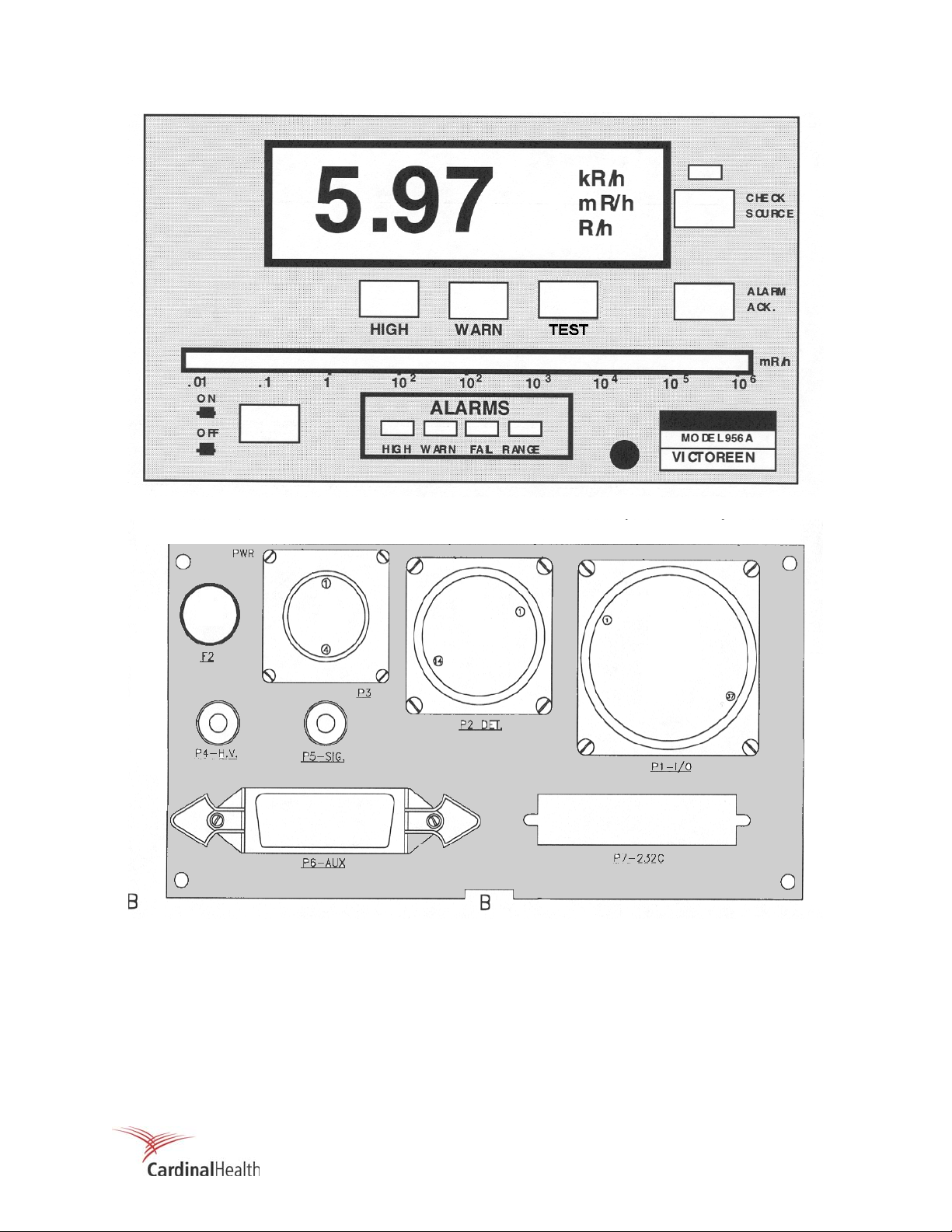
Figure 1-2. Front Panel, Model 956A-201-M2 Universal Digital Ratemeter (not to scale)
Figure 1-3. Rear Panel, Model 956A-201-M2, Universal Digital Ratemeter (not to scale)
1.11 956A-201-M2 MODIFICATIONS
Refer to Modification Sheet 956A-201-M2 for a complete description of the modification performed on this
unit.
1-11
Page 16
1.12 RECOMMENDED SPARES
Table 1-2 lists the recommended spare parts for the 955A Radiation Monitoring System.
Table 1-2. Recommended Spare Parts List
897A Detector
Part Number Description Used On
46-77 “O”-Ring, Detector Housing 897A-2X0
857-211-15 Gasket, Detector Housing 897A-2X1
857-211-19 Mounting Strap 897A-2X1
857-211-18 Detector Mounting Bracket 897A-2X1
956A-201 UDR
Part Number Description Used On
92-7027-1A Fuse F2, 2 Amp, main AC power All
19-62 Fuse F1, 50 mA, anti-jam circuit All
92-9042-A Jumper Block (10 required) All
942-200-50 Power Supply All
82-73-1 Relay All
1.13 RECEIVING INSPECTION
Upon receipt of the unit:
1. Inspect the carton(s) and contents for damage. If damage is evident, file a claim with the carrier and
notify the Cardinal Health, Radiation Management Services Customer Service Department.
Cardinal Health, Radiation Management Services
6045 Cochran Rd.
Cleveland, Ohio 44139
Phone: 440.248.9300, Fax: 440.542.3682
2. Remove the contents from the packing material.
3. Verify that all items listed on the packing list have been received and are in good condition.
If any of the listed items are missing or damaged, notify the
Cardinal Health, Radiation Management Services Customer
Service Department.
NOTE
1-12
Page 17

1.14 STORAGE
Instruments storage must comply with Level B storage requirements as outlined in ANSI N45.2.2 (1972)
Section 6.1.2(.2). The storage area shall comply with ANSI N45.2.2 (1972) Section 6.2 Storage Area,
Paragraphs 6.2.1 through 6.2.5. Housekeeping shall conform to ANSI N45.2.3 (1972).
Level B components shall be stored within a fire resistant, tear resistant, weather tight enclosure, in a
well-ventilated building or equivalent.
Instruments storage must comply with the following:
1. Inspection and examination of items in storage must be in accordance with ANSI N45.2.2 (1972)
Section 6.4.1.
2. Requirements for proper storage must be documented and written procedures or instructions must be
established.
3. In the event of fire, post-fire evaluation must be in accordance with ANSI N45.2.2 (1972), Section
6.4.3.
4. Removal of items from storage must be in accordance with ANSI N45.2.2 (1972), Sections 6.5 and
1-13
Page 18

(Blank page)
Page 19
Section 2
OPERATION
2.1 INSTALLATION
Installation consists of selecting suitable mounting sites for the detector and ratemeter, mounting the
equipment, making the required electrical connections, and entering the desired setpoints. Installation
drawings are provided in Appendix B of this manual.
Remove all power prior to installing the UDR or detector.
CAUTION
2.2 G-M DETECTOR MOUNTING
The 897A Series G-M detectors can be mounted to any suitable structure e.g. a wall or post, using the
mounting bracket (P/N 843-6-26) included with the detector. The maximum distance between the
detector and ratemeter is 2000 feet (610 meters). The detector should be mounted above normal head
height with the detector connector facing away from the area being monitored. For additional information
refer to the applicable engineering drawings, provided in Appendix B, for detector mounting dimensions.
To protect the monitor from EMI/RFI transients, the detector must be earth grounded through its wallmounting bracket.
2.3 G-M DETECTOR SETUP
The low voltage power supply input for the preamplifier is jumper selectable. This allows the use of either
a +10 Vdc or +15 Vdc supply for detector power. If the detector is used with a 956A-201 Series UDR, the
standard +15 Vdc position is used. If the detector is used in an analog radiation monitoring system, the
+10 Vdc position is used. Jumper configurations are listed in Table 2-1.
Table 2-1 Input Voltage Jumper Position
Jumper Position Input Voltage
J3 AB + 15 Vdc (factory set), digital readout
J3 BC + 10 Vdc, analog readout
The G-M tube output pulse is conditioned with a divide by 2 pulse shaping circuit to transmit a square
wave from the detector. The conditioning also permits use of the detector with analog readouts, using a
diode pump counting circuit. For use with fast rise time scalers, a jumper is provided to output the
detector pulse directly. Jumper configurations are listed in Table 2-2.
2-1
Page 20
Table 2-2 Divide Options Jumper Position
Jumper Position Divide Option
J1, J2 AB 2, square wave output (factory set)
J1, J2 BC 1, direct coupled
2.4 UDR MOUNTING
The UDR is a self-contained unit that can be mounted in four different ways.
When installing the UDR in enclosed panels or cabinets, ensure
that the maximum operating temperature (122° F) is not exceeded.
The total heat load should be calculated to determine whether
cooling by natural convection or forced ventilation (i.e. fans) is
required. The heat load for a single UDR is approximately 96
BTU/hr.
CAUTION
Where more than four units are to be mounted in a cabinet, it is
recommended that the center position in each chassis be left blank
to facilitate the flow of cooling air through the cabinet.
For seismic applications, the rear of the chassis must be
supported, or the sides of the chassis must be fastened
together. For further information, contact Cardinal Health,
Radiation Management Services.
To protect the monitor from EMI/RMI transients, the Rack
Chassis must be connected to an earth ground.
1. The first mounting utilizes a 19-inch rack chassis adapter, Victoreen Model 948-1. This configuration
requires 3.5 inches of rack height and can be used to mount up to three UDRs side by side. A blank
filler panel, Victoreen Model 948A-2, is available to cover unused mounting positions. Refer to
drawing GEL-948-1 for mounting dimensions.
Where EMI/RFI compliance is required, the Model 948B-1A-5 Dual Channel rack chassis is
available. The Model 948B-1A-5 is designed to accept two Model 956A UDR’s, mounted in the left
and right side positions. The center position is used to mount a Model S157033A2 Line Filter/Surge
Suppressor Assembly. AC power for each channel is routed to the surge suppressor, which then
feeds the AC power to the 956A UDR’s. Refer to GEL-948B-1A for mounting dimensions.
NOTE
NOTE
NOTE
2. The second mounting consists of a single channel tabletop enclosure, Victoreen Model 948-3.
Dimensions for the enclosure are 4.5 inches high by 6.8 inches wide by 14.9 inches deep. Refer to
drawing 948-3-5 for mounting dimensions.
3. The third mounting consists of a panel mount enclosure, Victoreen Model 948-9. Cutout dimensions
for this enclosure are 3.75 inches high by 6.45 inches wide; the outside dimensions for the enclosure
are 4.0 inches high by 6.7 inches wide by 13.7 inches deep. Refer to drawing 948-9-5 for mounting
dimensions.
2-2
Page 21
4. The fourth mounting utilizes the Victoreen Model 948-10 Rack Chassis Adapter to mount a 956A
UDR into an existing Victoreen analog ratemeter rack chassis such as those used for the Victoreen
842 series analog ratemeter. Refer to drawing GEL-948-10 for mounting dimensions.
The UDR is simply inserted into the selected mounting enclosure and secured using the front panel pawl
fastener.
2.5 ELECTRICAL INTERFACE
Ensure all power is off prior to connecting the field wiring
Electrical interconnections at the detector are made via the mating "MS" style connector supplied with the
detector and loop drawing S174014A-102.
Electrical interconnections to the UDR are implemented with the mating connector kit, P/N 942A-100- 4
(supplied with the readout) by using the connector input/output assignments provided in Tables 2-3
through 2-10, and loop drawing S174014A-102, provided in Appendix B. Termination instructions for
coaxial connections can be found in Appendix D. A service loop of a minimum of 12 to 16 inches should
be provided to permit partial withdrawal of the UDR for setpoint adjustment and troubleshooting.
Connector pins should be soldered to the cable using 60/40-tin/lead resin core solder and a soldering iron
of 50 watts or less.
To protect the monitor from EMI/RFI transients, the mounting chassis must be earth grounded.
Table 2-3. Rear Panel Connections
Connector Function
P1 Relay/Output, Remote Alarm Acknowledge
P2 Detector Connector
P3 AC Power Input
P4 Detector High Voltage (SHV)
P5 Detector Signal Input (BNC)
P6 Auxiliary outputs 0 – 10 Vdc & 4 – 20 mA DC
P7 RS232C, Optional
WARNING
2-3
Page 22
Table 2-4. Connector P1 – Input/Output, 956A-201-M2
Pin Signal Internal Connection
1 120 Vac Line Relay Board K1-A/V2
2 120 Vac Neutral P2-13
3 120 Vac Ground P2-11
4 Spare Relay Board K1-D
5 Spare Relay Board K1-F
6 Spare Relay Board K1-E
7 Fail Relay, Common Relay Board K3-A
8 Fail Relay, n.o. Relay Board K3-B
9 Fail Relay, n.c. Relay Board K3-C
10 Fail Relay, Common Relay Board K3-D
11 Fail Relay, n.o. Relay Board K3-F
12 Fail Relay, n.c. Relay Board K3-E
13 Warn Relay, Common Relay Board K4-A
14 Warn Relay, n.o. Relay Board K4-B
15 Warn Relay, n.c. Relay Board K4-C
16 Warn Relay, Common Relay Board K4-D
17 Warn Relay, n.o. Relay Board K4-F
18 Warn Relay, n.c. Relay Board K4-E
19 Alarm Relay, Common Relay Board K5-A
20 Alarm Relay, n.o. Relay Board K5-B
21 Alarm Relay, n.c. Relay Board K5-C
22 Spare Not Used
23 Spare Not Used
24 Spare Not Used
25 + Remote Acknowledge Main Circuit Board J9-1
26 - Remote Acknowledge Main Circuit Board J9-2
27 - 37 Spare Not Used
n.o. = normally open, n.c. = normally closed, Relays shown in shelf, or de-energized state.
Table 2-5. Connector P2 – Detector Connector, 956A-201-M2
Pin Signal Internal Connection
1 Detector + 15 Vdc Supply Power Supply + 15 Vdc
2 Not Used Power Supply – 15 Vdc
3 Supply Ground Power Supply Ground
4 + 15 V C/S On Relay K2
5 - 15 V C/S Off Relay K2
6 Not Used -
7 Not Used -
8 Not Used -
9 DC Ground Main Circuit Board J5-9
10 0 – 10 Vdc, Remote Meter Main Circuit Board J5-10
11 AC Ground P1-3 AC Ground
12 Fail, N.C (Switched, 120 Vac, Line) Relay Board K1-C (L)
13 120 Vac (Neutral) P1-2, 120 Vac (N)
14 Alarm N.C (Switched, 120 Vac, Line) Relay Board K5-E (L)
0 – 10 Vdc selected for Remote Meter use on P2 (10, 11) not P6 (5, 6).
2-4
Page 23
Table 2-6. Connector P3 – Power Input
Pin Signal Internal Connection
1 120 Vac, Line Line fuse (F2)
2 120 Vac, Neutral Power Supply, 120 Vac (n)
3 Safety Ground Chassis
Table 2-7. Connector P4 – Detector High Voltage
Pin Signal Internal Connection
MHV Detector High Voltage Direct
Table 2-8. Connector P5 – Detector Signal Input
Pin Signal Internal Connection
BNC Detector Signal Direct
Table 2-9. Connector P6 – Auxiliary I/O, 956A-201-M2
Pin Signal
1 4 – 20 mA Output #1 (+)
2 4 – 20 mA Ground (-)
3 4 – 20 mA Output #2 (+)
4 4 – 20 mA Ground (-)
5 0 – 10 V* (+)
6 Ground (-)
7 Analog Output Option (+), 0-10 mV
8 Ground (-)
9 through 24 Not used
*0 – 10 Vdc selected for Remote Meter use on P2 (10, 11) and is not available on P6 (5, 6).
Table 2-10. Connector P7 – RS232C Option
Pin Signal
1 Protective Ground
2 Transmit Data
3 Receive Data
4 Request to Send (RTS)
5 Clear to Send (CTS)
6 Data Set Ready (DSR)
7 Signal Ground
8 Receive Line Signal Detect (DCD)
20 Data Terminal Ready
Table 2-11. 897A Detector Connection
Pin Signal
K Protective Ground
H Check Source
J Check Source
E High Voltage
MTG Screw Chassis Ground
C + Voltage In
G Signal Output
2-5
Page 24

2.6 SETUP
Table 2-12 summarizes the jumper selectable configuration options. To place the system in operation,
the following steps should be performed:
Ensure you have read and fully understand Section 3 prior
to continuing.
1. Verify that jumpers and DIP switches, on the UDR and detector, are set for the operational features
desired. Refer to Section 3, Table 3-2. The 897A Detector jumpers are preset at the factory per
Tables 2-1 and 2-2, and should not be changed.
2. Apply power to the unit. The bargraph will illuminate momentarily followed with a momentary
actuation of the digital value display. The unit will then begin to display the ambient radiation at the
detector location.
The default setpoints in the UDR memory are for an 897 A-220
detector (1.00E-1 mR/h to 1.00E4 mR/h); verify the appropriate
setpoints for the actual detector are entered per Section 3
(Parameter Entry).
NOTE
NOTE
Calibration constant and detector deadtime value are obtained
from the factory calibration data sheet for each detector.
3. Detector dependent setpoints such as analog outputs, High/Low scale values, Range, Underrange,
Overrange limit, calibration constant, and detector deadtime may now be verified and if required,
modified using the procedures outlined in Section 3.
4. Channel dependent setpoints such as alarm limits may be verified, and if required, modified using the
procedures outlined in Section 3.
5. Electronic adjustments affecting calibration are factory set and should not be readjusted for initial
operation unless the UDR has been in storage for more than one year. If the Unit has been in
storage for more than one year, the electronic calibration described in Section 4 should be performed.
NOTE
2-6
Page 25

Table 2-12. Model 956A-201-M2 Option Jumpers
Jumper Function Position Operation
JP1 Microprocessor Reset Out
In
JP2 PROM Type 1-2
2-3
JP3-1/JP3-2 Statistical Accuracy (Note: This
accuracy refers only to the
statistical interpretation of
detector counts, and not
Out/Out
Out/In
In/Out
In/In
Normal Operation (factory) Momentary
connect to reset microprocessor without
cycling AC power
Not Applicable
PROM 27128
PROM 27256 (factory)
2% Accuracy – Not Implemented
5% Accuracy – Not Implemented
10% Accuracy – Not Implemented
Fixed one second display update (factory
detector accuracy)
JP3-3 Alarm Acknowledge In
Out
JP3-4 Fail Alarm In
Out
JP3-5 Check Source Alarm In
Out
JP4 Shield Polarity Selection 1-2
2-3
Manual Acknowledge (factory)
Automatic
Enable No Counts Fail Alarm (factory)
Inhibit No Counts Fail Alarm
Alarm Inhibited (factory)
Alarm Enabled
Negative Input Pulse (Other Detectors)
Positive Input Pulse (G-M Detectors)
(factory)
JP5 Shield Polarity Selection 1-2
2-3
JP-6 Anti-Jam Fuse Selection 1-2
2-3
JP7 Detector Type for Anti-Jam
Circuit Timing
1-2
2-3
Out
Shield for Negative Pulse
Shield for Positive Pulse (G-M) (factory)
Enable for Normal Operation (factory)
Anti-Jam Circuit fuse bypassed (testing)
Scintillation
G-M Tube (factory)
Anti-Jam Circuit Disabled (for testing only)
2-7
Page 26

(Blank page)
Page 27

Section 3
THEORY OF
OPERATION
3.1 OPERATION
This section describes the operation and set up of a Digital Area Monitoring System. The system consists
of a Model 956A-201-M2 UDR and a Model 897A Series G-M Detector. The detector preamplifier
provides the electronics interface between the detector and the UDR. The preamplifier provides input
pulse discrimination, pre-divide capability, anti-jam circuitry, pulse amplification and output drive
capabilities. The output of the preamplifier is transmitted to the UDR. The 956A-201-M2 UDR uses this
information to generate the dose rate display, error codes, alarms, and analog outputs.
Operation of the 956A-201-M2 UDR consists of operator functions and configuration functions. All
operator functions are performed using the front panel shown in Figure 1-2. Configuration functions are
performed using internal switches and/or jumpers, which are accessible with partial removal of the UDR
from the mounting enclosure. Calibration involving trim pots is described in Section 4.
For applications where EMI/RFI compliance is required, the S157033A2 Line Filter/Surge Suppressor
Assembly, designed to provide EMI/RFI protection for the 956A Series digital ratemeter and 897A Series
G-M detectors, is available. The assembly consists of two (2) separate and independent line conditioning
circuits that provide filtered AC power to each 956A Series ratemeter. The S157033A2 is designed to
mount in the center section of the 948B-1A-5 dual module rack chassis, to provide EMI/RFI protection for
two (2) 956A Series ratemeters.
3.2 DETECTOR OPERATION, MODEL 897A-2XX
The Digital Area Monitor uses a Model 897A-2XX G-M tube as a gamma radiation detector. The tube is
filled with a mixture of gases, one of which acts as a quenching agent, while the others tend to support
ionization. Electrically, it consists of a positive electrode (anode), which is maintained at a steady potential
of 500/650 Vdc and a negative electrode (cathode) that is near ground potential.
When a gamma photon penetrates the shield encasing the G-M tube, an ionizing event occurs. An ion
pair is produced, triggering an avalanche of ion pairs. The current pulses produced (one pulse per ionizing
event) are independent of the energy of the initiating particle. Multiple discharge, caused by the release of
electrons from the cathode due to excess energy, is eliminated after a short time (called dead time,
typically 20-45 microseconds) by a quenching gas within the tube. The resulting pulses are conditioned
and transmitted to the preamplifier.
The integral detector preamplifier provides input pulse discrimination and amplifies pulses received from
the G-M tube to 5 Vdc amplitude. The current drive output of the preamplifier will drive a signal up to 2000
feet through a 50-ohm transmission line, without signal degradation.
3-1
Page 28

Should a very high intensity radioactive source be detected, the G-M tube may become saturated (i.e.
pulses are separated by a period less than the dead time of the tube). This would have the effect of
holding the preamplifier output at a relatively constant output voltage, resulting in count loss at the readout.
Anti-Jam circuitry in the preamplifier produces a full-scale output square wave signal, providing a full-scale
indication at the readout.
G-M Detector Response Time
The response time of the system to a step change in radiation value is 60 seconds, due to the operation of
the pulse counting algorithms. The detector radiation value displayed is the result of a rolling average of
the latest 60, one-second values, and is updated once per second. An alarm will be initiated within one
second after the current one-minute average exceeds the alarm setpoint.
Check Source
A manual check source may be initiated from the UDR by the operator to check detector operation. The
Check Source push-button is a momentary contact switch, and is active as long as the pushbutton is
depressed. Upon initiation and removal of the check source request, the internal counting registers are
cleared and the display value will be based on the number of new values received. After 60 seconds, the
display value will reflect the average of the past 60 values. During check source activation, analog outputs
are muted (forced to zero). The High and Warn alarms are normally inhibited during check source
operation, but may be enabled by removing Jumper JP3-5, on the UDR main printed circuit board (see
Table 2-12). The counters are cleared upon exiting Check Source mode, resulting in a display of 0.00.
After one minute, the current radiation value will be displayed.
3.3 UDR OPERATION, MODEL 956A-201-M2
Operation of the 956A-201-M2 UDR consists of operator functions and configuration functions. All
operator functions are performed using the front panel. Configuration functions are performed using
internal switches and/or jumpers that are accessible via partial removal of the UDR from the mounting
enclosure.
Normal Operation
If the measured radiation field is within the range of the detector during power-up, the mR/h value will be
displayed as a three digit number: N.NN, where N = 0 to 9. A backlit insert will display engineering units in
mR/h, R/h, or kR/h. The bargraph will display the value on the fixed mR/h scale and any indicator lights
that are on should be green, providing the operator with a visual indication of normal operation. The
analog outputs will track the displayed value, and the alarm outputs will be active. The Warn, High, and
Fail relays operate in the Fail Safe Mode.
WARN/HIGH Alarms
If the measured radiation field increases above the WARN alarm limit, the WARN alarm indicator will turn
on flashing (amber color), the bargraph will change color to amber, and the warn alarm relay will deactivate. If the measured radiation field increases above the HIGH alarm limit, the HIGH alarm indicator
will turn on flashing (red color), the bargraph will change color to red, and the high alarm relay will deactivate.
Non-fail-safe relay operation for the HIGH and WARN alarms is
available as a firmware option at time of purchase.
NOTE
3-2
Page 29
The UDR can be configured to automatically reset the alarm relays and alarm indicators, or it can hold the
alarm relays de-energized and flash the alarm indicators until the alarm acknowledge (ALARM ACK)
pushbutton is pressed. If the ALARM ACK pushbutton is pressed while the alarm condition still exists, the
indicators will go to a steady state, and the relays will remain de-energized until the alarm condition returns
to normal. Upon resumption of normal operation, the relays will energize and alarm indicators will
extinguish. The bargraph color will always indicate the current status; green for normal, amber for warn,
and red for a high alarm.
Front panel pushbuttons labeled HIGH and WARN can be used to display the respective alarm set points.
To drive a local alarm, a 120 Vac is internally wired from alarm output connector P1 to the alarm relay
contact on P2-13 and 14. Refer to Modification Sheet 956A-201-M2MS and Loop Drawing S174014C-
102.
Range Alarm
If the measured radiation field is below the underrange setpoint (minimum range of the detector used), the
front panel display will indicate 0.00 mR/h, the bargraph will indicate the actual radiation value, and the
RANGE alarm indicator will illuminate in red. The minimum range is adjustable by the underrange
setpoint, and is defaulted to 1.00E-1 mR/h. When the measured radiation field increases into the range of
the detector, the RANGE alarm indicator will extinguish and normal operation will begin.
There are three ranges for the ratemeter, one for each detector range (low, medium, & high). The specific
range for each detector is established by operator-entered setpoints (refer to "Setpoint Entry" for actual
entry procedures). The detector range for each specific detector is shown below.
Detector
897A-210/211 0.01 to 10E3 mR/h 1.00E-2 1.00E3
897A-220/221 0.1 to 10E4 mR/h 1.00E-1 1.00E4
897A-230/231 1 to 10E5 mR/h 1.00E0 1.00E5
If the measured radiation field goes above the overrange setpoint, the RANGE alarm indicator will
illuminate and the front panel display will indicate EEEEE, the bargraph will illuminate in red, and the
analog output will be set to full scale. The maximum range of the detector used is determined by the
overrange setpoint. When the measured radiation field returns within the maximum operating range of the
detector and the condition is acknowledged, the RANGE alarm indicator will extinguish and normal
operation will resume.
In addition to the display of EEEEE when in Overrange, the
In the event the detector output exceeds the electronic anti-jam circuit trip level, the anti-jam fuse will open
and the Fail relay will change state to indicate a monitor not in service condition. Replacement of the antijam fuse (F1) will be required in order to return the rate meter to normal operation.
Detector Range
Underrange Setpoint Overrange Setpoint
NOTE
mR/h engineering units will be displayed if the HIGH or WARN
front panel set point display pushbuttons have been accessed.
IF desired, the mR/h units display may be cleared by either
pressing the ENTER push button, or cycling the UDR power
OFF/ON. The mR/h unit’s display, however, does not affect the
operation of the Overrange function.
FAIL Alarm
Detector failure, detector overrange, or microprocessor failure are some of the conditions which can
produce a FAIL alarm and in some cases an error display. The Fail condition is true whenever any
equipment failure is detected and false when no equipment failures are detected.
3-3
Page 30

When a Fail condition occurs, other than power failure, the red FAIL alarm indicator illuminates and the
Fail relay coil de-energizes. On the 956A-201-M2, auxiliary relay K1 is hard wired to operate in parallel
with the Fail relay, to drive a local indicator. Internally, 120 Vac is hard wired from alarm output connector
P1 to the Fail relay contacts on P2-12, and 13. Refer to Modification Sheet 956A-201-M2MS and Loop
Drawing S174014C-102.
To return the channel to normal operation after a FAIL alarm, the condition that caused the alarm must be
located and corrected. Upon correction of the failure condition, the FAIL alarm will automatically close.
Check Source
The check source pushbutton and electronics are provided to verify detector operation. To operate the
check source, press the CHECK SOURCE pushbutton and hold it down. The Check Source LED will
illuminate, and the radiation value will increase. Releasing the check source pushbutton will allow normal
UDR operation. An internal configuration jumper (JP3-5) allows alarms to be activated or deactivated in
the check source mode. The analog outputs are forced to their low scale value during a check source
operation.
Trip Test, 956A-201-M2
A Trip Test Function has been added to the operating firmware of the 956A-201-M2. The purpose of the
function is to verify operation of the output relay, status indicators, display, and analog outputs.
Refer to the Operational Mode section for a complete description of Operation.
Firmware Version
This system requires a PROM for UDR operation. For the part number and the latest revision of the
PROM, see the Factory Test Data Sheet. Operation as described in this manual pertains to the PROM
defined in Section 1.1.
3.4 OPERATIONAL MODES
Normal Operation, Mode
The UDR is in normal operation when the UDR function switch is in any position except 8, and the Check
Source button is OFF. During normal operation, the display shows the dose rate data received from the
preamplifier in mR/h, R/h, or kR/h. The bargraph will also show the dose rate. The color of the illuminated
segments is green when the dose rate is below the WARN setpoint, amber when the dose rate is above
the WARN setpoint and below the HIGH setpoint, and red when the dose rate is above the HIGH setpoint.
The analog outputs are active and all alarms are enabled.
Data Entry Mode
Data Entry Mode is selected by pressing the ENTER pushbutton while the rotary FUNCTION switch is in a
valid setpoint position (see Setpoint Description). The selected setpoint is displayed in exponential
format (e.g. 1.00E2) with the left most digit flashing. Setpoints are entered in exponential format (e.g.
X.XXEN), where X is the mantissa and N is the exponent. The X value may be any integer value between
0 and 9. A positive exponent is entered by selecting the "E" symbol, and a negative exponent is entered
by selecting the "-" symbol. The N value may be any integer value between 0 and 9. If the FUNCTION
switch is not in a setpoint position, pressing the ENTER button has no effect. Refer to Table 3-3 for
FUNCTION switch positions.
In the Data Entry Mode, the bargraph and analog outputs remain active.
3-4
Page 31

Alarm Inhibit Mode
Alarms are inhibited in situations where an alarm trip would be meaningless because the UDR is not in a
normal measurement mode (i.e., when the UDR is in the Check Source Mode). New alarm trips cannot
occur and old alarms cannot be reset. When the inhibit period is over, alarm trips and resets are enabled
again. Alarm inhibit conditions are discussed in the following paragraphs.
3-5
Page 32

Check Source Mode
The check source pushbutton and electronics are provided to verify detector operation. To operate the
check source, press the CHECK SOURCE pushbutton and hold it down. The check source relay will
energize, the check source indicator will illuminate (green), and the check source mechanism will expose
the check source (sealed capsule of
detector printed circuit board. The counters will be cleared and radiation values displayed on the front
panel will reflect the average of the new values received. Releasing the check source pushbutton will
return the source capsule to its shielded position, clear the radiation value stored in the UDR counter and
extinguish the check source indicator, allowing normal UDR operation to resume. After approximately 60
seconds, the displayed value will indicate the average of the previous 60 one-second values stored. An
internal configuration jumper (JP3-5) allows alarms to be activated or muted if alarm limits are exceeded
by the check source radiation value.
The bargraph operates normally during Check Source operation.
The bargraph and alarms are inhibited from changing state for five (5) seconds upon entry and exit of the
Check Source function.
The front panel Alarm and Warn status indicators are disabled during Check Source operation.
The analog outputs are set to zero (i.e. 4 mA or 0V) during Check Source operation.
36
CI) to the G-M tube by positioning the source over an access on the
Calibration (scaler) Mode Operation
Calibrate mode for the UDR is entered by turning the rotary setpoint switch to position 8 and pressing the
ENTER button.
The current calibration time setpoint is displayed in seconds, with the first digit flashing to indicate the edit
mode. The bargraph will turn off, the analog output will remain fixed at their value just prior to entering
Calibrate, the Fail LED will illuminate, the radiation unit backlights will turn off, the HIGH, WARN and
Range LED’s will turn off, and the Fail Safe High, WARN and Fail relays will de-energize. The calibration
setpoint may be edited, but will reset to 60 seconds whenever the unit is turned off or the functional switch
is moved from position 8.
Once the desired calibration time is set, momentarily pressing the ENTER button again will start the
calibration. The display will go to zero and the unit’s backlight will begin to flash. The UDR will count for
the entered calibration time, displaying the current summation of counts each second. When the
calibration is completed, the final summation of counts for the calibration time is displayed and the unit’s
backlights will be steady on.
Another calibration can then be executed by pressing the ENTER key, and the system will again display
the calibration time for editing. Pressing the Enter button again will start the Calibrate timer. A calibration
in process can be stopped by pressing the ENTER key or by moving the rotary switch to a position other
than position 8. The calibration mode is exited by moving the rotary function switch out of position 8. The
UDR will reset, the Fail Safe High, Warn, and Fail relays will energize, and the UDR will continue normal
operation.
When the calibrate mode is initiated (i.e. rotary setpoint switch at
position 8 and the Enter button is pressed), the Alarm, Warn, and
Fail relays change state to indicate the monitor is in a nonoperational state.
NOTE
3-6
Page 33

The calibration mode can also be entered with the UDR in the check source mode of operation. Move the
rotary switch to position 8 and press the check source button. While holding down the check source
button, press the ENTER button. This will turn the Check Source LED on, actuate the check source relay,
and lock the Check Source function on. The Check Source button may now be released and the Check
Source will remain on. Pressing the enter button again will start the calibration. The check source light
will remain on, indicating that the check source relay is energized. The check source condition will clear
when the calibrate mode is exited.
In Calibrate mode, the analog outputs are frozen at their last value, prior to entering the Calibrate mode.
In Calibrate mode, any High and Warn alarms are cleared, the Fail LED is turned on, and the Fail Safe
Alarm, Warn and Fail relays change state, to indicate the unit is not monitoring radiation.
In Calibrate mode, the bargraph display is blanked.
Trip Test Mode, 956A-201-M2
The Trip Test Mode is provided to verify operation of the output relays, status indicators, display and
analog outputs. The Trip Test Mode is entered by pressing and holding in the front panel TEST
pushbutton. The Trip Test Mode is exited by releasing the TEST pushbutton, and then pressing and
releasing the ACKNOWLEDGE pushbutton.
Pressing the TEST pushbutton will cause the Alarm, Warn and Fail
relays to change state and indicate an alarm condition. Prior to
activating the Test Mode ensure the appropriate plant personnel
are notified.
NOTE
A detailed description of the operation is as follows:
TRIP TEST pushbutton depressed to initiate Trip Test Mode
• Front panel display shows 8.8.8.8.8
• KR/h, mR/h and R/h Backlights are illuminated
• Bargraph is fully illuminated, in amber
• HIGH Alarm relay changes state (de-energize)
• WARN Alarm relay changes state (de-energize)
• Aux Relay changes state (de-energize)
• Fail relay changes state (de-energize)
• High, Warn, Fail. Range, and Check Source LEDs are illuminated
• Analog Outputs are at Full Scale
TEST pushbutton Released
• Front panel display shows current value and continues to count
• mR/h backlight is illuminated
• Bargraph will display the actual count rate in Red
3-7
Page 34

If the count rate is below the range limit of the paragraph, the
bargraph will be blanked. When an input signal is present, the
bargraph will illuminate in red as a result to the unacknowledged
alarm condition resulting from actuating the Test Function.
• HIGH Alarm relay changes state (energize)
• WARN Alarm relay changes state (energize)
• Aux Relay changes state (energize)
• Fail relay changes state (energize)
• High and Warn LEDs are illuminated, flashing
The Trip Test Function takes precedence over the automatic alarm
reset option, and the ACK pushbutton, in the next step, must be
pressed to clear the alarm LED’s and bargraph.
• Fail, Range, and Check Source LEDs are turned off and return to normal
• Analog Outputs return to normal
Press and release the ACK pushbutton
NOTE
NOTE
• No Change, display shows current value
• No Change, mR/h backlight is illuminated
• Bargraph will return to normal, displaying actual count rate
• No Change, HIGH Alarm relay
• No Change, WARN Alarm relay
• No Change, Aux Relay
• No Change, Fail relay
• High and Warn LEDs are off, and return to normal operation
• No Change, Fail, Range, and Check Source LEDs return to normal
• No Change, Analog Outputs return to normal
3.5 ALARMS
The alarm functions provided by the UDR include HIGH, WARN, FAIL, and RANGE. The HIGH, WARN,
and FAIL alarms drive relay contact outputs. Some operating modes of the UDR disable alarms. The user
is cautioned to read and fully understand section 3.
Alarm Logic Types
Alarm logic defines whether the alarm is reset manually or automatically and whether alarm relay coils are
energized or de-energized in normal operation.
Standard alarm reset logic for the UDR is manual reset for the HIGH and WARN alarms, and auto reset for
the RANGE and FAIL alarm. Fail-safe operation is also standard.
3-8
Page 35

Auto reset for the HIGH and WARN alarms may be selected by jumper JP3-3.
Manual Reset
When an alarm trips, the relay coil goes to its abnormal position. The indicator flashes until the alarm is
acknowledged by pressing the ALARM ACK button on the UDR. The indicator then remains steady on
until the alarm condition becomes false. At that time, the alarm resets by turning the indicator off and
returning the contact to its normal position.
Auto Reset
When an alarm trips, the contact goes to its abnormal position. The indicator goes steady on. When the
alarm condition becomes false, the alarm automatically resets, returns the relay coil to normal position,
and turns the indicator off.
Auto reset may be selected for the HIGH and WARN alarms by removing jumper JP3-3 from the UDR
main board.
Standard relay operation for the UDR is fail-safe. When the unit is powered, the relay coil energizes. If
power is lost to the relay coil, or an alarm condition occurs, the relay de-energizes, giving a trip indication.
This logic provides fail-safe operation for the alarm function.
Non-Fail-safe relay operation for the HIGH and WARN alarms is available as an option.
High Alarm
The HIGH alarm condition is “true” when the display dose rate is greater than or equal to the HIGH alarm
setpoint and “false” for all other conditions.
The standard logic for the HIGH alarm is fail-safe, manual reset.
When the HIGH alarm is tripped, the red HIGH alarm indicator begins flashing, the bargraph goes to red,
and the HIGH alarm relay coil de-energizes. When the alarm is acknowledged, the HIGH alarm indicator
goes steady on.
The HIGH alarm relay will change state (i.e. energize) after the Acknowledge push button is pressed and
the radiation value drops below the setpoint.
The HIGH alarm is normally inhibited in Check Source mode. By removing jumper PJ3-5, the HIGH and
WARN alarms may be enabled in check Source mode.
The firmware will not accept a High setpoint that is lower than the Warn set point. On the 956A-201-M2,
Error Code E0004 will be displayed.
On the 956A-201-M2, 120 Vac is wired to high alarm relay
contacts P2-13 and 14.
NOTE
WARN Alarm
The WARN alarm condition is “true” when the display dose rate is greater than or equal to the WARN
alarm setpoint and “false” for all other conditions.
The standard logic for the WARN alarm is fail-safe, manual reset.
When the WARN alarm is tripped, the amber WARN alarm indicator begins flashing, the bargraph goes to
amber, the WARN alarm relay coil de-energizes. When the alarm is acknowledged, the WARN alarm
indicator goes steady on. With the alarm acknowledged, the relay will change state when the radiation
value drops below the setpoint.
3-9
Page 36

The WARN alarm is normally inhibited in Check Source mode. By removing jumper JP3-5, the HIGH and
WARN alarms may be enabled in Check Source mode.
The firmware will not accept a Warn setpoint that is higher than the High setpoint. ON the 956A-201-M2
Error Code E0004 will be displayed.
RANGE Alarms
The underrange condition is "true" when the dose rate is below the underrange setpoint and "false" for all
other conditions. The RANGE indicator illuminates, the analog output is set to zero, and the display reads
0.00 mR/h when the underrange condition is true. The bargraph will operate normally. The Alarm, Warn,
and Fail relays are not affected by the underrange alarm.
The underrange condition clears automatically when the detector output returns within the normal range.
There is no relay associated with the UNDERRANGE alarm.
The OVERRANGE is true when the dose rate is greater than or equal to the overrange setpoint or the
Model 897A preamplifier is sending an output pulse greater than the detector preamplifier Anti-Jam circuit
setpoint. The condition is false when neither of the conditions are true.
When the OVERRANGE alarm is active, WARN and HIGH alarms are true, the red RANGE indicator
illuminates, the bargraph illuminates red, the analog output reads full scale, and the display reads EEEEE.
The OVERRANGE alarm setpoint is operator adjustable.
NOTE
In addition to the display of EEEEE when in Overrange, the
mR/h engineering units will be displayed if the HIGH or WARN
front panel set point display pushbuttons have been accessed.
IF desired, the mR/h units display may be cleared by either
pressing the ENTER push button, or cycling the UDR power
OFF/ON. The mR/h unit’s display, however, does not affect the
operation of the Overrange function.
The OVERRANGE alarm must be reset by pressing the acknowledge pushbutton when the overrange
condition is false (i.e. radiation level returns to a value below the overrange setpoint). The OVERRANGE
alarm will not reset automatically, at a later time, after the acknowledge pushbutton is pressed as it does
for the HIGH and WARN alarms. If auto reset is selected for HIGH and WARN alarms, these will reset
automatically, but the overrange display will remain until the acknowledge pushbutton is pressed.
In addition, if the detector output is above the electronic anti-jam circuit threshold of the UDR, the anti-jam
circuit will be activated, opening the anti- jam fuse on the UDR. This causes the Fail LED to turn on, the
Fail relay to change state, and the detector High Voltage power supply to turn off indicating a nonoperational mode. After the anti-jam condition has cleared, to return to normal operation, the 956A UDR
must be powered off, the anti-jam fuse replaced, and the power turned back on.
FAIL Alarms
Several equipment failure conditions are monitored which produce a FAIL alarm and in some cases an
error message. The Fail condition is "true" whenever any equipment failure is detected and "false" when
no equipment failures are detected. When a Fail condition occurs, other than power failure, the red FAIL
alarm indicator illuminates and the Fail relay coil de-energizes.
The FAIL alarm logic is always fail-safe, auto reset.
3-10
Page 37

The following are the FAIL alarms included in the 956A-201-M2 UDR:
1. NO COUNT Failure
2. POWER Failure
3. MPU Failure (hardware)
4. Anti-Jam Trip
No Count Failure
If no pulses are received by the UDR for five minutes, a no count failure is detected. A no count alarm
usually indicates a failure in the detector or UDR detector high voltage supply. The UDR display, however,
may read zero for five minutes or more without a low signal FAIL alarm. This is because the re-amplifier is
reporting a non-zero dose rate that is below the low range value. The No Count failure alarm can be
disabled by removing jumper JP3-4 from the UDR main board.
Power Failure
If power is lost to the UDR, the bargraph, alarm indicators, and the display are blanked (turned off). The
HIGH, WARN, and Fail relay coils de-energize.
MPU Failure
If the Fail timer circuit, which checks the MPU (main processor) function, is allowed to time out (because of
a hardware failure), a failure condition will be indicated.
In the unlikely event of a watchdog timer trip, the display may
“Freeze” or the unit may appear to be operating normally. The
Fail Alarm, however, will remain de-energized until a refresh
signal is provided from the microprocessor to prevent the Fail
Timer from timing out. It is to advise the operator of this condition,
recommended that the Fail Relay contact be wired into the user’s
radiation monitor trouble anunciator.
NOTE
Anti-Jam Trip
Should the detector output exceed the UDR anti-jam circuit threshold, the anti-jam fuse opens the detector
high voltage is shut down the Fail LED will illuminate, and the Fail relay will de-energize.
ON the 956A-201-M2, 120 Vac is wired to Fail relay contacts P212 and 13. Auxiliary relay K1 is internally wired to operate in
parallel with the Fail relay.
NOTE
3.6 JUMPER SELECTABLE CONFIGURATION FUNCTIONS
The UDR contains a series of eleven hardware jumpers and nine user specified setpoints that affect
operation of the unit.
The jumpers are designated as JP1 and JP2, JP3-1 through JP3-5, and JP4 through JP7. Refer to the
main circuit board assembly drawing located in Appendix B of this manual for jumper locations. The
functions affected by JP1 through JP7 are described in the following paragraphs and shown in Table 3-2.
3-11
Page 38

The unit will only read jumper selection on power-up; therefore,
the unit must be turned off when changing jumpers.
NOTE
Microprocessor Reset
Jumper JP1 permits local reset of the microprocessor without cycling AC power.
PROM Type
Jumper JP2 must be installed in position 2-3 for use with the 27256 PROM installed.
Count Time Selection (Statistical Accuracy)
The statistical accuracy jumpers JP3-1 & JP3-2, are not implemented. This statistical accuracy, count
time and consequently, the update time of the display are fixed. The unit is shipped from the factory with
both JP3-1 and JP3-2 installed, resulting in a displayed value that is the sum of 60, one second values,
updated once per second.
Alarm Reset (Acknowledge)
1. JP3-3 OUT - The unit resets alarm indicators and alarm relays after the radiation value falls below the
setpoint without regard to the alarm acknowledge pushbutton.
2. JP3-3 IN - The unit maintains the alarm indicators and alarm relays in the alarm state until the alarm
acknowledge pushbutton has been pressed and the radiation value falls below the setpoint. If the
alarm acknowledge pushbutton is pressed while the radiation value is still above the setpoint, the
flashing indicator will go to a steady state ON condition.
The UDR is normally shipped from the factory with JP3-3 installed.
No Counts FAIL Alarm
JP3-4 IN - The unit will go into a FAIL mode after five minutes with no counts from the detector.
JP3-4 OUT - The unit will not go into a FAIL mode when there are no counts from the detector.
The UDR is normally shipped from the factory with JP3-4 installed.
Inhibit Alarms (Check Source Operation)
1. P3-5 OUT - The alarms will become active during check source operation if alarm limits are exceeded.
2. JP3-5 IN - Alarms are inhibited during check source operation, but if the unit is in an alarm condition
when the check source is activated, it will remain in the alarm condition.
The UDR is normally shipped from the factory with JP3-5 in.
Input Pulse Selection
Jumper JP4 is set to position 2-3 for G-M detector inputs. Position 1-2 is provided for use with other
detectors.
Input Shield Polarity
Jumper JP5 is set to position 2-3 for G-M detector inputs. Position 1-2 is provided for use with other
detectors.
3-12
Page 39

Anti-Jam Selection
Jumper JP6 is normally installed in position 1-2. Position 2-3 bypasses the anti-jam fuse for test purposes.
Detector Type
Jumper JP7 is set to position 2-3 for a G-M detector input. Position 1-2 is provided for use with a
scintillation detector. Removing the Jumper disables the anti-jam circuit for test purposes.
Table 3-2. Model 956A-201-M2 Option Jumpers
Jumper Function Position Operation
JP1 Microprocessor Reset Out
IN
JP2 PROM Type 1-2
2-3
JP3-1/JP3-2 Statistical Accuracy (Note: this
accuracy refers only to the
statistical interpretation of
detector counts, and not
detector accuracy)
JP3-3 Alarm Acknowledge In
JP3-4 Fail Alarm In
JP3-5 Check Source Alarm In
JP4 Input Pulse Selection 1-2
JP5 Shield Polarity Selection 1-2
JP-6 Anti-Jam Fuse Selection 1-2
JP7 Detector Type for Anti-Jam
Circuit Timing
Out/Out
Out/In
In/Out
In/IN
Out
Out
Out
2-3
2-3
2-3
1-2
2-3
Out
Normal Operation (factory) Momentary connect to
reset microprocessor without cycling AC power
Not Applicable
PROM 27128
PROM 27256 (factory)
2% Accuracy – 9604 Target Counts, Not
implemented
5% Accuracy – 1537 Target Counts, Not
implemented
10% Accuracy – 384 Target Counts, Not
implemented
Fixed one second display update of 60 one
second values (factory)
Manual Acknowledge (factory)
Automatic
Enable No Counts Fail Alarm (factory)
Inhibit No Counts Fail Alarm
Alarm Inhibited (factory)
Alarm Enabled
Negative Input Pulse (Other Detectors)
Positive Input Pulse (G-M Detectors) (factory)
Shield for Negative Pulse
Shield for Positive Pulse (G-M) (factory)
Enable for Normal Operation (factory)
Anti-Jam Circuit fuse bypassed (testing)
Scintillation
G-M Tube (factory)
Anti-Jam Circuit Disabled (for testing only)
3.7 POWER UP PROCEDURE
To place the system in operation, the following steps should be performed:
1. Verify that the UDR configuration jumpers are properly selected. Refer to Section 3.6 "Configuration
Functions" for addition information if required.
2. Verify that the UDR Function switch, located on the front right section of the UDR main board, is in a
position other than 8.
3. Verify that the detector and UDR are properly connected.
4. Apply power to the system. If all connections are good, the UDR will power up and will begin to
monitor the ambient radiation level.
3-13
Page 40

The appearance of error codes E0002 or E0008 may indicate that
the setpoint memory has not been initialized. To initialize the
setpoint memory to the default values, power-up the UDR with
the ENTER button held down. (The UDR must be pulled out from
its mounting to access the ENTER button).
5. Detector dependent setpoints (i.e. analog output High/Low scale values, range, underrange,
overrange, calibration constant, detector deadtime) and channel dependent setpoints, (i.e. as alarm
limits), may be entered using the procedure described in this section. The UDR contains default
values for all setpoints to permit power-up prior to user-defined values being entered.
Ensure the setpoints entered are within the normal range of
expected operation before entry, or spurious alarms may be
generated.
6. Electronic adjustments affecting calibration are factory set and should not be readjusted for initial
operation unless the UDR has been in storage for more than one year. If the unit has been in storage
for more than one year, the electronic calibration described in Section 4 should be performed.
NOTE
NOTE
3.8 UDR FUNCTION SWITCH AND PARAMETER ENTRY
Table 3-3 shows the UDR Function Switch positions and the function.
Table 3-3. UDR Function Switch Positions/Function
Switch Position Function
0 Selects HIGH Alarm Setpoint
1 Selects WARN Alarm Setpoint
2 Selects Resolving Time (Detector Dead Time)
3 Selects Analog Full Scale Limit
4 Selects Overrange Limit
5 Selects Conversion Constant
6 (Not Used)
7 Selects Analog Low Scale
8 Selects Calibrate Mode
9 Selects Underrange Value
Parameter Entry
Parameter entry is accomplished using a sixteen position rotary switch labeled FUNCTION and three
momentary pushbutton switches labeled ENTER, VALUE, and DIGIT. These switches are located on the
right side of the main circuit board about two inches behind the front panel and are accessible by partially
removing the unit from its mounting case.
The FUNCTION switch is used to select the parameter to be entered. It is located on the right side of the
main board, directly in front of the power supply. Table 3-4 defines the switch positions and a description
of each parameter can be found in the following paragraphs.
3-14
Page 41

Table 3-4. Function Switch Entry Parameters
Switch
Position
0 High Alarm Limit mR/h ** ** ** 1.00E3
1 Warn Alarm Limit mR/h ** ** ** 1.00E1
2 Resolving Time
3 Analog Full Scale
4 Overrange Limit mR/h 1.00E3 1.00E4 1.00E5 1.00E4
5 Conversion
6 Not Used N/A E0007 E0007 E0007 E0007
7 Analog Low Scale
8 Calibration
9 Underrange Limit mR/h 1.00E-2 1.00E-1 1.00E0 1.00E-1
A through F Not Used - E0007 E0007 E0007 E0007
* Detector unique, provided with the detector/detector calibration sheet.
** User Selected (detector range dependent).
To enter or display a parameter, the FUNCTION switch is set to the desired position and the following
steps are performed:
Setpoint Units Detector
897A-21X
minutes * * * 0.00E0
(Dead Time)
mR/h 1.00E3 1.00E4 1.00E5 1.00E4
Value
mRh/CPM * * * 1.00E-2
Constant
mR/h 1.00E-2 1.00E-1 1.00E0 1.00E-1
Value
seconds ** ** ** 6.00E1
Mode/Time
Detector
897A-22X
Detector
897A-23X
Default
Value
In the event it is necessary to re-enter all of the default setpoints,
the UDR EPROM memory may be reinitialized by turning the
UDR power off, then depressing the ENTER pushbutton at the
same time the power on switch is depressed. Releasing the
ENTER pushbutton and momentarily depressing the ENTER
pushbutton again to exit the setpoint entry mode and return to
normal operation.
1. Press the ENTER pushbutton. The current value of the parameter, selected by the FUNCTION switch
will be displayed on the front panel. The leftmost digit of the value will be flashing. The value is
displayed in the format shown below.
M.MMEN
This format expresses the form of M.MMEN, where M is a whole number from 0 to 9, E designates a
positive exponent, and N represents the exponent value from 0 to 9. A negative exponent is
expressed as a minus (-) character in the E position. Pressing the Enter button again enters the
value currently displayed into non-volatile setpoint memory.
2. The value of the flashing digit can be incremented by pressing the VALUE pushbutton.
3. The flashing digit can be moved one place to the right by pressing the DIGIT pushbutton.
4. When the desired value has been entered into the display, pressing the ENTER pushbutton causes
the displayed value to be entered into non-volatile memory for permanent storage. The new
parameter value is now effective.
NOTE
3-15
Page 42

5. Refer to Table 3-4 for a listing of function switch setpoint descriptions.
6. The firmware in the UDR checks alarm, and analog range setpoints for invalid conditions, and will not
accept an invalid setpoint (i.e. Warn alarm greater than High alarm, High alarm less than Warn alarm)
as defined in Setpoint Descriptions, Section 3.8. After a setpoint has been changed, the operator
must re-display the setpoint, to verify the new setpoint has been accepted.
7. During setpoint entry, the bar graph and analog outputs function normally. Once the setpoint is
entered, the impact of the changed value, if any, will be seen.
3.9 SETPOINT DESCRIPTIONS
High Alarm Limit, Setpoint 0
This setpoint is entered in units of mR/h in the exponential format X.XXEN. The high alarm limit setpoint
can be set to any value desired. When the display value exceeds this limit, the UDR will go into a HIGH
alarm state. The HIGH alarm limit must be greater than or equal to the WARN alarm and the underrange
limit. It must be less than or equal to the overrange limit.
Warn Alarm Limit, Setpoint 1
This setpoint is entered in units of mR/h in the exponential format X.XXEN. The warn alarm limit setpoint
can be set to any value desired, but must be lower than the high alarm limit setpoint. When the displayed
value exceeds this limit, the UDR will go into a WARN alarm state. The WARN alarm limit must be greater
than or equal to the low scale value and less than or equal to the HIGH alarm limit.
Resolving Time (Dead Time), Setpoint 2
This setpoint is entered in units of minutes per count. The actual value to be entered is a function of the
individual detector and is stated on the calibration data sheet supplied with the detector. If a complete
system is purchased (i.e. 955A-100), this setpoint is entered at the factory.
Analog Full Scale Value, Setpoint 3
This value is the dose rate at which the analog output is set to full scale (i.e. 10 volts or 20 mA). This
value must be an even power of 10 that is at least 1 decade higher than the analog low scale value. An
even power of 10 is a number of the form 1.00EX, where E indicates a positive exponent, a (-) sign
indicates a negative exponent, and X equals a number between 0 and 9. This parameter is entered in
units of mR/h and sets the upper value of the analog outputs. This value must be set to exact decade
values. Example: 1.00E4 is acceptable, 2.00E4 is not. A setpoint that is other than 1.0 will not be
accepted by the UDR. If the analog Full Scale value is equal to the Low Scale Value, Error Code E0008 is
displayed. If the Full Scale Value is less than the Low Scale Value, the setpoint is not accepted.
Overrange, Setpoint 4
This setpoint is entered in units of mR/h. It is normally set for the upper limit value of the detector used
(for the 897A-21 0 it is 1.00E3, for the 897A-220 it is 1.00E4, and for the 897A-230 it is 1.00E5). When the
measured radiation value exceeds this setpoint, the unit goes into a range alarm state. The overrange
limit must be greater than or equal to the HIGH or WARN setpoints.
Conversion Constant, Setpoint 5
This setpoint is a detector dependent value that is used to convert the detector output, counts per minute
(CPM) to mR/h. The actual value to be entered is stated on the detector calibration data sheet. The units
are mR/h per counts per minute. If a complete system is purchased (i.e. 955A-100), this setpoint is
entered at the factory.
3-16
Page 43

Setpoint 6
Not used.
Analog Low Scale Value, Setpoint 7
This value is the dose rate at which the analog output is set to low scale (i.e. 0 volt or 4 mA). This value
must be an even power of 10 that is at least one (1) decade lower than the analog full-scale value. An
even power of 10 is a number of the form 1.00EX, where E indicates a positive exponent and a (-) sign
indicates a negative exponent, and X equals a number between 0 and 9. This parameter is entered in
units of mR/h and sets the lower range of the analog outputs. This value must be set to exact decade
values. Example: 1.00E-1 is acceptable, 2.00E-1 is not. A setpoint that is other than 1.0 will not be
accepted by the UDR. If the analog Low Scale value is equal to the High Scale Value, Error Code E0008
is displayed. If the Low Scale Value is higher than the High Scale Value, the setpoint is not accepted.
Calibrate Mode, Setpoint 8
This function permits use of the UDR as a scaler, by entering a fixed counting time, and displaying the
integrated counts during this period. The units are entered in seconds.
Underrange Limit, Setpoint 9
This setpoint is normally set to the low range limit of the detector used, and is entered in mR/h. The
underrange limit must be less than or equal to the HIGH and WARN limits. Note the radiation display will
be 0.00 for dose rates under the underrange limit. When the measured radiation value is less than this
value, the unit goes into a RANGE alarm state.
3.10 SETPOINT ERROR CODES
If, after entering a setpoint or upon power-up, an error code is displayed, it may be due to incorrect
setpoints. Refer to Table 3-5 for a listing of error codes.
Code E0001 indicates that the display value is negative. Usually this means that the setpoint PROM is bad
or needs to be initialized. To initialize the setpoint memory to the default values, power up the UDR with
the ENTER button held down. If initializing the setpoint memory does not help, then the setpoint PROM is
defective or there is a hardware malfunction.
Code E0007 indicates that the specific function is not implemented, and that no setpoint may be entered.
E0007 may be cleared by pressing the ENTER pushbutton, and then rotating the function switch to
another position.
Code E0004 will be displayed when the HIGH is less than the WARN set point, or the WARN is greater
than the HIGH set point. No error message will be displayed when the WARN is equal to the HIGH or the
HIGH is equal to the WARN set point. E0004 is also displayed when the OVERRANGE set point is set
lower than the HIGH alarm set point.
Code E0004 also indicates that the analog output setpoints are invalid. When the analog Full Scale or
Low Scale are set equal to each other, E0004 is displayed. E0004 will also be displayed when the analog
full scale is set lower than the low scale, or the analog low scale is set higher than the full-scale value.
When an Invalid setpoint is entered, the UDR will temporarily accept the value entered, and then apply the
validity check. If a valid set point is entered, the new set point will be accepted. If an invalid setpoint is
identified, E0004 will be displayed. Error Code E0004 will be displayed for approximately four (4)
seconds, and will automatically clear itself, returning to the normal radiation value display mode. To return
to the set point entry mode, the ENTER pushbutton must be pressed again.
3-17
Page 44

After entry of a new setpoint, it is recommended that entry of the new setpoint be verified by displaying the
new setpoint value.
Code EEEEE indicates that the monitored radiation field is greater than the maximum range of the
detector.
Error codes are cleared automatically when the initiating event is corrected.
Table 3-5. Model 956A-201-M2 Error Codes
Error Codes Function
E0001 Negative display data
E0002 Invalid setpoint value (s) (Not implemented)
E0007 Invalid Function
E0004 Invalid analog scale values or invalid HIGH/WARN alarm set
point
EEEEE Overrange Condition
For PROM version 94095603, the display of Error Codes E0002
invalid setpoint is not enabled. When an invalid setpoint is
selected, and the ENTER pushbutton is pressed, the invalid
setpoint is not accepted, and an error code is not displayed. It is
recommended that after any setpoint change is made, the
operator rechecks the setpoint value, to ensure the desired value
has been entered.
NOTE
3.11 ANALOG OUTPUT
The analog outputs are a logarithmic function of the current UDR reading. The outputs are scaled by the
Full Scale Value and Low Scale Value, positions 3 and 7 respectively of the FUNCTION switch. An 8-bit
DAC is used to convert the displayed dose rate to a 4-20 mA or 0-10 Vdc output on connector P6 (on the
rear panel). Output current or voltage is calculated using the following equations (shown below):
P = log (R/LSV)/ [ log (FSV) - log (LSV) ]
and
V = P (VMax - VMin) + VMin or = P (IMax - IMin) + IMin
where:
P = Percent of scale, expressed in a decimal number
R = Current reading
LSV = Low Scale Value
FSV = Full Scale Value
V = Voltage output
I = Current output
Vmax = Maximum voltage available (usually 10Vdc)
Imax = Maximum current available (usually 20 mA)
Vmin = Minimum voltage available (usually 0 Vdc)
Imin = Minimum current available (usually 4 mA)
3-18
Page 45

If the current reading (R) is greater than the full-scale value (FSV) the output is limited to the MAX. value
(typically 10 Vdc or 20 mA).
As an example:
Assume: LSV = 1E-1, FSV = 1E7, R = 1E3, IMax = 20 mA, and IMin = 4 mA,
Then: P = [log (1E3/1E-1) ] / [ log (1E7) - log (1E-1)]
= log (1E4) / log (1E8)
= 4/8 = 0.5
and: I = 0.5 (20 mA - 4 mA) + 4 mA
= 0.5 (16 mA) + 4 mA
To aid in calibrating the analog output, the high scale or low scale setpoint may be set to force the output
high or low. If the low scale setpoint is set above the displayed value, the analog output will be forced to
low scale. If the high scale value is set below the displayed value, the analog output will be forced to full
scale. The procedure for calibrating the analog outputs is contained in Section 4.
= 12 mA
3.12 SOFTWARE CALCULATIONS
The 956A-201-M2 UDR requires setpoints to be entered which are inherent to each particular detector.
The following explains the calibration constant and resolving time.
Conversion Constant
The first of these setpoints is the conversion constant. The conversion constant converts the detector
pulse rate into an mR/h value, using the following equation:
D = (CPM x K)
Where: D = the calculated value in mR/h (used for alarm setpoint limit checks)
CPM = the current, corrected, count rate in CPM (the sum of the 60 most recent one (1) second
values, corrected for Tau)
K = the conversion constant in mR/h/CPM
The value of K is supplied on the detector calibration data sheet.
Resolving Time (Dead Time)
This constant is a correction for the resolving time of the detector. As the radiation field that the detector is
viewing increases, the detector cannot count every pulse, because some are in coincidence or are so
close together that two pulses may look like one. To correct for this non-linearity, the resolving time is
corrected for by the following equation:
CPM = Ro
1 – (Ro x Dead Time)
Where: CPM = the true count rate
Ro = the observed count rate (the sum of the 60 most recent one (1) second values)
Dead Time = the resolving time in minutes/count
The value of Dead Time is supplied with the detector and is found on the detector calibration data sheet.
This value identified as TAU on the data sheet.
3-19
Page 46

3.13 FUNCTIONAL DESCRIPTION, MODEL 897A G-M
DETECTOR
897A Series Detector
Functionally, the detector is divided into the G-M tube and the preamplifier. The high voltage power supply
for the detector is located in the 956A-201-M2 Universal Digital Ratemeter. The block diagram for the
897A Series Detectors is shown in Figure 3-1. For additional information, refer to the applicable drawings
located in Appendix B. The following versions of the Model 897A detector are available:
Model Number Range Material
897A-210 0.01 to 1.00E3 mR/h Carbon Steel Housing
897A-211 0.01 to 1.00E3 mR/h Stainless Steel Housing
897A-220 0.10 to 1.00E4 mR/h Carbon Steel Housing
897A-221 0.10 to 1.00E4 mR/h Stainless Steel Housing
897A-230 1.00 to 1.00E5 mR/h Carbon Steel Housing
897A-231 1.00 to 1.00E5 mR/h Stainless Steel Housing
The 897A Series detector is a thin walled, electronic tube composed of a negative electrode (cathode) and
a positive electrode (anode). The tube is filled with a mixture of one or more noble gases, plus a small
amount of an additional gas that acts as a quenching agent.
Circuit Description
Quad comparator Z1 consists of two (2) circuit configurations with four states. Three of the four states are
comparators (Z1A is an input comparator, Z1B is an output comparator, and Z1C is an anti-jam
comparator). The fourth state, Z1D, is an oscillator for the anti-jam circuitry.
Transistors Q3 and Q4, with associated circuitry, provide a divide by 2 function, for use with Victoreen
analog and digital area monitor readouts.
When ionizing radiation is not present at the G-M detector, the input level of Z1A (pin 9) is higher in
potential than the voltage level at pin 8. Using discriminator bias control R44, the amount of potential
difference can be adjusted between these inputs, allowing input pulse discrimination. Under the above
condition, the output of Z1A is in a high state. R23, R20, and R30 create a voltage divider that biases pin
7 of Z1B to 7.5 Vdc. R24 and R36 bias pin 6 to 5 Vdc, causing the output of Z1B to go high. This action
allows Q1 to conduct, causing a low state to exist at the output.
When an ionizing event occurs, the G-M tube produces a negative pulse that is coupled through C10 to
input comparator Z1A. Pin 9 is now at a lower voltage potential than pin 8 forcing the output of Z1A to a
low state. The voltage at pin 7 of Z1B is reduced to 2.5 Vdc, causing a low output state. This action
causes Q2 to conduct, presenting a +10 Vdc signal at the output (unterminated).
If saturation occurs, the detector provides a high dc current. The current flows through R25, inducing a
voltage at pin 11 of Z1C. When the potential at Z1C is higher than the anti-jam setpoint (R41), the output
is forced from a low state (normal operating condition) to a high state. Two (2) events occur when a
saturation condition exists:
1. Q5, normally off, enters saturation, clamping the output of Z1A to a low state. The potential at pin 5 of
Z1D is reduced to 2.5 Vdc.
2. CR6 is reverse biased, enabling anti-jam oscillator Z1D. A square wave pulse of approximately
40,000 Hz is produced at pin 6 of Z1B that has an amplitude that is approximately 5.0 Vdc. Since pin
7 was previously biased to 2.5 Vdc, an output anti-jam square wave signal is generated and coupled
to the readout.
3-20
Page 47

y
The low voltage power supply input for the preamplifier is jumper selectable. This allows the use of either
a +10 Vdc or +15 Vdc supply for detector power. If the detector is used in a 955A system, the + 15 Vdc
position is used. If the detector is used in an 855 analog area monitoring system, the + 10 Vdc position is
used. Jumper configurations are listed below.
Jumper Position Input Voltage
J3 AB + 15 Vdc (factory set), digital readout
J3 BC + 10 Vdc, analog readout
The divide by 2 (or binary stage) converts the G-M tube pulse output into a pure square wave, at a
frequency exactly one half of the value of the input pulse frequency. This circuit provides more reliable
signal transmission to the readout electronics. The output pulse conditioning is required for use with the
diode pump circuitry used on older analog readouts. The optional jumper position, to use the detector
pulse directly (divide by 1), is provided for use with high-speed pulse counting scalers. Jumper
configurations are listed in below.
Jumper Position Divide Option
J1, J2 AB 2, square wave output (factory set)
J1, J2 BC 1, Direct coupled
Anti-Jam Setpoint
Adjustment of the anti-jam setpoint (R41) is performed during factory calibration. If replacement of the GM tube is required, the detector should be returned to the factory for proper determination of the anti-jam
setpoint voltage, the dead time correction, and the count conversion factor.
897A Series Detector Assembl
Figure 3-1. 897A Series Detector Block Diagram
Low Level Discriminator
In order to reduce electronic noise and the counting of spurious signals, an adjustable low-level
discriminator circuit is provided. To reduce the potential for radiated electromagnetic emissions from being
counted, the discriminator is factory set at 1.0 Vdc R44 is used to adjust this value.
Check Source Operation
The check source is provided to ensure that the G-M tube and the preamplifier are functional. The check
source consists of an 8-microcurie
actuation of the Check Source function, +15 Vdc is applied to the meter movement. This causes the
check source pan to move over the access hole in the printed circuit board, exposing the source to the
detector. The G-M tube then responds to the radioactivity present, resulting in an increase in the UDR
display. Releasing the check source pushbutton applies + 15 Vdc to the meter movement, moving the
check source to its de-activation, or rest position.
36
CI source attached to a D'Arsonoval meter movement. Upon
3-21
Page 48

3.14 FUNCTIONAL DESCRIPTION UNIVERSAL DIGITAL
RATEMETER (UDR), MODEL 956A-201
The Model 956A-201 UDR is composed of five (5) circuit board assemblies mounted within the unit. These
circuit boards provide input/output, display, power, and control for the UDR. Each circuit board is
described in detail in the following sections and accompanied by a block diagram where applicable.
Schematic diagrams are located in Appendix B. Figure 3-2 is the system block diagram.
Main Circuit Board
The main circuit board contains the microprocessor, memory, analog output, signal input, and control
circuitry. Some of the circuitry located on the circuit board may not be installed depending on the model.
The following paragraphs explain the operation of the circuits in detail. Figure 3-3 is a block diagram of
the main circuit board.
Microprocessor
The 6802/6808 (U15) is a monolithic 8-bit microprocessor with 16 bit memory addressing. The 6802/6808
contains a crystal controlled internal clock oscillator and driver circuitry.
A 4 MHz crystal is utilized with the internal clock circuitry to obtain 1 MHz operation. The (E) enable pin on
the MPU supplies the clock for both the MPU and the rest of the system. Figure 3-4 is a typical timing
diagram for write and read cycles.
The read/write output signals the memory/peripherals that the MPU is in a read (high) state or a write (low)
state. The normal standby state is read (high).
The valid memory address (VMA) output indicates to peripheral and memory devices that there is a valid
address on the address bus.
The address bus outputs (A0 - A15) provide for addressing of external devices.
The data bus (D0 - D7) is bi-directional and is used for transferring data between the MPU and
memory/peripheral devices. The data bus will be in the output mode for a write cycle and in the input
mode for a read cycle.
The Interrupt Request Input (IRQ), when low, requests that an interrupt sequence be generated within the
MPU. The processor will wait until it completes the current instruction that is being executed before it
recognizes the request. Various internal registers are stored on the stack before a branch to the interrupt
vector is carried out. When the interrupt routine has completed, the registers are restored and the MPU
continues to execute the program. The IRQ input is not utilized on the main circuit board, however, it is
provided to the external bus connector to be used by IRQ generating devices located on the option
boards.
The reset input (active low) is used to restart the MPU from a power down condition, (restart from a power
failure or an initial start-up). A low to high transition on this input signals the MPU to begin the restart
sequence.
The non-maskable interrupt (NMI) input, upon detection of a low-going edge, requests that a nonmaskable interrupt sequence is generated within the MPU. As with the interrupt request signal, the
processor will complete the current instruction being executed before it recognizes the NMI signal. Various
internal registers are stored on the stack before a branch to the NMI vector occurs. Upon completion of
the NMI routine, the internal registers are restored and program execution continues.
3-22
Page 49

Figure 3-2. System Block Diagram
3-23
Page 50

Figure 3-3. Page 1 of 3, Block Diagram – Main Circuit Board
3-24
Page 51

Figure 3-3. Page 2 of 3, Block Diagram – Main Circuit Board
3-25
Page 52

Figure 3-3. Page 3 of 3, Block Diagram – Main Circuit Board
3-26
Page 53

MC6802 • MC6808 • MC6802NS
Bus Timing Characteristics
Ident.
Number
Characteristics Symbol
MC6802NS
MC6802
MC6808
MC68A02
MC68A08
MC68B02
MC68B08
Min. Max. Min. Max. Min. Max.
1 Cycle Time
2 Pulse Width, E Low
3 Pulse Width, E High
4 Clock Rise and Fall Time
9 Address Hold Time
12
Non-Muxed Address Valid
Time to E (see note 5)
17 Read Data Setup Time
18 Read Data Hold Time
19 Write Data Delay Time
21 Write Data Hold Time
29
Usable Access Time (See
Note 4)
t
cyc 1.0 10 0.667 10 0.5 10
PW
EL 450 5000 280 5000 210 5000 ns
PW
EH 450 9500 280 9700 220 9700 ns
t
r, tf --- 25 --- 25 --- 20 ns
t
AH 20 --- 20 --- 20 --- ns
t
AV1
t
AV2
t
DSR 100 --- 70 --- 60 --- ns
t
DHR 10 --- 10 --- 10 --- ns
t
DDW --- 225 --- 170 --- 160 ns
t
DHW 30 --- 20 --- 20 --- ns
t
ACC 605 --- 310 --- 235 --- ns
160
---
---
270
100
---
---
---
50
---
---
---
Unit
µS
ns
ns
Figure 3-4. Read/Write Timing Diagram
Notes:
1. Voltage levels shown are V
< 0.4 V, VH > 2.4 V, unless otherwise specified.
L
2. Measurement points shown are 0.8 V and 2.0 V, unless otherwise noted.
3. All electricals shown for the MC6802 apply to the MC6802NS and MC6808, unless otherwise noted.
4. Usable access time is computed by: 12 + 3 + 4 – 17.
3-27
Page 54

5. If programs are not executed from on-board RAM,
executed from on-board RAM,
extended delay does not apply. Programs cannot be executed from on-board RAM when using A and
B parts (MC68A02, MC68A08, MC68B02, MC68B08). ON-board RAM can be used for data storage
with all parts.
t
AV2 applies. For normal data storage in the on-board RAM, this
t
AV1 applies. If programs are to be stored and
Reset Circuitry
The reset circuit generates a 650 ms wide low pulse to the MPU reset input and various external registers.
The R1/C1 network generates a delayed trigger pulse to the U10 multivibrator. Upon power up, C1
charges through R1. When approximately 1.4 volts are reached, U11-8 goes low, triggering U10. U10-4
goes low, U10-13 goes high; this condition is held for 650 ms. When U10's delay is complete, U10-4
returns high and U10-13 returns low. The low to high transition on U10-4 signals the MPU to begin a reset
sequence. JP1 - Reset Pins, on the circuit board, may be shorted to initiate an MPU reset for
troubleshooting purposes.
Clocks
The system clock is generated by the MPU using a 4 MHz crystal, CR1. The system clock, from which
others are derived, is an output on the MPU pin 37 and operates at 1 MHz.
NMI Clock
The NMI clock is generated by U30, U31, and U32, which are dual decade counters. The 1 MHz system
clock is applied to the U30-1 input. U30 is a divide by 100 counter, while U31 is a divide by 50 counter,
with respect to the input frequency. Therefore, U30-9's output is 10 kHz and U31-9's output is 200 Hz.
U32 is connected for operation as a divide by 25 counter, which produces an 8 Hz output on U32-9.
Write Cycle Clock
The Write Cycle Clock is generated by U19. The 1 MHz system clock is applied to the U19A-2 input,
which is adjusted via VR 13 for a -225 ns delay from the falling clock edge. The second stage of U19,
U19B produces a 225 ns output pulse width. Figure 3-5 is the timing diagram for the write cycle clock.
Signals SHORT02 and /SHORT02 are buffered by U18 to produce WRITE02 and /WRITE02 that are used
by the system.
Table 3-5. Write Cycle Clock Timing Diagram
Address Drivers
Line drivers U12 (low order addresses) and U13 (high order addresses) provide signal buffering and
capability to drive 15 TTL’s unit loads for the address bus. The output drives are all internal devices
utilizing address signals on the main circuit board as well as the J3 option interface bus connector for
additional circuit boards.
3-28
Page 55

Data Transceivers
Data transceiver U16 is an octal tri-state bi-directional transceiver that provides drive capability to the data
bus. The MPU data I/O signals are connected to U16 "A" ports. U16 "B" ports drive the data bus under
control of the read/write signal. When U16-11 is low, data is transferred from the "B" ports (internal bus) to
the "A" ports (MPU data). When U16-11 is high, data is transferred from the "A" ports (MPU data) to the
"B" ports (internal bus) during a write cycle.
Data transceiver U73 provides buffer and drive capability to the external data bus interface, available for
optional circuit boards on J3. Data direction is controlled by the read/write line on U73-11 providing U73-9
(bus enable) is low, which enables port-to-port data transfer to occur. The bus enable signal is generated
by the option board/boards when they are addressed by the MPU. When U73-11 is low, for a read cycle,
data is transferred from the external bus to the internal bus. When U73-11 is high, for a write cycle, data is
transferred from the internal bus to the external bus.
Control Signal Buffer
Line driver U18 provides a signal drive for all system control signals and clocks utilized by circuitry within
the main circuit board.
Line driver U74 provides the drive for control lines and clock signals for external circuitry utilizing the J3
option interface connector.
Address Decoding
The master decoder (U14) is an open-collector 32 x 8 bit bipolar PROM. Address lines A15, A14, A13, and
A12 as well as /R/W are used to decode memory and I/O addresses in 4K hex blocks. Table 3-6 lists the
output signals from U14.
Table 3-6. Output Signal (U14)
U14 PIN Signal Name Address Read/Write
9 /PROM 8000-FFFF Read Only
7 /SPARE Spare
6
5 /RAM 0000 0000-1FFF Read/Write
4 /IO 4000-4FFF Read/Write
3 /RAM WRITE 0000-3FFF Write Only
2 /RAM READ 0000-3FFF Read Only
1 /5000 5000-5FFF Read/Write
/PROM directly drives the enable pins of the PROM (U23). /RAM READ, /RAM 0000, and /SPARE are
logic OR'd with /CLOCK from U18 VIA logic OR circuits U17B, C, and D. /RAM READ drives the RAM
output U21 and U22 /CE (chip enable) pins. /RAM 0000 and /SPARE (RAM 2000) act as chip selects for
the appropriate RAM (U21 and U22). /RAM WRITE is logic OR’d with /WRITE 02 (from U18) by U17A,
and is connected to the write enable pins on the RAMs. The /5000 output signal is applied to line driver
U74 for connection to J3, the optional interface connector.
/SPARE (RAM
2000)
2000-3FFF Read/Write
The /IO output signal is applied to major function decoder U1 that is a 1 of 8 decoder. U1 utilizes address
lines A5, A6, A7, and A8 as well as /CLOCK to generate outputs that are decoded in 32 hex blocks
starting at address 4000. Table 3-7 lists U1 outputs, their functions and addresses.
3-29
Page 56

Table 3-7. U1 Outputs
ADDRESS STATE
A8 A7 A6 A5
0 0 0 0 4000 Register Select (/REGSELECT)
0 0 0 1 4020 Bargraph (/BARGRAPH)
0 0 1 0 4040 ACIA (/ACIA, Communication Interface, optional)
0 0 1 1 4060 SCA (/SCA, Analyzer, optional)
0 1 0 0 4080 GPIB (/GPIB, General Purpose Interface Bus)
0 1 0 1 40A0 Analog Input Option (/AIO)
0 1 1 0 40C0 (Spare 1)
0 1 1 1 40E0 (Spare 2)
Address 4000 is further decoded by the write register decoder (U2) and the read register decoder (U34).
The bargraph output, address 4020, is further decoded by U5 (Table 3-11). The remaining output
addresses (4040 through 40E0) are provided to the optional interface connector for use by external option
circuit boards.
ADDRESS FUNCTION
Read Register Decoding
Decoding for READ registers within the main circuit board is performed by U34, which is a 1 of 8 decoder.
Control signals for U34 are REG SELECT, and R/W (Read/Write) (active high) as well as address A1, A2,
and A3. U34 decodes address per output, starting with 4000 and ending with 400E. These outputs are
active low. Table 3-8 lists the READ register, the assigned function and the address.
Table 3-8. Control Signal Address Decoding (U34)
Address State
A3 A2 A1
0 0 0 4000 Switch Interface
0 0 1 4002 Data Entry
0 1 0 4004 Gross Counter Low
0 1 1 4006 Gross Counter High
1 0 0 4008 Sensitivity Select
1 0 1 400A (Spare)
1 1 0 400C (Spare)
1 1 1 400E (Spare)
Hex Address Function
Data Entry (Read Only)
Octal buffer U36 functions as an interface to supply the status of the switches for data entry to the internal
data bus address (4002) and storage in the EE PROM U33. The data entry read functions are shown in
Table 3-9. The function switch logic is shown in Table 3-10.
3-30
Page 57

Table 3-9. Data Entry Read Functions
Data Bit Function
D0 Enter Switch (Active Low)
D1 Value Select Switch (Active Low)
D2 Digit Select Switch (Active Low)
D3 (Not Used)
D4 (16 position function switch, see Table 3-16)
D5 (16 position function switch, see Table 3-16)
D6 (16 position function switch, see Table 3-16)
D7 (16 position function switch, see Table 3-16)
Table 3-10. Function Switch Logic
Hex Data D7 D6 D5 D4 Position Function
F 1 1 1 1 0 High
E 1 1 1 0 8 Calibrate Mode
D 1 1 0 1 1 Warn
C 1 1 0 0 9 Undefined
B 1 0 1 1 4 Overrange
A 1 0 1 0 C Undefined
9 1 0 0 1 5 Conversion Constant
8 1 0 0 0 D Undefined
7 0 1 1 1 2 Tau
6 0 1 1 0 A Undefined
5 0 1 0 1 3 Full Scale Value
4 0 1 0 0 B Undefined
3 0 0 1 1 6 Undefined
2 0 0 1 0 E Undefined
1 0 0 0 1 7 Low Scale Value
0 0 0 0 0 F Undefined
PROM
The Programmable Read Only Memory is typically a 27256 that is a UV erasable 32K x 8-bit PROM. U23,
which responds to address 8000-FFFF, is always present. U23 contains the operating program for the
digital ratemeter (UDR). Jumper JP2 is normally set between pins 2 - 3. By setting JP2 at 2 - 3, A14 is
applied to pin 27 of U23, allowing the use of a 27256 PROM (32K x 8). Position 1-2 is provided for a type
27128 PROM (16k x 8) no longer used.
RAM
Dynamic Random Access Memory (U21) is utilized for temporary data storage. U21, which responds to
address 0000-1FFF (8K x 8 bit), is always present. Data stored in the RAM is lost on power down. U22 is
provided for future RAM expansion, and will respond to address 2000-3FFF.
2
E
Sixteen monitor specific, operator entered setpoints are stored in 64 bytes of non-volatile electrically
erasable memory (E
register to permit transferring set point information to and from the data bus.
2
). U33 provides storage for the setpoints (256 bytes max.). U35 is an 8-Bit control
3-31
Page 58

Read-Write Cycles
A read cycle is performed by sequencing /RAM 0000 and /RAM READ, while /RAM WRITE is held high
(inactive). The address (A00 - A12) are latched by the failing edge of /RAM 0000. Data becomes valid
approximately 250 ns later.
A write cycle is performed by sequencing /RAM 0000 and /RAM WRITE, while holding /RAM READ high
(inactive). Identical to the read cycle, the address (A00 - A12) are latched by the falling edge of /RAM
0000. Data is stored into RAM on the failing edge of /RAM WRITE.
Write Register Decoding
Decoding for write registers within the main circuit board is performed by U2, which is a 1 of 8 decoder.
Control signals for U2 are /REGSELECT, /WRITE02, and /R/W (active high), as well as addresses A01,
A02, and A03. U2 decodes two addresses per output, starting at 4000, and ending with 400E. These
outputs are active low. Table 3-11 lists the write register assigned functions and addresses.
Table 3-11. Write Register Functions
ADDRESS STATE
A3 A2 A1
0 0 0 4000 Status Indicators (/STATUS INDICATORS)
0 0 1 4002 E2 PROM (/EEPROM)
0 1 0 4004 D/A Converter (/DAC)
0 1 1 4006 Display Control (/DISP. CONTROL)
1 0 0 4008 Display Data (/DISP. DATA)
1 0 1 400A Counter Control (/COUNTER CONTROL)
1 1 0 400C Relay Control (/400E)
1 1 1 400E (Spare)
HEX
ADDRESS
FUNCTION
Counter Control (Write Only)
The counter control register (U43) is an 8-bit register with clear, and responds to address 400A. Upon
initial power-up (/RESET), the system reset signal sets all outputs low. The /COUNTER CONTROL
initiates data transfer to the register. Table 3-12 lists the counter control register write functions.
Data written into U43 remains at the outputs until a reset occurs
or new data is written.
Table 3-12. Counter Control Register Write Functions
DATA BIT FUNCTION
D0 Counter Clear
D1 Counter Enable
D2 HV Shutdown
D3 HV Select
D4 Clear Switch Latch
D5 Not Used
D6 Not Used
D7 Not Used
NOTE
NOTE
3-32
Page 59

Relay Control Register (Write Only)
The Relay Control Register (U44) is an 8-bit register with clear, and responds to address 400C. Upon
initial power-up (/RESET), the system reset signal sets all outputs low. Data written into U44 remains at
the outputs until a reset occurs or new data is written by /RELAY CONTROL. Table 3-13 lists relay control
write functions.
Table 3-13. Relay Control Register Write Functions
Data Bit Function
D0 Fail Relay and Indicator
D1 Check Source Relay
D2 Warn Relay
D3 Alarm Relay
D4 Aux Relay (optional)
D5 Remote Indicator (not used)
With the exception of the fail bit (DO), all outputs are applied to U48, which is an inverting open collector
driver. The outputs of U48 drive (via the J2 connector) up to five (5) electromechanical relays located on
the relay circuit board, P/N 942-100-70. The relays are used to indicate a High, Warn, Fail, or Auxiliary
(Optional) alarm and to operate a remote check source.
Watch-dog Timer
The fail bit is used as an input to U47-3, a retriggerable monostable multivibrator, which, when set highlow-high once per second, causes output U47-6 to remain low. Should this high-low-high watchdog timer
sequence fail to occur (under MPU control), U47 will time out and set U47-6 high, causing the fail indicator
on the panel and the fail relay to de-activate. U48 also drives the remote indicator (when used) on the
front panel.
Bargraph (Write Only)
The bargraph addresses are decoded by U5, which is a 1 of 8 decoder. Control line inputs to U5 are
/R/W, /Write02, and /BARGRAPH. When the bargraph address is selected (4020-4025), U5 further
decodes the addresses listed in Table 3-14.
Table 3-14. Bargraph Write Address
ADDRESS STATE
A3 A2 A1
0 0 0 4020 Green 1-10 U55, U56
0 0 1 4021 Green 11-20 U57, U58
0 1 0 4022 Green 21-24 U59
0 1 1 4023 Red 1-10 U50, U51
1 0 0 4024 Red 11-20 U52, U53
1 0 1 4025 Red 21-24 U54
HEX ADDRESS Function LED Driver
3-33
Page 60

The outputs of U5 drive the latch enable pins on U50-U59 in pairs as shown in Table 3-11. U50-U59 are
BCD-to-7 segment latch/decoder/drivers. Each drives five LEDs on the bargraph, either red or green, with
the exception of U54 and U59 that drive four LEDs each. BCD to bargraph decoding is accomplished by
latching data into the appropriate device to turn on the required bargraph segments. Segment decoding is
shown below:
Typical 7-Segment Digit
BCD Character
1 c
7 c, a
3 c,a,g
9 c, a, g, f
8 c, a, g, f, e
A-F None
Assume that all bargraph segments are off. Example: Write hex data 38 to bargraph address 4020. Data
38 is stored, low byte (8) in U55 and high byte (3) in U56. Data (8) in U55 causes the code for an 8 to be
output, which drives 5 output segments (c, a, g, f, e). The result is that the first five green LEDs turn on.
Data (3) in U56 causes the code for a 3 to drive segments c, a, and g connected to that device. The result
is that the first 3 of 5 segments associated with U56 will also turn on green.
Segment(s)
LED 1 of 5 = 1
LED 2 of 5 = 7
LED 3 of 5 = 3
LED 4 of 5 = 9
LED 5 of 5 = 8
None = A = F
Status Indicators (Write Only)
The status register (U60) is an 8-bit register with clear, and responds to address 4000. Data written into
U60 remains at the outputs until a reset occurs (/RESET), or new data is written (/STATUS INDICATORS).
Upon initial power-up, the system reset signal sets all outputs low. The status indicator write functions are
listed in Table 3-15.
Table 3-15. Status Indicator Write Functions
Data Bit Function Indication
D0 Check Source Indicator D7
D1 Rate D36
D2 Overrange Indicator D35
D3 Warn Indicator D33
D4 High Alarm Indicator D32
D5 R/hr Backlight D6
D6 kR/h Backlight D4
D7 mR/h Backlight D5
U60 outputs, when high, control U61 inverter/driver to activate the appropriate front panel status
indicators. U60 outputs, when low, control U61 to deactivate the appropriate front panel status indicators.
3-34
Page 61

Display Control (Write Only)
Registers U71 and U72 are 8 bit registers that respond to address 4006 and 4008 and are used to control
and display data on the front panel 7-segment displays. Five digits are used along with two spare digit
drive signals. The display control register (U71) is an 8-bit register, utilizing four data bits (D0-03). The
display data register (U72) is also an 8-bit register utilizing five data bits (D0-D4). Both U71 and U72
outputs are reset (low) upon initial power-up.
U71 is used to select the digit to be written as well as to set the WRITE bit input to U75, the display
controller. U72 is used to enter the data to be written and a decimal point for the selected digit.
U75 is a universal eight-digit 7-segment LED driver controller used with common anode devices. Address
inputs (A0-A2), supplied by U71, are used to select the digit as shown below:
A2 A1 A0 Selects
0 0 0 Digit 1
0 0 1 Digit 2
0 1 0 Digit 3
0 1 1 Digit 4
1 0 0 Digit 5
7 -Segment Front Panel Display
Data inputs D0-D3 and the decimal point, supplied by U72, are used to enter data in the selected digit as
shown in Table 3-16.
Table 3-16. Hex Data (Written to Address 4008)
Hex Data 0 1 2 3 4 5 6 7 8 9 A B C D E F
Display Character 0 1 2 3 4 5 6 7 8 9 - E H L P (BLANK)
The display controller contains all necessary circuitry including address decoding, static RAM, and
multiplex oscillator for interdigit blanking.
3-35
Page 62

Digital to Analog Converter and Cutout Circuitry (Write Only)
The D/A converter (U82) is an 8-bit buffered multiplying device that responds to address 4004. Data is
written and latched by U82 when /DAC, which is tied to /CS (Clear to Send) and /WR (Write), is active
(low). The converter is configured for unipolar operation with a voltage reference of + 10 Vdc. Below is the
digital to analog conversion table with the voltage measured at U82-1 referenced to ground.
MSB LSB ANALOG OUTPUT
1111 1111 -10 Vdc
1000 0000 -5 Vdc
0000 0001 -0.039 V
0000 0000 0 V
U81 operational amplifier A buffers the converter output to drive the three analog output circuits. This
voltage is also provided to J4, analog output option connector. J4 is provided with the necessary supply
voltages to configure a custom analog output range for special applications (i.e. 10 mV to 50 mV) using
the P/N 942-200-95 Analog Output Option circuit board. U81 operational amplifier C provides the user
with a 0 - 10 volt analog output. VR1 is the zero adjustment and VR2 is the gain adjustment for the 0 - 10
volts output.
The circuitry comprised of U80 operational amplifiers A and B, as well as U81 operational amplifier B,
provides a 4 - 20 mA user output. VR7 is adjusted to obtain a 4 mA reading on the output, and VR4 is
adjusted to obtain a 20 mA reading on the output. U81 operational amplifier B and Q1 are configured as a
constant current source controlled by the output of U80 operational amplifier A. The positive feedback
circuitry, comprised of R41 and R43, ensures that the output current will remain constant regardless of the
output load impedance. The maximum load impedance is 500 ohms.
The circuitry comprised of U80 operational amplifiers C and D as well as U81 operational amplifier D
provides a second 4 - 20 mA user output. Operation is identical to the circuitry previously described in this
section. VR6 is adjusted to obtain a 4 mA reading at the output and VR5 is adjusted to obtain a 20 mA
reading at the output.
Gross Counter (Read Only)
The gross counter is a 16-bit configuration. Octal buffer/drivers U40 (4004) and U41 (4006) interface the
low and high counter bytes to the data bus from U45 and U46 respectively. Dual module 16 counters
(U45, U46) accumulate counts from the signal processing circuitry over a program controlled sample
period and make this data available to the MPU. A high level on U45 pins 2 and 12, and U46 pins 2 and
12 cause the counters to clear in anticipation of a sample being initiated. A low level activates the
counters to accept pulses from the signal processing circuitry. Maximum count for a sample period is
32,768. When this count is achieved, U46 pin 8 goes high which causes the pulse counting to stop. This
condition is recognized by the MPU as an indication of counter overflow.
Option Jumper Select (Read Only)
Octal buffer U42 functions as an interface to provide the status of the option jumpers for operating mode,
anti-jam bit data, and serial data from E
address 4008 and is controlled by /SENSITIVITY SELECT. The option jumper read functions are listed in
table 3-17.
2
PROM to the internal data bus and MPU. U42 responds to
3-36
Page 63

Table 3-17. Option Jumper Select Read Functions
Data Bit Function
D0 Serial data from E2 PROM
D1 Anti-Jam
D2 (Not used)
D3 JP3-5 (IN) Inhibit alarms during check source operation
(OUT) Alarms active during check source operation
D4 JP3-4 (IN) Fails in five minutes with no counts
(OUT) Does not fail
D5 JP3-3
(IN) Manual Reset (factory setting)
D6 JP3-2 IN/IN, Fixed 1 second update
D7 JP3-1 IN/OUT, 384 Target Counts, 10% accuracy
JP3 jumper IN MPU reads a low (0)
JP3 jumper OUT MPU reads a high (1)
(OUT) Auto alarm acknowledge, after counts return to
normal
OUT/IN, 1537 Target Counts, 5% accuracy
OUT/OUT, 9604 Target Counts, 2% accuracy
Switch Inputs
Octal inverting buffer U62 functions as an interface to provide the status of the front panel control switches
to the internal data bus and MPU. U62 responds to address 4000 and / SWITCH INTERFACE. The
switch input bit assignments are listed in table 3-18.
Table 3-18. Switch Input Bit Assignments (U62)
Data Bit Function
D0 Alarm Acknowledge
D1 Check Source
D2 (Spare, Input 2)
D3 (Spare, Input 1)
D4 Rate-of-Rise (not used)
D5 Warn Alarm
D6 High Alarm
D7 High Voltage (not used)
When a switch is pressed, the appropriate input to U62 is pulled low. When U62 is read by the MPU, a
high (1) is available on the data bus. When no switches have been pressed, all outputs (U62) will be low
when read. U63A and B are D Type Flip-Flops that latch switch data from the check source and alarm
acknowledge switches. The MPU controls the clear switch latch signal to reset U63A and B. The circuit
comprised by S1, D1, and R11 is a remote alarm acknowledge. R11 is selected to allow a 20 mA signal to
flow through the S1 infrared diode when a given voltage is present on the J9 remote acknowledge input.
When this voltage is present, the S1 infrared diode is forward biased, causing the S1 phototransistor to
conduct. This effectively forces a low (0) to U63-10, setting the alarm acknowledge bit.
Option Board Bus
The option board bus is available on connector J3. All address, data, and control signals are provided to
allow various digital/analog circuit boards to directly interface to the main circuit board. Decoded signals
for asynchronous communications interface adapter option, and the general-purpose interface bus option
are available on the option board interface connector.
3-37
Page 64

Signal Input Circuitry
Detector input pulse circuitry consists of an input buffer, high/low discriminators, signal detection, anti- jam
and signal multiplexer circuits. The following paragraphs describe circuit operation in detail.
Buffer Amplifier
The detector input is connected to J6. The input impedance is 50 ohms to match the signal cable and the
detector's output impedance. Jumpers JP4 and JP5 are used to select the proper pulse polarity as shown
below.
Jumper Function Remarks
JP4 1-2 Pulse Polarity (Input) For negative input
JP4 2-3 Pulse Polarity (Input) For positive input (factory
set)
JP5 1-2 Pulse Polarity
(Shield)
JP5 2-3 Pulse Polarity
(Shield)
The detector input signal (with appropriate polarity jumpers installed) is applied to unity gain buffer
amplifier U90. VR8 is used to fine adjust for unity gain. Regardless of input signal polarity, U90-6 outputs
positive going pulses. VR9 is a zero offset adjust for U90. The buffer amplifier output is provided to the J7
connector (for use by analyzer option circuitry) as well as the high and low discriminators. TP-Pulse is
available as a test.
For negative input
For positive input (factory
set)
Discriminators
The low level discriminator is comprised of comparator U91B and associated circuitry. VR11 is used to set
the trip threshold. The adjustment range is 50 mV to 1 volt, which can be measured at the low
discriminator test jack. As the positive pulse, applied to the input, passes through the trip threshold, the
output (U91-6) is forced low. When the pulse returns through the trip threshold, the output U91-6 returns
high and is ready to accept another input pulse. Pulses below the trip threshold do not trigger the output.
The high discriminator is comprised of comparator U91A and associated circuitry. VR10 is used to set the
trip point. The adjustment range is 3.5 to 7.5 volts, which can be measured at the high discriminator test
jack. As the positive pulse, applied to the input, passes through the trip threshold, the output (U91A) is
forced low. When the pulse returns through the trip threshold, the output (U91A) returns high and is ready
to accept another input pulse. Pulses below the trip threshold do not trigger the output.
The normal factory settings are:
• Low Disc.: 0.500 Vdc
• High Disc.: 7.000 Vdc
Figure 3-6 shows signal "A" below both discriminators, signal "B" between discriminators, and signal "C"
above discriminators.
3-38
Page 65

Figure 3-6. Discriminator Operation
a. This pulse is below the low discriminator voltage and is not passed.
b. This pulse is above the low discriminator voltage and below the upper discriminator voltage, and is
passed to the counters.
c. This pulse is above the upper discriminator and is not passed.
Signal Detection
The circuitry comprised of flip-flop U93 and inverters U11 and U94 utilize the low discriminator and high
discriminator outputs to ensure that only input signals which peak between the discriminators are made
available to the gross counters.
When U93A-2 counter enable is brought high, under software control (COUNTER ENABLE) to initiate a
sample period, and the low discriminator threshold is exceeded, a positive going edge on U93A-3 clocks a
high from flip-flop U93A-5. Assuming the high discriminator has not been exceeded, when the input pulse
returns through the low discriminator threshold, a positive going edge on U93B-11 clocks the high on
U93B-12 to the output U93B-9. A delayed positive pulse produced by the R/C network (R80/C35) on
U93B-13 allows the flip-flop output U93B-9 to remain high until the delayed pulse on U93B-13 returns low,
which resets the output U93B-9 low. U93B-9 is connected to the signal multiplexer circuitry as described
below.
3-39
Page 66

When an input pulse exceeds both the high and low discriminators, the high (U93A-5) clocked by the
transition through the low discriminator is reset by the low (U91A-1) resulting from the transition through
the high discriminator. This action causes no pulse to be generated at U93B-9.
Signal Multiplexer
The signal mutiplexer comprised of U101, U102, and U94 allows the MPU to select either the radiation
pulse or the frequency output representing the high voltage to be input to the gross counters. When
counter enable is active (high), the signal detection circuit output (representing radiation) is routed to the
gross counters. When HV SELECT is active (high), the High Voltage frequency, HVf, is routed to the
gross counters. The outputs connected to pull-up resistor R81, are open collectors allowing the most
significant bit of the counters to force this node low, effectively terminating the pulse input to the counters
and indicating an overflow condition.
Anti-Jam Circuitry
The anti-jam circuitry allows for the detection of rapid increase in pulses (due to a rapid increase in
radiation at the detector) and provides a bit to the sensitivity select register. A detector will reach a point,
in a very high radiation field, when it will no longer provide pulses, but conducts continuously. The
absence of pulses would normally indicate a low radiation field, when in actuality this is not the case. The
purpose of the anti-jam circuit is to detect that this situation is about to occur, and to indicate it to the MPU.
The MPU will then shut down the high voltage.
The input to the anti-jam circuit is provided by the low discriminator output (U91B-6). JP7 selects detector
type, 1-2 for scintillation detectors and 2-3 for G-M type. Q3 turns ON/OFF with input pulses, which allows
C39 to charge to an average DC level. VR12 (adjustment range 0 to 1.6 volts) is used to adjust the trip
threshold on comparator U92-2. When the repetition rate of the input pulse causes C39 to charge and the
DC level to exceed the threshold, comparator output U92-1 (low in normal operation) is forced high. When
this occurs, U96A-2 goes high (U96A-1 is high after power-up) U96A-3 goes low and U96B-4 goes high.
Diode D9 effectively latches this circuit in the jam mode. That is, if C39 discharges (due to absence of
input pulses) and U92-1 goes low, D9 becomes forward biased which holds U96-2 high. The high, now on
U96B-4 causes Q4 to turn on driving Q5 on, forcing U96C-8, & 9 node to ground. In normal operation,
JP6 is in position 1-2 allowing high current flow through F1 (1/20 Amp fuse) causing it to blow. R82 will
now hold U96C-8, & 9 node at ground, causing U96C-10 (anti-jam bit) to be active (high). At this point,
normal operation can only be achieved by replacing fuse F1. Jumper JP6 -position 2-3 is for test purposes
only and allows fuse F1 to be removed from the circuit and R79 provides pull-up to + 5 volts. In this mode,
cycling of power resets the anti-jam circuit. R93/C41 on U96A-1 provides a delay from power-up to inhibit
false tripping of the anti-jam circuit.
High Voltage Supply
The high voltage is utilized by a G-M detector (typical range 500 volts to 650 volts). The adjustment range
of the HV supply is 300 Vdc to 1800 Vdc. The HV output is short circuit proof in that it will current limit the
oscillator section within ten seconds of the output being shorted. The board plugs into the main circuit
board at the J8 connector.
R5 and associated circuitry provide the DC voltage adjustment to U1-C. The output U1-C-8 will vary under
control of R5.
Operation amplifier U1-A drives transistor Q1 that in turn drives the oscillator section transistor Q2, the
transformer T1 primary and feedback windings, and associated circuitry. As R5 is adjusted to increase the
high voltage, U1-C-8 voltage increases which causes U1-A to increase transistor Q1 base current. This
increases the emitter/collector current, raising the voltage on the emitter. As this control voltage
increases, the voltage developed across the transformer primary also increases. The transformer
secondary increases in voltage, which causes the high voltage output to increase. The voltage quadrupler
operation is illustrated in Figure 3-7.
3-40
Page 67

R2 is a 1000:1 voltage divider that provides feedback to control the high voltage. U1-B is used as a buffer
between the 1000:1 divider and the 1000:1 output signal. This output signal is also utilized by U1-A to
regulate the high voltage and is sent to the HV test jack. The SHUTDOWN signal (provided by the
controller) when low has no effect on the high voltage. When the SHUTDOWN signal goes high, Q3
conducts causing Q1 to turn off. This action forces the oscillator to turn off, effectively shutting down the
high voltage.
Short circuit protection is provided by the positive temperature coefficient thermistor (PTC). The PTC
resistance in normal operation is nominally 5 ohms. When the high voltage output is shorted, the control
circuitry U1-attempts to maintain regulation by increasing the base drive for transistor Q1. Excessive
current flows through the PTC, causing the internal temperature to increase. As the temperature
increases, the PTC resistance also increases dramatically. The effect is that the control voltage to the
oscillator is decreased to a minimum level. The response of the PTC is approximately ten seconds.
Removal of the short circuit condition results in restoration of the high voltage to the preset level.
3-41
Page 68

Figure 3-7. High Voltage Output (800Vdc)
3-42
Page 69

Power Supply
The U DR power supply is rated at +5 volts @ 3 amps, + 15 volts @ 2.0 amps, and -15 volts @ .5 amps.
The input is user selectable at 115 Vac (92 to 132 Vac) or 230 Vac (180 to 264 Vac). The power supply is
designed to meet safety requirements UL/CSA/VDE. EMI emissions comply with FCC/Class B
requirements.
The AC input to the power supply may range from 90 to 204 Vac @ 50.60 Hz. The 956A, however, must
be configured for use at 125 Vac, 50/60 Hz as a factory option.
The power supply provides all internal UDR voltages as well as detector supply voltages. All outputs are
protected with automatic recovery upon removal of overload or short circuit condition.
Relay Circuit Board
The relay circuit board contains five independently controlled electromechanical relays, High alarm, Warn
alarm, Auxiliary (Rate) alarm, Fail, and Check Source. Each relay provides two Form C sets of contacts.
For the check source and alarm relays, a single Form C set of contacts is available for customer use.
Interconnection is from J2 on the relay board to J2 on the main circuit board. The control signals (active
low) and + 15 volts common are provided. The relays typically perform the following functions:
• K1: Spare
• K2: Check Source
• K3: Fail
• K4: Warn
• K5: Alarm
• K6: Auxiliary (Optional)
The relay contacts are provided to the user via rear panel connector P1. See specifications for contact
ratings. Varistors (V1-V16) provide transient protection across the contacts.
Front Panel Circuit Board
The front panel circuit board consists of the 7-segment display, backlights, status indicators, switches, and
bargraph assembly. The front panel interfaces to the main circuit board via interconnecting row 100, 200,
and 300. The main power switch also mounts to the front panel circuit board. Refer to Figure 3-7 for a
view of the front panel.
Circuit Description (Front Panel Circuit Board)
The 7-segment displays are controlled by the display controller as described in "Display Control". The
bargraph is controlled by the circuitry described in "Bargraph (Write Only)". The status indicators are
described in "Status Indicators (Write Only)". Switches are described in "Switch Inputs".
3-43
Page 70

Figure 3-8. Front Panel, Model 956A-201
Figure 3-9. Rear Panel, Model 956A-201
3-44
Page 71

Optional Circuit Boards
Option circuit boards are installed into the 50-pin J3 connector available on the main circuit board. As
many as three option boards may be stacked into the J3 bus. The following paragraphs describe the
available options. A separate manual for each option board is available with more detailed information.
Listed below are the option boards currently available. Refer to Table 1-1 for currently available
modifications and to Appendix C for the Bill of Materials.
1. 942-200-75: ANALOG INPUT OPTION BOARD - (Generally not used for normal operation with the
956A-201 UDR, however, it is used if the UDR is part of a simulator.) Contains four (4) separate
channels for analog inputs. A 0 to 10 Vdc input or 4 to 20 mA input can be selected independently for
each channel using the jumpers and switches provided on the board. Possible inputs to the board
include: temperature, pressure, flow, or simulated radiation.
2. 942-200-80: COMMUNICATIONS LOOP OPTION BOARD - Designed to enable a EIA RS232C serial
communications between VICTOREEN's ratemeter and a user computer system or CRT terminal, with
baud rates ranging from 50 to 19200 baud. An asynchronous communication interface adapter is
utilized to format the data and control the interface.
The VICTOREEN communications interface option board also provides the necessary circuitry to allow
interconnecting to a VICTOREEN proprietary serial communication port. This interface allows multiple
UDRs to share a common six-wire cable to a main central processor unit.
3. 942-200-95: ANALOG OUTPUT BOARD - Designed to provide a user selectable single output voltage
of: 0 -10 Vdc, 0 -5 Vdc, 0 -1 Vdc, 0 -500 mVdc, 0 -100 mVdc, 0 -50 mVdc, or 0 - 10 mVdc.
4. 942-200-95M1: DUAL ANALOG OUTPUT BOARD - Designed to provide two user selectable output
voltages. Output #1 is either 0 -5 Vdc, or 0 -10 Vdc, while output #2 is either 0 -1 0 mV dc, 0 -50
mVdc, 0 -100 mVdc, 0 -500 mVdc, or 0 -1 Vdc.
3-45
Page 72

(Blank page)
Page 73

Section 4
MAINTENANCE AND
CALIBRATION
4.1 MAINTENANCE
The 955A Area Monitoring System is designed to operate for extended periods of time with no scheduled
maintenance required. However, periodic inspections may be performed to verify system integrity and
calibration have not changed. If a problem develops, verify system calibration per section 4, or trouble
shoot the system per section 5 and the drawings in Appendix B.
If a maintenance question arises, please contact the Cardinal Health,
Radiation Management Services Customer Service Department at
(440) 248-9300 for assistance.
NOTE
4.2 CALIBRATION
The 897A G-M Detector is factory calibrated on a
calibration performed to obtain the calibration factor and dead time correction for the detector. The
calibration factor and dead time correction (referred to as TAU) are stated on the factory calibration data
sheet, and are adjusted via setpoint numbers 5 and 2 on the 956A UDR. A field test source, P/N 848-8, is
available as an option to verify detector operation. The detector, with integral preamplifier, should be
returned to Cardinal Health, Radiation Management Services for recalibration whenever performance
degradation is noticed (i.e. detector response is not within ± 30% of the decayed source value in either the
closed or open position).
137
CS range. A ± 20%, 8 point NIST traceable factory
4.3 CALIBRATIONIELECTRONIC ADJUSTMENT
Table 4-1 lists the electronic adjustments for the 956A, while Table 4-2 lists electronic adjustments for the
897A detector. The procedures for making these adjustments are contained in the factory calibration and
test procedures. Note that test firmware is required to perform most of the critical adjustments. Refer to
Section 5 for a description of user-performed adjustments
.
4-1
Page 74

The adjustments listed in Table 4-1 and Table 4-2 is for standard
equipment. If an analog output option board has been furnished
with the ratemeter, refer to the analog output option board
instruction manual for additional adjustment instructions.
Table 4-1. Electronic Adjustments, UDR
Adjustment Purpose Type
VR1 Zero Adjust/0 – 10 Volt Analog Output Field
VR2 Gain Adjust/0 – 10 Volt Analog Output Field
VR4 20 mA Adjust/4 – 20 mA Volt Analog Output #1 Field
VR5 20 mA Adjust/4 - 20 mA Volt Analog Output #2 Field
VR6 4 mA Adjust/4 – 20 mA Volt Analog Output #2 Field
VR7 4 mA Adjust/4 – 20 mA Volt Analog Output #1 Field
VR8 Gain Adjust/Signal Input Op Amp Factory
VR9 DC Offset Adjust/Signal Input Op Amp Factory
VR10 High Discriminator Adjustment Field
VR11 Low Discriminator Adjustment Field
VR12 Anti-Jam Threshold Adjust Factory
VR13 Write Cycle Clock Adjust Factory
HV Supply R5 High Voltage Adjust Field
VR51 + 5 Vdc Power Supply Field
R12 Gain Adjust, 942-200-95-M1 Field
R8 ZERO Adjust, 942-200-95-M1 Field
R11 10 mV Adjust, 942-200-95-M1 Field
For the 956A-201-M2, a 0-10 mV output is provided via the Model 942-200-95-M1 analog output option
board. Refer to the 942-200-95D-M1 manual for setup instructions.
NOTE
Table 4-2. Electronic Adjustments, Detector
Adjustment Purpose Type
R44 Detector Input Discriminator Factory
R41 Anti-Jam Threshold (Factory Adjustment Only) Factory
The following factory calibration and test procedures are included for reference at the end of this section:
Document
CAL-GM6 Factory Calibration Procedure, 897A G-M Detector
TP897A Factory Test Procedure, 897A G-M Detector
TP956A-201-3 956A-201 Digital Ratemeter Factory Test Procedure
TP956A/897A-21 X Loop Test Procedure -Low Range Detector
TP956A/897A-22X Loop Test Procedure -Medium Range Detector
TP956A/897A-23X
Description
Loop Test Procedure -High Range Detector
4-2
Page 75

4.4 955A SYSTEM FIELD CALIBRATION
A field test source is available to verify the response of the detector to a known radioactive field in a fixed
geometry. The following test sources are available:
Model
Activity
848-8 100 mCi Cs-137
848-8A 10 mCi Cs-137
848-8B 20 mCi Cs-137
848-8 Test Source provides tree data points when used with the 897A-22X or 897A-23X detector. Two
points are available when used with the 897A-21X, low range detector. Should a third data point be
required for the 897A-21 X detector, use of the 848-8A Test Source is required.
The following adapters are required to use the above test sources:
Detector Adapter
897A-210 848-8-105
897A-220 848-8-105
897A-230 848-8-105
897A-211 848-8-105 & 848-8-400
897A-221 848-8-105 & 848-8-400
897A-231 848-8-105 & 848-8-400
Extreme care must be used when testing a system that has
power applied. A 600 Vdc potential exists on terminal P1-E of the
detector and P4 of the 956 UDR. This potential will exist for one
minute after power is removed.
WARNING
For WARNINGS and CAUTIONS pertaining to the use of the
Model 848-8 field calibrator, refer to the applicable field calibrator
instruction manual.
Voltages can be measured as soon as power is turned on, but
further alignment should not be attempted until the instrument
has had at least one hour to stabilize after startup.
The following procedure applies only to an 897A series detector
that has been previously calibrated and is functioning normally.
CAUTION
NOTE
NOTE
4-3
Page 76

If a question arises on the use of the field calibrator or the
adapter, refer to the applicable instruction manual for the
calibrator or adapter.
NOTE
By using two field calibrators in three positions each (open,
closed, and intermediate) a total of six different exposure levels
can be obtained
1. To use the test source, determine the current radiation intensity for the closed, intermediate, and open
positions from the decay curves on the field calibrators. Determine upper and lower tolerance limits by
taking 75% and 125% of each intensity level.
Do not turn the key of the field calibrator, until instructed to do so.
Failure to comply may result in radiation exposure to the
operator.
2. Insert the applicable adapters into the field test source.
3. Insert the applicable 897A detector, small end down, into the field source adapter.
4. Insert the key, DO NOT turn.
5. Record the displayed value (this is the CLOSED position).
NOTE
NOTE
To put the field calibrator in the open position, the detector must
be installed in the calibrator. Insert the key and turn it. Rotate
the hand knob fully. The detector is fully exposed to the radiation
source. This is the OPEN position.
To put the field calibrator in the intermediate position, start from
the closed position and hold a counter-clock-wise pressure on the
key while rotating the knob to the open position. A stop will be
felt before the open position is reached. This is the Intermediate
Position.
6. Turn the key, and rotate the control lever until the Intermediate position stop is felt. Record the
reading.
The detector cannot be removed until the field calibrator is put
back to the closed position and the key is removed.
7. Turn the control lever to the full counter-clockwise, or OPEN position. Record the reading.
NOTE
NOTE
4-4
Page 77

8. Remove the detector from the field calibrator.
9. The values recorded in steps 5, 6, and 7 should be between the values calculated in step 1.
If the values recorded are not within the calculated range, then
the detector is out of calibration. Return the detector to Cardinal
Health, Radiation Management Services for evaluation and
determination of proper course of action. Do not attempt to
change the conversion constant to "fit" the readings.
NOTE
4.5 DETECTOR CALIBRATION
Plateau Verification
Plateau verification does not need to be performed if the detector
is supplied with a calibration data sheet, identifying the factory
high voltage setting. It may, however, be performed as a
preventative maintenance test for monitoring changes in the
length of the detector plateau over time. It should be performed if
the detector calibration data sheet is not available. If the detector
is a replacement part, the high voltage should be set to the value
shown on the calibration data sheet supplied with the detector.
NOTE
To determine the optimum high voltage setting for the G-M detector, perform the following:
1. Connect an electrostatic voltmeter to the high voltage section of the readout. Adjust the high voltage
to 500 Vdc.
2. Connect a counter to the input pulse circuitry at the readout. Adjust the counter for a 1-minute time
base.
3. Place a source near the detector and position it so that a reasonable count rate will be displayed on
the readout.
4. Using the counter, take a 1-minute count. Record the high voltage setting and the gross count rate.
Do not exceed 650 Vdc under any condition. Damage to the G-
M tube will occur.
5. Repeat step 4, increasing the voltage in 20 Vdc increments until the maximum operating voltage is
reached.
6. Plot the resulting data, gross count rate vs. high voltage. Locate the plateau where the slope is
minimized (between the minimum voltage of 500 Vdc and the maximum voltage 650 Vdc). The
operating point should be the mid point of this plateau. Figure 4-1 is an example of the detector
plateau.
7. If the plateau is not within the 500 Vdc to 650 Vdc range, return the unit to Cardinal Health, Radiation
Management Services for G-M tube replacement and factory NIST source range calibration.
CAUTION
4-5
Page 78

Figure 4-1. Detector Plateau (Typical)
4-6
Page 79

Section 5
TROUBLESHOOTING
5.1 TROUBLESHOOTING
Extreme care must be used when troubleshooting a system that
has power applied. All standard troubleshooting precautions
apply.
WARNING
Once a problem has been located, remove all power before
continuing with the repair.
Personnel performing the troubleshooting/repair must be qualified
to ANSI 45.2.6, 1978, Skill Level II.
Personnel performing the following procedure must be familiar
with the operation of the monitoring system and the location of
each piece of equipment used in the system.
Improper setpoint entry can discontinue UDR operation. This
includes an invalid analog output low scale value, and analog
output high scale value resulting in the display of error Message
E0004 on the 956A-201-M2.
WARNING
CAUTION
NOTE
5-1
Page 80

If a problem develops, verify that the voltages at connection point inputs and outputs are present and that
all wiring is secure, for both the detector and UDR. Refer to Appendix B and C for drawings and parts
lists. If a PROM requires replacement, specify the PROM part number, PROM revision letter, and unit
model number. The PROM part number and revision is marked on a label attached to the top surface of
the PROM. Refer to Section 4 for calibration and electronic adjustments.
Troubleshooting is required for the detector/preamplifier when the measured output of the test source
shows a marked change in the count rate observed at the UDR while high voltage remains constant, or
when an error code is displayed on the UDR. Check for visible signs of physical damage.
A fault that cannot be isolated to the detector/preamplifier must be in the wiring between the
detector/preamplifier and the UDR, or in the UDR itself.
If the fault has been isolated to the detector preamplifier, the unit should be returned to Cardinal Health,
Radiation Management Services for repair and recalibration on an NIST traceable calibration range. If
desired, the following procedure, along with the applicable drawings, may be used to identify the faulty
component. The high voltage power supply should be disconnected at this time. The UDR is to remain
connected to provide the low voltage power supply and proper termination of the preamplifier. If the fault
is isolated to the UDR, the UDR should be returned to Cardinal Health, Radiation Management Services
for repair. To troubleshoot the UDR, a test PROM and special test set, P/N 942TS-100, is required.
Refer to Appendix B and C for all applicable schematics, drawings, TP locations, and Bill of Materials.
Periodic Field Test
There is 120 VAC present at the low voltage DC power supply
and 600 Vdc at the high voltage power supply P.C. board. Use
extreme care when performing the following tests.
On the 956A-201-M2, 120 Vac is also present on the Alarm and
Fail relay contacts. Use care when working on these circuits.
The following tests may be performed on the UDR to check its operation. In addition to these tests, alarm
circuit and relay operation may be verified via use of a field test source, or the detector check source.
Resetting of the alarm trip points to a level before the expected response may be required to perform this
test.
WARNING
Equipment Required
• Digital voltmeter
• Small flat blade screwdriver
• Signal generator
5-2
Page 81

Test Procedure, 955A-XXYYZ System
Check Source Response
1. Depress and hold the Check Source pushbutton for approximately two (2) minutes. Record the
average mR/h value displayed. The value displayed will normally be within ± 25% of the value
recorded on the factory data sheet. For slightly more precise data, subtract the ambient background
value from the gross check source value.
2. Verify the following conditions are met for proper check source operation:
a. Properly connected detector to 956A-201 UDR
b. +15 Vdc power is present from the 956A-201 UDR
c. Proper discriminator adjustment in the 956A-201 UDR
d. Proper G-M tube high voltage is supplied from the 956A-201 UDR
e. Fully functional detector preamplifier (located within the detector outer housing)
f. Fully functional G-M tube (located within the G-M detector housing)
Item (a) may be verified by physical inspection of the detector to
956A-201 UDR interconnecting cable.
NOTE
Items (b - d) may be verified by the 956A-201 UDR readout tests
provided herein.
Items (e - f) require return of the detector assembly to Cardinal
Health, Radiation Management Services for repair and
recalibration.
3. For ALARA considerations, disassembly of the detector to observe, or attempt to correct check
source operation is not recommended. There are no user serviceable parts on the check source
mechanism.
DC Voltage Checks, 956A-201 UDR
1. Using a digital voltmeter set to read DC volts, measure the voltages listed in Table 5-1
Table 5-1. DC Voltage Test Points
Test Point DC Power Supply Voltages Potentiometer
TB-1
TB-2 Ground DC N/A
TB-3 Ground DC N/A
*TB-4
TB-5
* The only adjustable voltage is the +5.0 Vdc supply. The other voltages are regulated by the +5.0 Vdc
supply. If the +5.0 Vdc supply is out of tolerance, adjust VR 1 on the power supply
-15 Vdc, ± 0.75 V
+ 5.0 Vdc, ± 0.10 V
+ 15 Vdc, ± 0.75 V
N/A
VR1 (or power supply)
N/A
5-3
Page 82

2. If any voltage does not meet the tolerance after adjusting the +5.0 Vdc supply, the unit should be
returned to Cardinal Health, Radiation Management Services for replacement of the DC power
supply.
Discriminator Check, 956A-201 UDR
1. Set the digital voltmeter to DC volts and measure the upper and lower discriminator voltages using
the values listed in Table 5-2.
Table 5-2. Discriminator Test Points
Test Point Description Expected Voltage Potentiometer
GND Ground N/A N/A
LO Low Discriminator
HI High Discriminator
0.5 Vdc ± 0.01 V
7.000 Vdc ± 0.01 V
VR11
VR10
2. If either voltage is out of tolerance, it may be brought into tolerance by adjusting the appropriate
potentiometer.
3. If the proper adjustments cannot be achieved, return the unit to Cardinal Health, Radiation
Management Services for repair.
High Voltage Check, 956A-201 UDR
1. With the digital voltmeter set to read DC voltage, measure the detector high voltage as listed in Table
5-3.
Table 5-3. High Voltage Test Points
Test Point Description Expected Voltage Potentiometer
GND Ground N/A N/A
HV Test HV, 1000:1
2. If the 1000:1 voltage is out of tolerance, adjust R5 as required.
3. If the proper HV adjustment cannot be achieved, return the unit to Cardinal Health, Radiation
Management Services for repair.
897A-210 0.575 V ± .01 Vdc
897A-220 0.575 V ± .01 Vdc
897A-230 0.550 V ± .01 Vdc
R5
R5
R5
Analog Output Check, 956A-201 UDR
1. To adjust the low scale output, enter 1.00E2 (a value greater than the background reading) into
setpoint 7, Analog Low Scale setpoint.
2. Adjust the appropriate zero adjust potentiometer as listed in Table 5-4 as required. The output signals
may be measured at the terminals as listed in Table 5-5.
5-4
Page 83

Table5-4. Analog Output Test Points and Terminals
Description Expected Output Potentiometer
0-10 V Output, Zero
0-10 V Output Span
4-20 mA Output #1, Zero
4-20 mA Output #1,
Span
4-20 mA Output #2, Zero
4-20 mA Output #2,
Span
0-10 V ZERO 0.00 V +/- 0.01 V R8
0-10 V Span 10.00 V +/- 0.02 V R12
1-10 mV Span 10.00 mV +/- 0. R11
Table 5-5. Analog Output Test Terminals
Description Terminals
0-10 V Output (+) P6-5
0-10 V Output (-) P6-6
4-20 mA Output #1 (+) P6-1
4-20 mA Output #1 (-) P6-2
4-20 mA Output #2 (+) P6-3
4-20 mA Output #2 (-) P6-4
0-10 V (+) TP1 (+, Gain and ZERO)
0-10 V (-) TP3
0-10 mV (+) T6-7
0-10 mV (-) T6-8
0.00 V ± 0.01 V
10.00 V ± 0.01 V
4.00 mA ± 0.05 MA
20.00 mA ± 0.05 MA
4.00 mA ± 0.05 MA
20.00 mA ± 0.05 MA
VR1
VR2
VR7
VR4
VR6
VR5
1. Return the setpoint to its normal value.
2. To adjust the Analog Full Scale setpoint, enter 1.00E-1 (a value less than the background reading) into
setpoint 5, Analog Output Full Scale setpoint.
3. Adjust the appropriate full scale adjust potentiometer per the Analog Output Test Points table as
required. The output signal may be measured at the terminals listed in the Analog Output Test
Terminals table shown above.
4. Return Setpoint 3 to its normal value.
5. If adjustments are required, repeat steps 1 through 6 as required to ensure both measurements
remain within the required tolerance.
6. When a local indicator is provided, the mechanical meter zero adjustment screw may be adjusted to
obtain a true "zero" reading. (The power to the readout should be turned off to obtain a true zero.)
7. To adjust the full-scale response of the local indicator, repeat steps 4 through 6. Potentiometer R1,
located inside the local indicator enclosure, may be adjusted as required to obtain full-scale meter
deflection.
8. If the proper voltages cannot be achieved, return the unit to Cardinal Health, Radiation Management
Services for repair.
5-5
Page 84

Counter Test
1. Set-up signal generator as follows:
1. Square Wave pulse
2. Volt peak positive pulse
3. DC offset: at ground reference
4. 10 Hz
2. Connect the signal generator to connector J5 on the 956A readout.
3. Set the conversion constant on the readout, function switch position 5, to 1.00EO
4. Adjust the signal generator to the following frequencies and verify the 956A readout display.
Signal Generator Output 956A Readout Display Value
0.01 Hz .600 mR/h ± 5%
0.10 Hz 6.00 mR/h ± 5%
1.00 Hz 60.0 mR/h ± 5%
10.0 Hz .600 R/h ± 5%
100.0 Hz 6.00 R/h ± 5%
1000.0 Hz 60.0 R/h ± 5%
897A-2XX G-M Detector Test
The only field test to verify G-M Detector and preamplifier operation is the check source test described
earlier for the 955A-XXYYZ system.
Detector Troubleshooting
The following section describes the internal adjustments and troubleshooting information for the 897A
Detector. Since internal adjustments or component replacement will usually require detector calibration on
a NIST range, field disassembly and troubleshooting is not recommended.
Detector Disassembly (Factory only)
An 8 µCi chlorine CI-36 radioactive check source is mounted
inside of the check source housing. Safety glasses must be
worn to protect the eyes when close visual contact with the
preamplifier circuit board is necessary. Consult the facility
radiation safety officer prior to disassembly of the detector to
ensure the appropriate radiation safety procedures are
observed.
Ensure that the detector power has been removed prior to
disassembly.
WARNING
WARNING
5-6
Page 85

1. Disconnect the interconnection cable at the detector.
2. Remove the six (6) screws around the circumference of the housing.
3. Extract the preamplifier assembly, taking care no to damage the detector-housing gasket.
Detector Assembly (Factory only)
1. Place the preamplifier assembly in the protective housing and re-align the detector-housing gasket or
o-ring. Replace gasket or o-ring if damaged or brittle.
2. Replace the screws around the circumference of the housing.
3. Connect the interconnection cable.
Discriminator Setpoint Adjustment (Factory Adjustment Only)
This adjustment provides discrimination of input pulses that are below a user specified value. The nominal
setpoint value (factory set) is +1.0 Vdc. If a value other than +1.0 Vdc is desired, adjustment can be made
by connecting a DVM to the node of R38 - R39 (+) and R44 (-). Turn potentiometer R44 to the level of
pulse discrimination. The adjustment is then complete.
5.2 HV POWER SUPPLY ADJUSTMENT
R5 adjusts the detector high voltage, and the HV test jack allows a 1000:1 voltage measurement to be
read. For the Model 956A-201 Universal Digital Ratemeter, refer to the appropriate detector calibration
data sheet included with each detector for specific high voltage settings.
Anti-jam Setpoint Adjustment (Factory Adjustment Only)
When the detector is used in a digital system, the parameters (dead time correction, count conversion, and
anti-jam setpoint) are determined during factory calibration. Therefore, no customer adjustments are
required. If the G-M tube fails, the detector must be returned to the factory for repair and re-calibration.
DC Power Supply, Detector (Factory Test Only)
AC voltage is present on the printed circuit board (pads J & H).
Exercise caution when making measurements near this area.
1. With cable connected to the UDR, turn on the UDR to provide a low voltage power supply to the
detector. High voltage is to be disconnected.
2. Using a DVM, measure the voltage at pad A (+ DC input Voltage) and pad c; chassis ground (-). The
reading should be +10 Vdc (analog readouts) or +15 Vdc (digital readouts). If proper voltage is
obtained, measure the voltage present across C1. The reading should be 10 Vdc ± 0.2 V for the 10volt power supply. If channel power is 15 Vdc and the reading obtained in this step is greater than
+10.5 V, check jumper J3 for proper placement (i.e. A/B, 15 V; B/C, 10 V). If voltage is not present at
pad A, remove the connector at the detector and inspect the cable assembly for broken or cut wires.
3. Measure the +15 Vdc power supply at the UDR to ensure that the UDR is functional. If not, refer to
the applicable drawings for the UDR so that the appropriate troubleshooting procedure can be used.
WARNING
4. If +10 V is not present across capacitor C1, preamplifier circuitry failure has occurred. Using the
schematic diagram as a guide, analyze and replace the faulty components.
5-7
Page 86

Signal Transmission, Detector (Factory Test Only)
High voltage is to be disconnected for this procedure. Channel
power is to remain on. Refer to schematic 897A-210-13.
1. Using a DVM, measure the discriminator voltage between pin 9 and pin 8 of Z1. Zero to +2 V should
be obtained by adjustment of R44. If not, zener diode CR11 or Z1 may be faulty.
2. Connect a pulse generator to the junction of R17-C10 and ground. Adjust the pulse generator output
for a 50-microsecond pulse of -5 V amplitude with a frequency of 1 kHz.
3. Using an oscilloscope, verify pulse transmission. Pulses should be present at Z1 pin 14, R23, Z1 pin 7
and pad G. If not, locate the point where pulse transmission is terminated and replace the defective
component.
WARNING
CAUTION
Before continuing, measure the anti-jam setpoint voltage at pin
10 of Z1 and ground. Record this value. If a malfunction is found
in this section, the faulty component should be replaced and the
setpoint readjusted to its original value.
4. Remove the pulse generator. Connect a DC power supply across R25 (+) and ground (-). Connect a
DVM at pin 13 of Z1. The output should be low. Increase the power supply slowly until pin 13 changes
from the low to the high state. If this does not occur, Z1 is defective.
5. If the above output state change is present, connect the oscilloscope to pin 2 of Z1. A square-wave of
approximately 50 kHz should be observed when the output of Z1, pin 13 is high. If not, isolate the
faulty component and replace it.
6. Set the high voltage to the operating point of the G-M tube. Using an electrostatic voltmeter, measure
the high voltage at the pad labeled HV with respect to chassis ground. If high voltage is not present,
check for broken wiring or a high voltage supply failure at the UDR.
7. If all previous steps indicate the electronics are functional, the G-M tube needs replacement. This
requires that the detector be sent to the factory for recalibration.
Check Source, Detector (Factory Test Only)
If the check source meter movement does not operate, perform the following steps.
This test requires continuous activation of the check source
control at the UDR.
1. Using a DVM, measure the DC line (+15 Vdc) at pads J and H. If 15 Vdc is not present, check cable
connectors for broken wires. Detector pad H is on when the check source is actuated. Pad J is on
when the check source is not actuated. Also determine if the check source circuitry at the UDR is
functional.
NOTE
2. If the DC voltage is available, the meter movement, with integral check source capsule should be
replaced.
5-8
Page 87

The check source meter movement assembly contains an 8 µCi,
36
CI radioactive source. Consult your Radiation Safety Officer to
ensure proper radiation safety procedures are observed when
removing the radioactive source or meter assembly.
NOTE
NOTE
If a problem cannot be resolved by using the drawings in the
Appendix while applying the troubleshooting instructions found
in this manual, or by performing the electronic: adjustments in
Section 4, please contact the Cardinal Health, Radiation
Management Services Customer Service Department at
440.248.9300 for assistance.
Digital Ratemeter Troubleshooting
The digital ratemeter incorporates a multi-wire main circuit board. Replacement of components on this
board must only be performed by personnel familiar with this type of construction. The following describes
adjustments that may be performed to verify operation:
UDR Electronic Adjustments
Analog Output Adjustments (Refer to Periodic Field Test)
Signal Input DC Offset and Gain Adjustment (Factory Adjustment Only)
1. Disconnect the detector signal input.
2. Set the DVM to the 1-volt range.
3. Connect the positive lead of the DMV to TP-1 and the negative lead to the ground test jack.
4. Short the signal input connector on the rear panel (P5).
5. Adjust VR9 for a DVM reading of 0.000 volts.
6. Disconnect the DVM and connect an oscilloscope (to channel 2) positive lead to TP-1 and the
negative lead to the ground test jack.
7. Disconnect the short on the signal connector, on the rear panel (P5).
8. Connect a signal generator to P5.
9. Connect an oscilloscope to channel 1 to monitor the signal generator output.
10. Adjust the signal generator output to obtain a 10 microsecond negative or positive going pulse
(depending on input selection), with a +1 volt amplitude at a 1 kHz repetition rate.
11. Adjust VR8 to obtain unity gain. A +1 volt input should produce a +1 volt output pulse.
5-9
Page 88

High and Low Discriminator Adjustments
The low discriminator should be set to + 0.5 V +/- 0.01 Vdc, while the high discriminator should be set to
+7.0 +/- 0.01 Vdc unless otherwise specified in the detector calibration.
The following factory adjustments are included for general information and should not be performed in the
field.
Anti-jam Threshold Adjustment (Factory Adjustment Only)
This adjustment is dependent on the type of detector used. Potentiometer VR12 is used to adjust the DC
level measured at R94. Table 5-6 shows the DC adjustment values necessary for each detector type
unless otherwise specified.
Table 5-6. Anti- Jam Threshold Adjustment
Test Pulse Width Detector Type DC Value at R94 Equivalent mR/h Jumper J7
10 microsecond
(50 kHz square wave)
897A Series
G-M Detector Family
0.740 V 897A-21X 3.16 x 10
897A-22X 2.14 x 104
897A-23X 2.50 x 10
3
5
2 to 3
Write Cycle Clock Adjustment (Factory Adjustment Only)
1. Connect the channel 1 oscilloscope (x10 probe) to U19-2 (clock).
2. Connect the channel 2 oscilloscope (x10 probe) to U19-12 (short 02).
3. Adjust VR13 to obtain:
5-10
Page 89

CONNECTOR
DESIGNATIONS
A.1 CONNECTOR DESIGNATIONS
Table A-1. Rear Panel Connections
Connector Function
P1 Relay/Output, Remote Alarm Acknowledge
P2 Detector Connector
P3 AC Power Input
P4 Detector High Voltage (SHV)
P5 Detector Signal Input (BNC)
P6 Auxiliary Outputs; 0-10 VAC & 4-20 mA DC
P7 RS232C Option
Table A-2. Connector P1 – Input/Output, 956A-201-M2
Pin Signal Internal Connection
1 120 Vac, Line Relay Board K1-A/V2
2 120 Vac, Neutral P2-13
3 120 Vac, Ground P2-11
4 Spare Relay Board K1-D
5 Spare Relay Board K1-F
6 Spare Relay Board K1-E
7 Fail Relay, common Relay Board K3-A
8 Fail Relay, n.o. Relay Board K3-B
9 Fail Relay, n.c. Relay Board K3-C
10 Fail Relay, common Relay Board K3-D
11 Fail Relay, n.o. Relay Board K3-F
12 Fail Relay, n.c. Relay Board K3-E
13 Warn Relay, common Relay Board K4-A
14 Warn Relay, n.o. Relay Board K4-B
15 Warn Relay, n.c. Relay Board K4-C
16 Warn Relay, common Relay Board K4-D
17 Warn Relay, n.o. Relay Board K4-F
18 Warn Relay, n.c. Relay Board K4-E
19 Alarm Relay, common Relay Board K5-A
20 Alarm Relay, n.o. Relay Board K5-B
21 Alarm Relay, n.c. Relay Board K5-C
22 Spare Not Used
23 Spare Not Used
24 Spare Not Used
25 + Remote Acknowledge Main Circuit Board J9-1
26 - Remote Acknowledge Main Circuit Board J9-2
Appendix A
A-1
Page 90

Pin Signal Internal Connection
27 Spare Not Used
28 Spare Not Used
29 Spare Not Used
30 Spare Not Used
31 Spare Not Used
32 Spare Not Used
33 Spare Not Used
34 Spare Not Used
35 Spare Not Used
36 Spare Not Used
37 Spare Not Used
n.o. = normally open
n.c. = normally closed
Relay contacts are shown in their shelf, or de-energized state.
Table A-3. Connector P2 – Detector Connector, 956A-201-M2
Pin Signal Internal Connection
1 Detector + 15 Vdc Supply Power Supply +15 Vdc
2 Not Used Power Supply -15 Vdc
3 Supply Ground Power Supply Ground
4 + 15 V C/S On Relay K2
5 + 15 V C/S Off Relay K2
6 Not Used 7 Not Used 8 Not Used 9 DC Ground Main Circuit Board J5-9
10 * 0 – 10 Vdc, Remote Meter Main Circuit Board J5-10
11 AC Ground P1-3, AC Ground
12
Fail, N.C. (Switched 120 Vac
Line)
Relay Board, K1-C (Line)
13 120 VAC (Neutral) P1-2 120 VAC (N)
14
Alarm N.C. (Switched 120 Vac
Line)
Relay Board K5-E (L)
*0 – 10 Vdc selected for Remote Meter use on P2 (10, 11) not P6 (5, 6).
Table A-4. Connector P3 – Power Input
Pin Signal Internal Connection
1 120 VAC – Line Line Fuse (F2)
2 120 VAC – Neutral Power Supply 120 Vac (n)
3 Safety Ground Chassis
Table A-5. Connector P4 – Detector High Voltage
Pin Signal Internal Connection
MHV Detector High Voltage Direct
Table A-6. Connector P5 – Detector Signal Input
Pin Signal Internal Connection
BNC Detector Signal Direct
A-2
Page 91

Table A-7. Connector P6 – Auxiliary I/O, 956A-201-M2
Pin Signal
1 4-20 mA Output #1 (+)
2 4-20 mA Ground (-)
3 4-20 mA Output #2 (+)
4 4-20 mA Ground #2 (-)
5 0 – 10 V * (+)
6 Ground
7 Analog Output Option (+), 0-10 mV
8 Ground (-)
9 through 24 Not Used
* 0 – 10 Vdc selected for Remote Meter use on P2 (10, 11) and is not available on P6 (5, 6).
Table A-8 RS232C Option
Pin Signal
1 Protective Ground
2 Transmit Data
3 Receive Data
4 Request to Send (RTS)
5 Clear to Send (CTS)
6 Data Set Ready (DSR)
7 Signal Ground
8 Receive Line Signal Detect (DCD)
20 Data Terminal Ready
Table A-9 Model 956A-201 Option Jumpers
Jumper Function Position Operation
JP1 Microprocessor Reset Out
IN
JP2 PROM Type 1-2
2-3
JP3-1/JP3-2 Accuracy (it should be noted
that this accuracy refers only to
the statistical interpretation of
detector counts, and not
detector accuracy)
JP3-3 Alarm Acknowledge In
JP3-4 Fail Alarm In
JP3-5 Check Source Alarm In
JP4 Input Pulse Selection 1-2
JP5 Shield Polarity Selection 1-2
JP-6 Anti-Jam Fuse Selection 1-2
JP7 Detector Type for Anti-Jam
Circuit Timing
Out/Out
Out/In
In/Out
In/In
Out
Out
Out
2-3
2-3
2-3
1-2
2-3
Out
Normal Operation (factory) Momentary connect to
reset
Not Applicable
PROM 27128
PROM 27256 (factory)
2% Accuracy – 9604 Target Counts, Not implemented
5% Accuracy – 1537 Target Counts, Not implemented
10% Accuracy – 384 Target Counts, Not implemented
Fixed one second display update of 60 one second
values (factory)
Manual Acknowledge (factory)
Automatic
Enable No Counts Fail Alarm (factory)
Disable No Counts Fail Alarm
Alarm Inhibited (factory)
Alarm Enabled
Negative Input Pulse
Positive Input Pulse (factory)
Shield for Negative Pulse
Shield for Positive Pulse (factory)
Enable for Normal Operation (factory)
Disabled for testing only
Scintillation
G-M Tube (factory)
Anti-jam circuit disabled (test purposes only)
A-3
Page 92

Table A-10 Model 897A Option Jumpers
Jumper Function Position Operation
JP1, JP2 Divide Option AB
BC
JP3 DC Voltage Selection AB
BC
Divide by 2 square wave output (factory setting)
Direct coupled, (optional)
+ 15 Vdc (factory setting, digital readout)
+ 10 Vdc (analog readout)
Table A-11 Model 897A Detector Connection
Pin Signal
K Protective Ground
H Check Source
J Check Source
E High Voltage
MTG Screw Chassis Ground
C + Voltage In
G Signal Output
A-4
Page 93

Appendix B
APPLICABLE DRAWINGS
B.1 APPLICABLE DRAWINGS
Drawing No. Description
S174014C-102 Loop Diagram, G-M
GEL897A-2X0 Detector Dimensional Outline
897A-TAB-5 Detector Main Assembly, Stainless Steel Housing
843-6-26 Wall Support, Detector
897A-210-10 PC Board Assembly
897A-210-13 Schematic, Detector
956A-201-GEL Dimensional Outline, Readout
956A-201-M2 Assembly, Digital Readout with Trip Test
942-200-13 Schematic Diagram
956A-100-20M2 Assembly, Front Panel with Test Pb
956-100-15M2 Assembly, Front Panel PC Board with Test Pb
942A-100-30 Assembly, Rear Panel
956A-201-55 Assembly, Power Supply
942A-100-70A Harness Assembly
942-100-70 Assembly, Relay PC Board
942-200-50 Power Supply
956-200-10 Main PC Board Assembly
942-200-60 Assembly, High Voltage Board
942-100-35A Harness, Power Supply
942-100-35B Harness, Main PC Board to Relay Board
942A-100-35C Harness, Analog output
942-100-35D Harness, Detector Power Supply
942-100-35E Harness, AC Power
GEL948-1 Dimensional Outline, 3-Bay Chassis
948A-2-5 Blank Panel Assembly
Gel-948-10 Panel Adapter, Dimensional Outline
B-1
Page 94

(Blank page)
Page 95

BILL OF MATERIALS
C.1 BILL OF MATERIALS
Part Number Description
897A-210 Bill of Materials, Detector Assembly, Low Range
897A-220 Bill of Materials, Detector Assembly, Medium Range
897A-230 Bill of Materials, Detector Assembly, High Range
843-6-26 Bill of Materials, Wall Support, Detector
897A-210-10 Bill of Materials, PC Board Assembly
956A-201-M2 Bill of Materials, Readout Assembly with Trip Test
956A-100-20M2 Bill of Materials, Assembly, Front Panel with Test Pb
956-100-15M2 Bill of Materials, Assembly, Front Panel PC Board with Test Pb
942A-100-30 Bill of Materials, Assembly, Rear Panel
956A-201-55 Bill of Materials, Assembly, Power Supply
942A-100-70A Bill of Materials, Harness Assembly
942-100-70 Bill of Materials, Assembly, Relay PC Board
956-200-10 Bill of Materials, Main PC Board Assembly
942-200-60 Bill of Materials, Assembly, High Voltage
942-100-35A Board Bill of Materials, Harness, Power Supply
942-100-35B Bill of Materials, Harness, Main PC Board to Relay Board
942A-100-35C Bill of Materials, Harness, Analog output
942-100-35D Bill of Materials, Harness, Detector Power Supply
942-100-35E Bill of Materials, Harness, AC Power
948-1 Bill of Materials, 3-Bay Chassis
948A-2-5 Bill of Materials, Blank Panel Assembly
948-10 Bill of Materials, Panel Adapter, Dimensional Outline
Appendix C
C-1
Page 96

(Blank page)
Page 97

Appendix D
COAXIAL CABLE
TERMINATION
INSTRUCTIONS
D.1 COAXIAL CABLE TERMINATION INSTRUCTIONS
The procedures/instructions in Appendix D are provided for your reference. Cardinal Health, Radiation
Management Services may purchase BNC connector 30-4 from AMP, Inc. or Amphenol. Before
beginning the BNC assembly procedure, verify the connector supplied with your UDR and use the
appropriate assembly procedure. The high voltage connector is a Kings MHV connector (Cardinal
Health, Radiation Management Services P/N 30-92-1).
Also included in this appendix is the (CPC) assembly procedure,
Document Description
Amphenol BNC-18 UG Standard BNC Coaxial Connectors Assembly Instructions
Amphenol BNC-19 Improved BNC Coaxial Connectors Assembly Instructions
AMP, Inc. IS 6917 AMP Coaxial 50-Ohm RF Series BNC Connectors Assembly Instructions
AMP, Inc. IS 7593 AMP Circular Plastic Connectors (CPC) Assembly Procedure.
Kings CP-1000 MHV Cabling Procedure
D-1
Page 98

D-2
Page 99

D-3
Page 100

D-4
 Loading...