

Page 1

12B
18
®
7 Series
Meters
Service Manual
PN 602730
August 1996
© 1996 Fluke Corporation, All rights reserved. Printed in U.S.A.
All product names are trademarks of their respective companies.
Page 2

LIMITED WARRANTY & LIMITATI O N OF LIABILITY
Each Fluke product is warranted to be free from defects in material and workmanship under
normal use and service. The warranty period for Models 7-300, 7-600, and 12B is two years and
begins on the date of shipment. The warranty period for Model 18 is three years and begins on the
date of shipment. Parts, product repairs and services are warranted for 90 days. This warranty
extends only to the original buyer or end-user customer of a Fluke authorized reseller, and does
not apply to fuses, disposable batteries or to any product which, in Fluke’s opinion, has been
misused, altered, neglected or damaged by accident or abnormal conditions of operation or
handling. Fluke warrants that software will operate substantially in accordance with its functional
specifications for 90 days and that it has been properly recorded on non-defective media. Fluke
does not warrant that software will be error free or operate without interruption.
Fluke authorized resellers shall extend this warranty on new and unused products to end-user
customers only but have no authority to extend a greater or different warranty on behalf of Fluke.
Warranty support is available if product is purchased through a Fluke authorized sales outlet or
Buyer has paid the applicable international price. Fluke reserves the right to invoice Buyer for
importation costs of repair/replacement parts when product purchased in one country is submitted
for repair in another country.
Fluke’s warranty obligation is limited, at Fluke’s option, to refund of the purchase price, free of
charge repair, or replacement of a defective product which is returned to a Fluke authorized
service center within the warranty period.
To obtain warranty service, contact your nearest Fluke authorized service center or send the
product, with a description of the difficulty, postage and insurance prepaid (FOB Destination), to
the nearest Fluke authorized service center. Fluke assumes no risk for damage in transit.
Following warranty repair, the product will be returned to Buyer, transportation prepaid (FOB
Destination). If Fluke determines that the failure was caused by misuse, alteration, accident or
abnormal condition of operation or handling, Fluke will provide an estimate of repair costs and
obtain authorization before commencing the work. Following repair, the product will be returned to
the Buyer transportation prepaid and the Buyer will be billed for the repair and return
transportation charges (FOB Shipping Point).
THIS WARRANTY IS BUYER’S SOLE AND EXCLUSIVE REMEDY AND IS IN LIEU OF ALL
OTHER WARRANTIES, EXPRESS OR IMPLIED, INCLUDING BUT NOT LIMITED TO ANY
IMPLIED WARRANTY OF MERCHANTABILITY OR FITNESS FOR A PARTICULAR PURPOSE.
FLUKE SHALL NOT BE LIABLE FOR ANY SPECIAL, INDIRECT, INCIDENTAL OR
CONSEQUENTIAL DAMAGES OR LOSSES, INCLUDING LOSS OF DATA, WHETHER
ARISING FROM BREACH OF WARRANTY OR BASED ON CONTRACT, TORT, RELIANCE OR
ANY OTHER THEORY.
Since some countries or states do not allow limitation of the term of an implied warranty, or
exclusion or limitation of incidental or consequential damages, the limitations and exclusions of
this warranty may not apply to every buyer. If any provision of this Warranty is held invalid or
unenforceable by a court of competent jurisdiction, such holding will not affect the validity or
enforceability of any other provision.
Fluke Corporation Fluke Europe B.V.
P.O. Box 9090 P.O. Box 1186
Everett, WA 98206-9090 5602 BD Eindhoven
U.S.A. The Netherlands
5/94
Page 3

Table of Contents
Chapter Title Page
1 Introduction and Specifications........................................................ 1-1
Introduction....................................................................................................... 1-1
Specifications .................................................................................................... 1-1
2 Theory of Operation........................................................................... 2-1
Introduction....................................................................................................... 2-1
Analog Measurement IC (U1)........................................................................... 2-1
Microcomputer IC (U2)..................................................................................... 2-3
Automatic Selection Input Resistance............................................................... 2-3
3 Maintenance....................................................................................... 3-1
Introduction....................................................................................................... 3-1
Disassembly and Reassembly............................................................................ 3-1
Cleaning............................................................................................................. 3-6
Performance Tests............................................................................................. 3-6
Calibration Adjustments for Models 12B and 18.............................................. 3-9
Calibration Adjustments for Models 7-300 and 7-600...................................... 3-10
4 Parts and Schematics........................................................................ 4-1
Introduction....................................................................................................... 4-1
How to Obtain Parts.......................................................................................... 4-1
Manual Status Information................................................................................ 4-2
Newer Instruments............................................................................................. 4-2
Parts Lists, Drawings, and Schematics.............................................................. 4-2
i
Page 4

12/18/7 Service
Service Manual
ii
Page 5

List of Tables
Table Title Page
1-1. Specifications......................................................................................................... 1-2
2-1. Electrical Components on Main PCA.................................................................... 2-2
2-2. U1 Pinout Table..................................................................................................... 2-4
3-1. Required Equipment.............................................................................................. 3-6
3-2. Performance Tests for Models 7-300 and 7-600................................................... 3-7
3-3. Performance Tests for Models 12B and 18........................................................... 3-8
4-1. Manual Status Information.................................................................................... 4-2
4-2. Models 12B, 18, and 18/AL Final Assembly........................................................ 4-3
4-3. Models 7-300 and 7-600 Final Assembly.............................................................. 4-5
4-4. A1 Main PCA ........................................................................................................ 4-7
iii
Page 6

12/18/7 Service
Service Manual
iv
Page 7

List of Figures
Figure Title Page
2-1. Typical Automatic Selection Input Resistance with DC Volts Function Selected 2-3
3-1. Models 12B and 18 Disassembled Unit................................................................. 3-3
3-2. Models 7-300 and 7-600 Disassembled Unit......................................................... 3-4
3-3. Removing and Reinserting the Printed Circuit Assembly.................................... 3-5
3-4. Calibration Adjustment.......................................................................................... 3-10
4-1. Models 12B and 18 Final Assembly...................................................................... 4-4
4-2. Models 7-300 and 7-600 Final Assembly.............................................................. 4-6
4-3. Models 12B, 18, 7-300, and 7-600 Main PCA Components................................. 4-9
4-4. Model 12B Schematic............................................................................................ 4-10
4-5. Model 18 Schematic.............................................................................................. 4-12
4-6. Model 7-300 Schematic......................................................................................... 4-14
4-7. Model 7-600 Schematic......................................................................................... 4-16
v
Page 8

12/18/7 Service
Service Manual
vi
Page 9
MULTIMETER SAFETY
The Fluke 7-300, 7-600, 12B, and 18 Meters have been designed and tested according to IEC
Publication 1010, Safety Requirements for Electronic Measuring Apparatus. This manual contains
information and warnings that must be followed to ensure safe operation and keep the meter in
safe condition. Use of this equipment in a manner not specified herein may impair the protection
provided by the equipment.
These multimeters comply with part 15 of the FCC Rules. Operation is subject to the following two
conditions: (1) these meters may not cause harmful interference, and (2) these meters must
accept any interference received, including interference that may cause undesired operation.
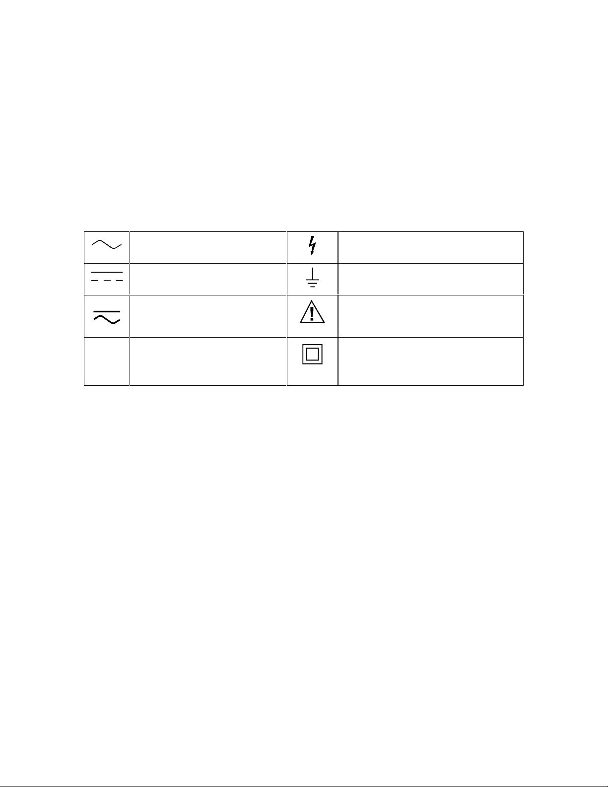
Some common international electrical symbols are shown below:
AC: ALTERNATING CURRENT DANGEROUS VOLTAGE
DC: DIRECT CURRENT EARTH GROUND
EITHER AC OR DC CURRENT SEE EXPLANATION IN MANUAL
X
Before using the meter, read the following safety information carefully. In this manual, "Warning" is
reserved for conditions and actions that pose hazard(s) to the user; "Caution" is reserved for
conditions and actions that may damage your meter.
• Avoid working alone.
• Follow all safety procedures for equipment being tested.
• Inspect the test leads for damaged insulation or exposed metal. Check test lead continuity.
• Be sure the meter is in good operating condition.
• Select the proper function for your measurement.
• To avoid electrical shock, use caution when working above 60V dc or 30V ac rms.
• Disconnect the live test lead before disconnecting the common test lead.
• Disconnect the power and discharge high-voltage capacitors before testing in resistance and
• When making a current measurement, turn the circuit power off before connecting the meter
FUSE
Damaged leads should be replaced.
diodes or continuity.
in the circuit.
DOUBLE INSULATION FOR
PROTECTION AGAINST ELECTRIC
SHOCK
• Check meter fuses before measuring transformer secondary or motor winding current. An
open fuse may allow high voltage build-up, which is potentially hazardous.
• Use clamp-on probes when measuring circuits exceeding 10 amps.
• When servicing the meter, use only the replacement parts specified.
• Do not allow the meter to be used if it is damaged or if its safety features are impaired.
Page 10

Introduction
Service procedures described herein should be performed by
qualified personnel only. To avoid electri c shock, perf orm onl y
those service procedures described in this manual.
The 12B, 18, 7 Series Service Manual provides the information necessary to service the
Fluke Model 12B, Model 18, and Models 7-300 and 7-600 meters. This manual provides
the following information:
Chapter 1
Introduction and Specifications
P
Warning
• Specifications (Chapter 1)
• Basic theory of operation (Chapter 2)
• Disassembly and reassembly (Chapter 3)
• Performance tests (Chapter 3)
• Calibration (Chapter 3)
• Illustrated parts lists and schematic diagrams (Chapter 4)
Refer to the users instruction sheet for operating instructions.
Specifications
Specifications are in Table 1-1. Accuracy is specified for a period of one year after
calibration, at 18ºC to 28ºC (64ºF to 82ºF) with relative humidity to 90%. AC
conversions are ac-coupled, average responding, and calibrated to the rms value of a sine
wave input.
1-1
Page 11

12B/18/7 Series
Service Manual
Accuracy specifications are given as follows:
±([% of reading] + [number of least significant digits])
Table 1-1. Specifications
Maximum Voltage Between any
Terminal and Earth Ground
(excludes 10% tolerance)
Display 3-3/4-digits, 4000 counts, updates 4/sec
Operating Temperature -10°C to 50°C
Storage Temperature -30°C to 60°C indefinitely (to -40°C for 100 hrs)
Temperature Coefficient 0.1 x (specified accuracy)/°C (<18°C or >28°C)
Relative Humidity 0% to 90% (-10°C to 35°C)
Battery Type 9V, NEDA 1604 or IEC 6F22
Battery Life 650 continuous hours with alkaline; 600 hours for Model 7
Shock, Vibration 1 meter shock. Per MIL-T-28800D for a Class 3 Instrument
Size (HxWxL) 1.35 in x 2.75 in x 5.55 in
Weight 10 oz (286g)
EMI Regulations Complies with FCC Part 15, Class B, and VDE 0871B.
Safety
600V ac rms or dc
0% to 70% (35°C to 50°C)
450 continuous hours with carbon-zinc; 400 hours for Model 7
(3.46 cm x 7.05 cm x 14.23 cm)
Designed to Protection Class II requirement of UL1244,
ANSI/ISA-S82.01 - 1988, CSA C22.2 No 231, and VDE 0411, and
IEC 1010-1 overvoltage category III (CAT III), 600V.
1-2
Trademark of TÜV Product Services.
IEC 348 certification; designed to
comply with EN 61010-1: 1993.
Page 12

Introduction and Specifications
Table 1-1. Specifications (continued)
Accuracy (50 to 400 Hz)
Function Range Resolution 7-300 7-600 12B/18
f
E
J
K
LM
1. The 4000 mV range can be entered only in the manual range m ode. Use the 4000 mV range with
accessories. The 4000 mV range i s not available on the Model 7.
2. Not specified for the Model 7.
3. The beeper is guaranteed to come on at <25Ω and t urn off at >250Ω. The meter det ects opens or
shorts of 250 µs or longer. These values are not specified for the Model 7.
4000 mV
4.000V
40.00V
300.0V
400.0V
600.0V
4000 mV
4.000V
40.00V
300.0V
400.0V
600V
400.0Ω
4.000 kΩ
40.00 kΩ
400.0 kΩ
4.000 MΩ
40.00 MΩ
1.000 µF
10.00 µF
100.0 µF
1000 µF
10000 µF
3
2.000V 0.001V NA NA ±(0.9%+2)
1
1
1 mV
0.001V
0.01V
0.1V
0.1V
1V
1 mV
0.001V
0.01V
0.1V
0.1V
1V
0.1Ω
0.001 kΩ
0.01 kΩ
0.1 kΩ
0.001 MΩ
0.01 MΩ
0.001 µF
0.01 µF
0.1 µF
1 µF
10 µF
NA
2
NS
±(2.9%+3)
±(2.9%+3)
NA
NA
NA
2
NS
±(1.5%+1)
±(1.5%+1)
NA
NA
±(1.5%+2)
NA
NA
NA
NA
NA
NA
NA
NA
NA
NA
NA
2
NS
±(2.9%+3)
NA
±(2.9%+3)
±(2.9%+3)
NA
2
NS
±(1.5%+1)
NA
±(1.5%+1)
±(1.5%+1)
±(1.5%+2)
NA
NA
NA
NA
NA
NA
NA
NA
NA
NA
±(1.9%+3)
±(1.9%+3)
±(1.9%+3)
NA
±(1.9%+3)
±(1.9%+3)
±(0.9%+2)
±(0.9%+2)
±(0.9%+1)
NA
±(0.9%+1)
±(0.9%+1)
±(0.9%+2)
±(0.9%+1)
±(0.9%+1)
±(0.9%+1)
±(0.9%+1)
±(1.5%+3)
±(1.9%+2)
±(1.9%+2)
±(1.9%+2)
±(1.9%+2)
±(10%+90)
typical
Specifications
1
1-3
Page 13

12B/18/7 Series
Service Manual
Function
f
E
Overload
Protection
1
600V rms or dc
600V rms or dc
Table 1-1. Specifications (continued)
Common Mode
Rejection Ratio
Input
Impedance
(1 kΩ
Unbalanced)
(Nominal)
>5 MΩ <100pF
2
Automatic Selection
>60 dB at dc 50 or
60 Hz
and LoZ = >2 kΩ
<200pF
(ac coupled)
>10MΩ <100pF
Automatic Selection
and LoZ = >2 kΩ
<200pF
3
2
>100 dB at dc, 50 or
60 Hz
3
2
Normal Mode
Rejection
2
>50 dB at 50 Hz or
60 Hz
Open Circuit
Test Voltage
J
2
L
1. 3 x 10⁶ V Hz maximum.
2. Does not apply to Model 7.
3. ~2 kΩ input impedance up t o 50V. Impedance increases wi th input voltage to >300 kΩ at 600V.
600V rms or dc <1.5V dc <450 mVdc<1.5V dc <500 µA
600V rms or dc 2.4-3.0V dc 2.400V dc 0.95 mA (typical)
Full Scale Voltage
To 4.0 MΩ 40 MΩ
MIN MAX Recording Accuracy and Response Time (Models 12B and 18)
Specified accuracy of the measurement function ±12 digits for changes >200 ms in duration
(±40 digits in ac). Typical 100 ms response to 80%.
MIN MAX Recording with Elapsed Time (Models 12B and 18)
Elapsed Time: 0 to 100 hours (99.59)
Resolution: 1 minute
Accuracy: 0.3 % typical
Continuity Capture (Model 12B)
(Open/Short Capture Model 18)
Detects opens or shorts of 250 µs or longer.
Short Circuit
Current
1-4
Page 14

Introduction
Chapter 2 provides a basic theory of operation for the Models 7, 12B, and 18 Meters.
Electrical components on the printed circuit assembly (A1 Main PCA) are listed in Table
2-1. Refer to Figure 4-3 for the location of these components and Figures 4-4 through
4-7 for the schematic diagrams.
The analog/digital IC (U1) performs the electrical measurement functions. See Table 2-2
for pin names and descriptions. The microcomputer (U2) controls U1, the LCD (U3),
and the user interface. Discrete components support U1 and U2, provide reference
standards for measurements, and provide input overload protection.
Chapter 2
Theory of Operation
Analog Measurement IC (U1)
U1 performs the following analog functions: a/d converter, ac to dc converter,
Automatic Selection circuitry, active filter, passive filter, power supply, range
configuration circuitry, signal routing circuitry, beeper driver, digital control circuitry,
and digital U2 interface circuitry.
The a/d converter is a patented dual-rate, dual-slope converter. The dual-rate conversion
allows for MIN MAX (Models 12B and 18 only) and fast autoranging functions. The ac
to dc converter is full-wave rectified and average-responding. The active and passive
filters are two-pole and one-pole low-pass filters (respectively) that are used for signal
filtering prior to a/d conversion. The internal power supply generates a ground voltage
nominally +3V relative to VSS. Range configuration circuitry connects the Z1 resistor
network as needed for different ranges. Routing circuitry connects the various signal
conditioning circuits as needed. The a/d converter and a counter are controlled by a state
machine.
2-1
Page 15

12B/18/7 Series
Service Manual
Table 2-1. Electrical Components on Main PCA
Circuit and Function Component Designator(s)
Analog Measurement IC
Microcomputer IC
Input Divider and Ohms Reference Resistor Network
Input Divider AC Coupling Capacitor
J2 Input Receptacle Voltage Sense Resistor
J1 Input Receptacle Voltage Sense Resistor
Reference Voltage for Volts Measurements
A/D Converter Integrate Capacitor
A/D Converter Autozero Capacitor
A/D Converter Gain Resistors
Active Filter Components
Passive Filter Components
AC to DC Converter Gain Resistors
AC to DC Converter AC Coupling Capacitor
Bias Current Setting Resistor
DGND-VSS Voltage Setting Resistors
Power Supply Bypass Capacitors
U1
U2
Z1
C14
R17
R14
VR1, R4, R5, R6, R26
C2
C1
R1, R3, R15
R7, R8, C5, C6
R9, C7
R11, R12, R13
C8
R2
R10, R24
C3, C15
Reverse Battery Protection
System Clock
Automatic Selection Input Current Limiters
Automatic Selection Input Positive Temp. Coef. Thermistor
Automatic Selection Input Voltage Clamp Circuit
Automatic Selection Input Fusible Resistor
Microcomputer Reset Circuit
On/Off and Automatic Selection Select Slide Switch
Beeper
Beeper Current Limiter
Slide Switch Protection
Switch Sense Bypass Capacitor
Input Divider Bypass Capacitor
Zero Ohm Jumpers
CR1
Y1
R16, R18, R29
RT1
Q1, Q2, CR2, R28
R19
R23, R25, C10, C13, CR3
S1
LS1
R22
E1
C9
C16
R20, R21, R27
2-2
Page 16
Finally, digital circuitry interfaces with U2 via a parallel address and bidirectional data
bus.
Voltage is measured using a ratio comparison of the unknown voltage to the reference
voltage (REFI pin). Resistance is calculated using a ratio comparison of the voltage
across the unknown resistor to the voltage across a precision reference resistor, with the
same current in both. Capacitance is measured by determining the amount of charge
added for a given dc voltage change.
Microcomputer IC (U2)
U2 writes range settings and a/d converter information to U1. U2 reads a/d converter
results and status information. This includes the low battery check, slide-switch position,
continuity check, and Automatic Selection data. The microcomputer performs math
operations on the raw data from U1 and configures it for the LCD. U2 also reads pushbutton inputs. Finally, the 2.1 MHz clock signal at U2 is divided down to 131 kHz and
sent to U1 (CLK pin) for the counter.
Automatic Selection Input Resistance
Theory of Operation
Microcomputer IC (U2)
2
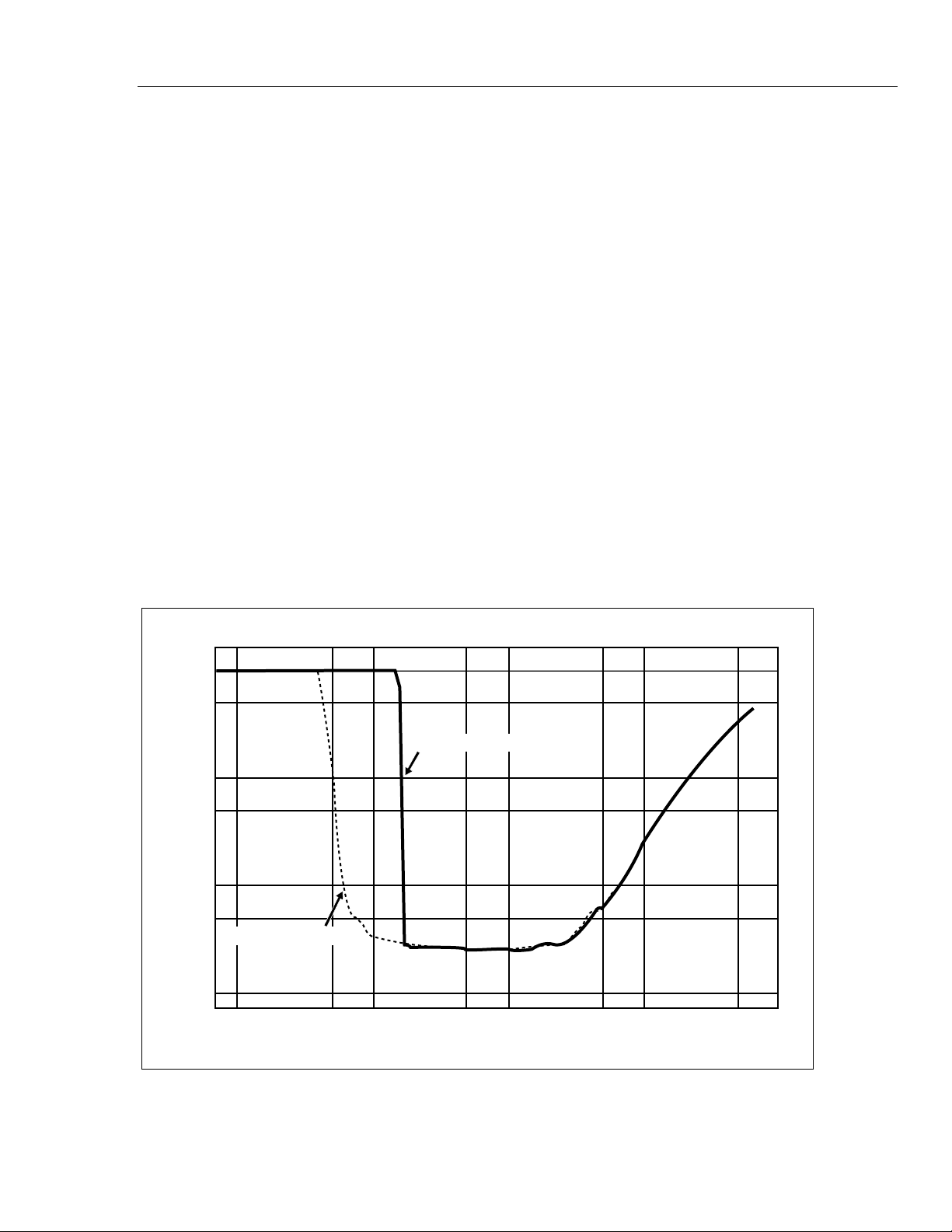
As shown in Figure 2-1, the input resistance for the Automatic Selection function is nonlinear. The data in the graph are for the volts dc function (any range) and are the steady
state values obtained after the PTC thermistor (RT1) has stabilized. The data also apply
for the volts ac function.
500
Positive DCV Input
100
50
10
5
Small Signal Input Tesistance (kΩ)
Negative DCV Input
1
0.1 0.5 1.0 5.0 10.0 50.0 500.0
|Vin| (Vdc)
Figure 2-1. Typical Automatic Selection Input Resistance with DC Volts Function Selected
as01f.eps
2-3
Page 17

12B/18/7 Series
Service Manual
Table 2-2. U1 Pinout Table
Pin No. Pin Name Description
1 READ (L) When low (VSS), data from addressed register can be read
2 ADR5 Most significant address bus line
3 ADR4 Bit 4 of parallel address bus
4 ADR3 Bit 3 of parallel address bus
5 ADR2 Bit 2 of parallel address bus
6 ADR1 Bit 1 of parallel address bus
7 ADR0 Least significant address bus line
8 VSS Negative power supply voltage (-3V relative to DGND)
9 VDD Positive power supply voltage for analog only (Vbat-3V=VDD-DGND)
10 K0 1st a/d gain resistor pin, generally for de-integrate
11 K1 2nd a/d gain resistor pin, generally for integrate
12 K2 3rd a/d gain resistor pin, for autozero
13 AZ A/D converter pin for autozero capacitor
14 INT A/D converter pin for integrator capacitor
15 REFI 1.00V reference voltage for de-integrate signal in volts
16 BIAS Pin for analog bias current generator reference resistor
17 REFH Connects 1.235V reference voltage to on-chip circuits
18 BGND Not used
19 AFO Active filter high output pin (2-pole, low-pass filter)
20 FAO Internal active filter node
21 FAI Internal active filter node
22 AFI Active filter high input pin
23 VSS Negative power supply voltage (-3V relative to DGND)
24 PFO Passive filter low output pin (1-pole, low-pass filter)
25 AVAOM Absolute value amp (full wave rectified) negative output pin
26 AVAOP Absolute value amp (full wave rectified) positive output pin
27 AVAM Absolute value amp inverting input (summing node)
28 ACBO AC buffer output
29 VSET Voltage divider sense for power supply
30 PSTEST Pin to disable on-chip power supply for U1 testing
31 DGND Ground power supply pin connected to common (digital ground)
32 AGND Common input sense line. No current flow (analog ground).
33 CLAMP Op amp output voltage for Q2 clamp transistor base drive
34 AMPS Shunt resistor sense pin. Unused in Fluke Model 18.
35 ISRC Current source pin for continuity, ohms, and capacitance
36 SWS Slide-switch position sense pin. Internal pull down.
37 OHMS Ohms sense resistor input pin. Sense voltage at J2.
38 VSS Negative power supply voltage (-3V relative to DGND)
39 ACV AC volts input pin from 10 MΩ resistor
2-4
Page 18

Automatic Selection Input Resistance
Table 2-2 U1 Pinout Table (continued)
Pin No. Pin Name Description
40 APV0 DC volts input pin from 10 MΩ resistor
41 DIVLO Input divider (Z1) common (low) pin
42 APV1 10-to-1 voltage divider and 1 MΩ reference resistor input
43 APV2 100-to-1 voltage divider and 100 kΩ reference resistor input
44 APV3 1000-to-1 voltage divider and 10 kΩ reference resistor input
45 APV4 10,000-to-1 voltage divider and 1 kΩ reference resistor input
46 GND Ground power supply pin connected to common (digital ground)
47 DATA3 Most significant bidirectional data bus line
48 DATA2 Bit 2 of parallel data bus
49 DATA1 Bit 1 of parallel data bus
50 DATA0 Least significant bidirectional data bus line
51 N/C No connection
52 BEEPER (L) One of two beeper drive lines. Voltage swings VDD to VSS.
53 VSS Negative power supply line (-3V relative to DGNG)
54 VSS Negative power supply line (-3V relative to DGNG)
55 CLK System clock line from U2. 131,072 Hz.
56 BCLK Beeper frequency (2.3 kHz) clock line from U2
57 TESTCLK Test clock pin for U1 testing
58 BEEPER One of two beeper drive lines. Voltage swings VDD to VSS.
59 N/C No connection
60 WRITE (L) When driven low (VSS), data is written to addressed register
Theory of Operation
2
2-5
Page 19

12B/18/7 Series
Service Manual
2-6
Page 20

static awareness
A Message From
Fluke Corporation
Some semiconductors and custom IC's can be
damaged by electrostatic discharge during
handling. This notice explains how you can
minimize the chances of destroying such devices
by:
1. Knowing that there is a problem.
2. Leaning the guidelines for handling them.
3. Using the procedures, packaging, and
bench techniques that are recommended.
The following practices should be followed to minimize damage to S.S. (static sensitive) devices.
1. MINIMIZE HANDLING
2. KEEP PARTS IN ORIGINAL CONTAINERS
UNTIL READY FOR USE.
3. DISCHARGE PERSONAL STATIC BEFORE
HANDLING DEVICES. USE A HIGH RESIS TANCE GROUNDING WRIST STRAP.
4. HANDLE S.S. DEVICES BY THE BODY.
Page 21

5. USE STATIC SHIELDING CONTAINERS FOR
HANDLING AND TRANSPORT.
6. DO NOT SLIDE S.S. DEVICES OVER
ANY SURFACE.
8. WHEN REMOVING PLUG-IN ASSEMBLIES
HANDLE ONLY BY NON-CONDUCTIVE
EDGES AND NEVER TOUCH OPEN EDGE
CONNECTOR EXCEPT AT STATIC-FREE
WORK STATION. PLACING SHORTING
STRIPS ON EDGE CONNECTOR HELPS
PROTECT INSTALLED S.S. DEVICES.
9. HANDLE S.S. DEVICES ONLY AT A
STATIC-FREE WORK STATION.
7. AVOID PLASTIC,VINYL AND STYROFOAM
IN WORK AREA.
PORTIONS REPRINTED
WITH PERMISSION FROM TEKTRONIX INC.
AND GERNER DYNAMICS, POMONA DIV.
Dow Chemical
10. ONLY ANTI-STATIC TYPE SOLDER SUCKERS SHOULD BE USED.
11. ONLY GROUNDED-TIP SOLDERING
IRONS SHOULD BE USED.
Page 22

Introduction
Chapter 3 covers the following:
• Disassembly and reassembly
• Cleaning
• Performance tests
• Calibration
Chapter 3
Maintenance
Disassembly and Reassembly
P
To avoid electrical shock, remove test leads and any input
signals before opening the case.
Caution
To avoid contamination from the fi ngers, handle the pca by the
edges or wear gloves. PCA contamination can cause failures in
humid environments. This meter contains components that can
be damaged by static discharge. To avoid damaging these
components when servicing the meter, take precautions
indicated on the "Static Awareness" at t he beginning of
Chapter 3.
Warning
3-1
Page 23

12B/18/7 Series
Service Manual
Referring to Figures 3-1 and 3-2 as necessary, disassemble the meter as follows. A
Phillips-head screwdriver and small flat-blade screwdriver are required.
1. Remove the test leads and set the slide switch or rotary knob to OFF.
2. Remove the Phillips-head screws (H1-4) from the case bottom (MP8).
3. Separate the case top (MP2) from the case bottom.
4. TO REPLACE THE BATTERY: Lift the battery from the case bottom and insert a
new 9V battery (NEDA 1604, 6F22, or 006P). Be sure the positive and negative
battery posts are oriented correctly.
5. TO REMOVE THE PCA (A1): Insert a small, flat-blade screwdriver between the
edge of the case top and the pca where shown in Figure 3-3. Gently unsnap a side of
the case top from the pca. Repeat on the other side of the pca. Unsnap the case from
the top of the pca last.
6. LIFT THE PCA FROM THE CASE TOP BY ITS EDGES. If the elastomeric contact
strips (J3, J4)
*
for the switch assembly (S2)* and LCD (U3) are stuck to the pca,
remove them without touching the conductive edges.
TO REINSERT THE PCA: Important: First make sure that the slide-switch
actuator (MP5), the slide switch (S1), and the rotary knob (for the 12B and 18) are
in the OFF position. Place the pca over the four screw posts in the case top, then
press gently on the center of the pca while using the small flat-edge screwdriver to
shoehorn the pca under the snap on a side of the case top. Repeat on the other side
and the top.
7. TO REMOVE THE SWITCH SUPPORT (MP6): Use a small, flat-blade
screwdriver to gently unsnap the sides and top of the switch support from the snaps
shown in Figure 3-3.
8. The LCD, switch assembly, slide-switch actuator, and elastomeric contact strips
(J3, J4) for the LCD and switch assembly are accessible and can be replaced as
needed. Do not allow the LCD to get wet. Before installing a new LCD, make sure
that all connector contact points are clean.
Caution
Do not touch the conductive edges of the elastomeri c strips or
the contacts on the switch assembly. If they are contaminated,
clean them with isopropyl alcohol .
9. Reassembling the meter is the reverse of disassembling it. After the meter is
reassembled, execute the PERFORMANCE TESTS to confirm that the meter is
working properly.
3-2
*
J4 and S2 are not present in Mode ls 7-300 and 7-600.
Page 24

Switch Assembly
Actuator, Switch
Disassembly and Reassembly
Case, Top
LCD
Conn.
Elastomeric
Conn.
Elastomeric
LCD to PCA
Support, Switch Assembly
Maintenance
3
Main PCA
Shield, Bottom
Battery
Shock Absorber
Case, Bottom
Screw, THD Form, PH.P.STL,
5-14 x .750
Foot
Figure 3-1. Models 12B and 18 Disassembled Unit
as07f.eps
3-3
Page 25

12B/18/7 Series
Service Manual
Case, Top
LCD
Conn.
Elastomeric
LCD to PCA
Actuator Switch
Support,
Switch Assembly
Main PCA
Shield, Bottom
Foot
Shock Absorber
Battery
Case, Bottom
Screw, THD Form, PH.P.STL,
5-14 x .750
3-4
Figure 3-2. Models 7-300 and 7-600 Disassembled Unit
as10f.eps
Page 26

2
Maintenance
Disassembly and Reassembly
3
3
Snap
Snap
Snaps
1
Figure 3-3. Removing and Reinserting the Printed Circuit Assembly
as04f.eps
3-5
Page 27

12B/18/7 Series
Service Manual
Cleaning
Performance Tests
Caution
To avoid damaging the meter, do not use aromatic
hydrocarbons or chlorinated solvents for cleaning. These
solutions will react with the plastics used in the instruments.
Do not get the LCD wet.
To clean the case, wipe it with a cloth lightly dampened with water and a mild detergent.
Wash the pca with isopropyl alcohol or hot deionized water and a soft brush. Do not use
detergent of any kind for cleaning the pca. The pca must be completely dry before the
meter is reassembled. Dry the pca with clean dry air at low pressure (<20 psi); then bake
it at 50ºC for 2 hours.
P
Warning
To avoid electric shock, do not execute the performance t est s
procedures unless the meter is fully assembled.
Use the PERFORMANCE TESTS to confirm that the meter is working properly. If the
meter fails any of these tests, it needs calibration (see CALIBRATION) or repair. The
equipment required is specified in Table 3-1.
1. Connect the calibrator to the [+] and COM jacks on the meter.
2. Referring to Table 3-2 for the Fluke 7-300 or 7-600, or Table 3-3 for the Fluke 12B
or 18, put the meter in the function and range shown for Test 1.
3. Apply the input from the appropriate source. The reading on the display should be
within the MINIMUM and MAXIMUM values shown in Table 3-2 or 3-3.
4. Test the remaining functions and ranges.
Table 3-1. Required Equipment
Equipment Minimum Specifications Recommended Models
DMM Calibrator DC Voltage: 0-600V
Accuracy: ±0.25%
AC Voltage: 0-600V
Accuracy: ±0. 5%
Frequency: 50-400 Hz
Decade Resistor Resistance: 1.0-40 MΩ
Accuracy: ±0. 25%
Fluke Models 5700A, 5500A,
5100B, or equivalent
General Resistance RDS-77B
and 41B or Fluke 5500A
3-6
Decade Capacitor Capacitance: 0-1.000 µF
Accuracy: ±0. 5%
GenRad 1412-BC or Fluke 5500A
Page 28

Table 3-2. Performance Tests for Models 7-300 and 7-600
Maintenance
Performance Tests
3
Test No. Applicable
Model(s)
1
2
3
4
5
6
7
8
9
10
11
12
7-300/7-600
7-300/7-600
7-300/7-600
7-300/7-600
7-300/7-600
7-300
7-600
7-600
7-300/7-600
7-300/7-600
7-300/7-600
7-300/7-600
1
Meter
Range
40.00V ac
40.00V ac
40.00V ac
400.0V ac
(300.0V ac for
7-300)
400.0V ac
(300.0V ac for
7-300)
300V ac
400.0V ac
600V ac
40.00V dc
40.00V dc
400.0V dc
400.0V dc
(300.0V dc for
7-300)
Input To
Meter
4.40V, 50 Hz
35V, 50 Hz
35V, 400 Hz
100V, 50 Hz
150V, 400 Hz
300V, 50 Hz
350V, 80 Hz
600V, 400 Hz
4.40V dc
-35V dc
+100V dc
-150V dc
Display
Minimum
4.24
33.95
33.95
96.8
145.4
291
339.5
580
4.32
-35.54
+98.4
-152.3
Display
Maximum
4.56
36.05
36.05
103.2
154.6
309
360.5
620
4.48
-34.46
+101.6
-147.7
13
14
2
15
2
16
3
17
1. To avoid overload/current lim i t condition on the calibrator when t esting the Model 7, defeat t he 50Ω divider on the
calibrator and allow at least 3 seconds at each voltage i nterval above 40V.
2. Model 7 beeper should be on.
3. Model 7 beeper may be on or off.
7-300/7-600
7-600
7-300/7-600
7-300/7-600
7-300/7-600
400.0V dc
(300.0V dc for
7-300)
600V dc
400.0Ω
400.0Ω
400.0Ω
300V dc
-600V dc
0.0Ω
1.0Ω
350.0Ω
295.4
-610
0.0
0.8
344.5
304.6
-590
0.2
1.2
355.5
3-7
Page 29

12B/18/7 Series
Service Manual
Table 3-3. Performance Tests for Models 12B and 18
Test
No.
1
2
3
4
5
6
7
8
2
9
10
11
12
13
14
15
16
17
18
19
20
21
22
23
24
25
26
27
28
29
30
31
32
1. Center position for Model 18.
2. In the Automatic Sel ection mode, the UUT uses a low-i m pedance thermistor (~2.5k f or circuit protection and l oad
testing (referred to as low-Z input circuitry). When usi ng the 5100B, 5500A, or 5700A to drive the UUT with high
voltages, avoid an overload/current limit condition by gradually stepping t he voltage up (waiting two seconds
between each step) from 90.0V, 120.0V, 180.0V, and 350.0V at 80 Hz each step.
3. Calibrator 50Ω divider override.
4. The dc volts annunciator m us t be on. Test does not apply t o Model 18.
(Automatic Selection 12B Only)
4.000V ac
4.000V ac, MIN MAX
4.000V ac
4.000V ac
4.000V ac
4.000V ac
40.00V ac
40.00V ac
400.0V ac
600V ac
4.000V dc, MIN MAX
4.000V dc
40.00V dc
400.0V dc
4.000V dc
40.00V dc
400.0V dc
600V dc
Continuity
3
Continuity, Automatic Selection
3
Continuity, Automatic Selection
400.0Ω
400.0Ω
400.0Ω
4.000 kΩ
40.00 kΩ
400.0 kΩ
4.000 MΩ
40.00 MΩ
Ω, Automatic Selection
5
1.000 µF
5
1.000 µF
Meter Range
Input To
Meter
0V
0V
10 mV, 50 Hz
10 mV, 400 Hz
3.5V, 50 Hz
3.5V, 400 Hz
35V, 50 Hz
35V, 400 Hz
350V, 80 Hz
600V, 400 Hz
0V
0V
+20 mV dc
-200 mV dc
+3.5V
-35V dc
+100V dc
-600V dc
3
+2V dc
+3.43V dc
-0.5V dc
3
3
0.0Ω
1.0Ω
350.0Ω
1.0 kΩ
35 kΩ
100 kΩ
2.9 MΩ
35 MΩ
1.96V dc
0.0 µF
0.95 µF
Switch
Position
Center
Center
Center
1
Right
1
Right
Center
Center
Right1
1
Right
Center
Center
1
Right
1
Right
Center
Center
Center
Center
Center
Right
Right
Right
Right
Right
Right
Right
Right
Right
Right
Right
Right
Right
Right
Display
Minimum
0.000
0.000
0.007
0.007
3.430
3.430
34.30
34.30
343.0
586
-0.012
-0.002
00.01
-000.3
+3.466
-35.33
+99.0
-606
1.980
4
3.397
4
-0.507
0.0
0.8
346.6
0.990
34.67
99.0
2.873
34.44
4
1.940
-0.001 µF
0.930 µF
Display
Maximum
0.003
0.040
0.013
0.013
3.570
3.570
35.70
35.70
357.0
614
0.012
0.002
00.03
-000.1
+3.534
-34.67
+101.0
-594
2.020
4
3.463
4
-0.493
0.2
1.2
353.4
1.010
35.33
101.0
2.927
35.56
4
1.980
0.001 µF
0.970 µF
5. Conducting performance tests of t he 400Ω, 4 kΩ, 40 kΩ, and 1 µF ranges (tes ts no. 22, 23, 24, 25, 26, 31, and 32)
verifies that the discrete and integrated circui try needed to support the other capacitance ranges are working withi n
specifications. Therefore, the tests indirectly verify that the meter will meet specification in the 10 µF, 100 µF,
1000 µF, and 10,000 µF ranges.
3-8
Page 30

Calibration Adjustments for Models 12B and 18
Calibration Adjustments for Models 12B and 18
To ensure that the meter performs to specifications, make calibration adjustments
annually using the following procedure:
1. Set the calibrator for 0V dc. Put the meter in the 4.000V dc range.
2. Connect the calibrator to the [+] and COM jacks on the Meter.
3. Apply an input of +4.000V dc ±0.25%
The meter display should read between 3.997-4.003V. If it does not, adjust R4 (see
Figure 3-4) as described below.
To adjust R4, proceed as follows:
1. Remove any input signals to the meter.
2. Remove the four screws on the back and separate the case bottom and case top.
Notice that when you do so the battery remains in the case bottom and power to the
meter is disconnected.
3. Observing correct polarity, connect a 9V battery to the battery contacts using easy
hook jumpers or alligator clip leads (see Figure 3-4).
Maintenance
3
Note
To avoid stretching or bending the battery contacts, connect leads to the
base of the contacts as shown in Figure 3-4.
4. Set the calibrator for 0V dc. Put the meter in the 4.000V dc range.
5. Connect the calibrator to the [+] and COM jacks on the meter.
6. Apply an input of +4.000V dc ±0.25%
7. Adjust R4 (see Figure 3-4) so that the meter display reads between 3.997 and
4.003V.
3-9
Page 31

12B/18/7 Series
Service Manual
Clip to Base Contacts
+
Input Receptacles
+
+
9V
Adjust R4 for 3.997-4.003V DC
Figure 3-4. Calibration Adjustment
BATTERY
Calibration Adjustments for Models 7-300 and 7-600
To ensure that the meter performs to specifications, make calibration adjustments
annually using the following procedure:
1. Set the calibrator for 0V dc. Switch the meter ON.
2. Connect the calibrator to the [+] and COM jacks on the meter. Defeat the 50Ω
divider on the calibrator (if any).
3. Apply an input of 3.500V dc ±0.25%. Wait at least 3 seconds.
4. Apply an input of 3.75V dc ±0.25%. Within 5 seconds the meter should display a
reading between 3.747 and 3.753V dc. If it does not, adjust R4 as described below.
_
as05f.eps
3-10
To adjust R4, proceed as follows:
1. Remove any input signal to the meter.
2. Remove the four screws on the back and separate the case bottom from the case top.
Notice that when you do so, the battery remains in the case bottom and power to the
meter is disconnected.
3. Observing the correct polarity, connect a known good 9V battery to the battery
contacts using easy-hook jumpers or alligator clip leads. Refer to Figure 3-4.
Note
To avoid stretching or bending the battery contacts, connect the leads to
the base of the contacts, as shown in Figure 3-4.
4. Set the calibrator for 0V dc. Turn the meter ON.
Page 32

Maintenance
Calibration Adjustments for Models 7-300 and 7-600
5. Connect the calibrator to the [+] and COM input jacks on the meter. Defeat the 50Ω
divider on the calibrator (if any).
6. Apply an input of 3.500V dc ±0.25%. Wait at least 3 seconds.
7. Apply an input of 3.75V dc ±0.25%. Wait 5 seconds.
8. Adjust R4 so that the meter displays a reading between 3.747 and 3.753V dc.
9. Remove the inputs to the meter, disconnect the battery, and reassemble the meter.
3
3-11
Page 33

12B/18/7 Series
Service Manual
3-12
Page 34

Introduction
This chapter contains an illustrated list of replaceable parts for the 7-300, 7-600, 12B,
and 18 Meters. Parts are listed by assembly; alphabetized by reference designator. Each
assembly is accompanied by an illustration showing the location of each part and its
reference designator. The parts lists give the following information:
• Reference designator
• An indication if the part is subject to damage by static discharge
• Description
• Fluke stock number
• Total quantity
• Any special notes (i.e., factory-selected part)
Chapter 4
Parts and Schematics
A * symbol indicates a device that may be damaged by static
discharge.
How to Obtain Parts
Electrical components may be ordered directly from the manufacturer by using the
manufacturers part number, or from the Fluke Corporation and its authorized
representatives by using the part number under the heading FLUKE STOCK NO. In the
U.S., order directly from the Fluke Parts Dept. by calling 1-800-526-4731. Parts price
information is available from the Fluke Corporation or its representatives. Prices are also
available in a Fluke Replacement Parts Catalog which is available on request.
In the event that the part ordered has been replaced by a new or improved part, the
replacement will be accompanied by an explanatory note and installation instructions, if
necessary.
Caution
4-1
Page 35

12B/18/7 Series
Service Manual
Manual Status Information
Ref. or Option No. Assembly Name Fluke Part No. Revision Level
To ensure prompt delivery of the correct part, include the following information when
you place an order:
• Instrument model and serial number
• Part number and revision level of the pca containing the part.
• Reference designator
• Fluke stock number
• Description (as given under the DESCRIPTION heading)
• Quantity
The Manual Status Information in Table 4-1 defines the assembly revision levels that are
documented in the manual. Revision levels are printed on each pca.
Table 4-1. Manual Status Information
A1 PCB ASSEMBLY (FLUKE 12) 879002 M
A1 PCB ASSEMBLY (FLUKE 10/18) 878991 M
A1 PCB ASSEMBLY (FLUKE 7-300) 614963 M
A1 PCB ASSEMBLY (FLUKE 7-600) 614966 M
Newer Instruments
Changes and improvements made to the instrument are identified by incrementing the
revision letter marked on the affected pca. These changes are documented on a manual
supplement sheet which, when applicable, is included with the manual.
Parts Lists, Drawings, and Schematics
This section contains the parts lists, drawings, and schematics for the meters.
Note
This instrument may contain a Nickel-Cadmium battery. Do not mix with
the solid waste stream. Spent batteries should be disposed of by a qualified
recycler or hazardous materials handler. Contact your authorized Fluke
service center for recycling information.
P
Warning
To avoid fire or explosion, replace the fusible resistor only with
Fluke PN 867361.
4-2
Page 36

Parts Lists, Drawings, and Schematics
Table 4-2. Models 12B, 18, and 18/AL Final Assembly
Parts and Schematics
4
Reference
Designator Description
A1 MAIN PCA (MODEL 12B) 879002 1
A1 MAIN PCA (MODEL 18) 878991 1
BT1 BATTERY, 9V, 0-15MA 696534 1
H1-4 SCREW, PH, P, AM THD FORM , STL, 5-14, .750 832246 4
J3 CONN, ELASTOMERIC, LCD TO P WB, 2.050 L 867247 1
J4 CONN, ELASTOMERIC, S WITCH TO PWB, .500 L 867242 1
MP2 CASE TOP, (PAD XFER & WINDOW, MODEL 12B) 614948 1
MP2 CASE TOP, (PAD XFER & WINDOW, MODEL 18) 614955 1
MP2 CASE TOP, (PAD XFER & WINDOW, MODEL 18/AL) 615192 1
MP5 ACTUATOR, SWITCH 203445 1
MP6 SUPPORT, SWITCH ASSEMBLY 879031 1
MP8 CASE, BOTTOM, YELLOW (MODEL 12B) 614864 1
MP8 CASE, BOTTOM, GRAY (MODEL 18) 614872 1
MP9 SHIELD, BOTTOM 878277 1
MP10 SHOCK ABSORBER 878983 1
MP11 FOOT, NON-SKID 885884 1
MP12 TEST LEADS 855742 1
S2 SWITCH ASSEMBLY (MODEL 12B) 614799 1
S2 SWITCH ASSEMBLY (MODEL 18) 614807 1
U3 LCD, 3.5 DIGIT, MULTIPLEXED 855226 1
TM1 12B/18 INSTRUCTION SHE E T 602000 1
Fluke Stock
Number
Total
Quantity
4-3
Page 37

12B/18/7 Series
Service Manual
MP2
U3
J4
J3
S2
MP5
MP6
A1
MP9
BT1
MP10
MP8
H1-4
4-4
MP11
FLUKE 12B, FLUKE 18, FLUKE 18/AL
T&B
as06f.eps
Figure 4-1. Models 12B and 18 Final Assembly
Page 38

Parts Lists, Drawings, and Schematics
Table 4-3. Models 7-300 and 7-600 Final Assembly
Parts and Schematics
4
Reference
Designator Description
A1 MAIN P CA (M ODEL 7-600) 614966 1
A1 MAIN P CA (M ODEL 7-300) 614963 1
BT1 BATTERY, 9V, 0-15MA 696534 1
H1-4 S CRE W, PH, P, AM THD FORM, S T L, 5-14, .750 832246 4
J3 CONN, ELASTOMERIC, LCD TO P WB , 2.050 L 867247 1
MP2 CASE TOP, (PAD XFER & WINDOW, MODEL 7-600) 614930 1
MP2 CASE TOP, (PAD XFER & WINDOW, MODEL 7-300) 614922 1
MP5 ACTUATOR, SWITCH 203452 1
MP6 SUPPORT, SWITCH ASSEMBLY 879031 1
MP8 CASE, BOTTOM, YELLOW 614864 1
MP9 SHIELD, BOTTOM 878277 1
MP10 SHOCK ABSORBER 878983 1
MP11 FOOT, NON-SKID 885884 1
MP12 TEST LEADS 855742 1
U3 LCD, 3.5 DIGI T, MULTIPLEXED 855226 1
TM1 INSTRUCTI ON SHEET, FLUKE 7 602018 1
Fluke Stock
Number
Total
Quantity
4-5
Page 39

12B/18/7 Series
Service Manual
MP2
U3
J3
MP5
MP6
A1
MP9
MP11
MP10
BT1
MP8
H1-4
4-6
FLUKE 7-300, FLUKE 7-600
T&B
as09f.eps
Figure 4-2. Models 7-300 and 7-600 Final Assembly
Page 40

Parts and Schematics
Parts Lists, Drawings, and Schematics
Table 4-4. A1 Main PCA
Fluke
Reference
Designator Description Number 7-300 7-600 12B 18
C1 CAP, TA, 0.47 µF, ±20%, 35V 655035 1 1 1 1
C2, C5-7 CAP, POLYES, 0.022 µF, ±10%, 50V 715268 0 0 4 4
C2, C7 CAP, POLYES, 0.022 µF, ±10%, 50V 715268 2 2 0 0
C3 CAP, TA, 22 µF, ±20%, 6V, 6032 876545 1 1 1 1
C4, C13 CAP, CE R, 0.1 µF, ±10%, 25V, X7R, 1206 747287 0 2 2 0
C4, C12, C13 CAP, CER, 0.1 µF, ±10%, 25V, X7R, 1206 747287 3 0 0 0
C4, C11, C13 CAP, CER, 0.1 µF, ±10%, 25V, X7R, 1206 747287 0 0 0 3
C5, C6 CAP, CER, 4700 PF, ±20% , 100V 743427 2 2 0 0
C8 CAP, TA, 3.3 µF, ±20%, 16V, 3528 876552 1 1 1 1
C9 CAP, CER, 0.022 µF, ±10%, 50V, X 7R, 1206 747279 1 1 1 1
C10 CAP, AL, 22 µF, ±20%, 10V, SOLV PROOF 887245 1 1 1 1
C14 CAP,POLY,.01 µF, ±10%,.1000V 822361 1 1 1 1
C15 CAP, TA, 47 µF, ±20%, 10V, 7343 867580 1 1 1 1
C16 CAP, CER, 10 PF, ±20%, 50V, C0G 721589 1 1 1 1
CR1 DIODE , SI, 100 PIV, 1 AMP, SURFACE MOUNT 912451 1 1 1 1
CR2 DIODE,SI,DUAL, BV = 50V , IO = 100 mA, SOT-23 851659 1 1 1 1
CR3 DIODE,SI, BV = 70V, I O = 50 m A, DUAL, SOT-23 742320 1 1 1 1
E1 SURGE PROTECTOR, 3750v,±20% 867361 1 1 1 1
J1, J2 RECEPTACLE, INPUT 878988 2 2 2 2
LS1 AF TRANSD, PIEZO, 20MM 876995 1 1 1 1
Q1 TRANSISTOR, SI, NPN, SELECT IEBO, S O T-23 821637 1 1 1 1
Q2 TRANSISTOR, SI, PNP, SELECT ICER, SOT-23 887179 1 1 1 1
R1 RES, CERM, 162K, ±1% , .125W, 100 PPM, 1206 876198 1 1 1 1
R2 RES, MF, 332K, ±1%, 0.125W, 100 PPM 655217 1 1 1 1
R3 RES, MF, 23.4K, ±0.1%, 0.125W, 100 PPM 876292 1 1 1 1
R4 RES,VAR,CERM,25K , ±25%,.2W 876300 1 1 1 1
R5 RES, CERM, 43.2K, ±1% , .125W, 100 PPM, 1206 887109 1 1 1 1
R6 RES, CERM, 226K, ±1% , .125W, 100 PPM, 1206 876524 1 1 1 1
R7-9, R23, R28 RES, CERM, 1M, ±1% , .125W, 100 PPM, 1206 836387 5 5 5 5
R10 RES, CERM, 309K, ±1%, .125W, 100 P PM, 1206 876201 1 1 1 1
R11, R12 RES, MF, 30.1K, ±0.1%, 0.125W, 100 P PM 887161 2 2 2 2
R13 RES, MF, 27.1K, ±0.1%, 0.125W, 100 PPM 876289 1 1 1 1
R14, R15 RES, CERM, 10K, ±5%, .125W, 200 PPM, 1206 746610 2 2 2 2
R16, R18 RES,CERM, 470, ±5%,3W 887117 2 2 2 2
R17 RES,CERM, 1M, ±5%,1W 912589 1 1 1 1
R19 RES, MF, 450, ±10%, 107398 1 1 1 1
R21 RES J UMPER, 0.02, 0.25W 682575 1 1 1 1
R22, R29, R30 RES, CERM, 300, ±5%, . 125W, 200 PPM, 1206 746362 3 3 3 3
R24 RES, CERM, 487K, ±1%, .125W, 100 P PM, 1206 887112 1 1 1 1
R25 RES, CERM, 2.2M, ±5%, . 125W, 200 PPM, 1206 811778 1 1 1 1
Stock Total Quantity
4
4-7
Page 41

12B/18/7 Series
Service Manual
Reference
Designator Description Number 7-300 7-600 12B 18
R26 RES, CE RM, 100K, ±1%, .125W, 100 P P M, 1206 769802 1 1 1 1
R27 RES, CERM, 0, +.05 MAX, .125W, 1206 810747 1 1 1 1
RT1 THERM, POS 1.1K, ±20% , 25C 867192 1 1 1 1
S1 SWITCH, SLIDE, 3 POS, 5 PI N 868117 1 1 1 1
U1 ARTIC, ASSEMBLY TESTED 858472 1 1 1 1
U2 IC, CMOS, 4 BIT MPU, LCD 601575 1 1 0 0
U2 *IC, CMOS, 4 BIT MPU, LCD CNTRLR, 80PNQFP 866913 0 0 1 1
VR1 IC, 1.23V, 150 PPM T.C., BANDGAP V . REF 634451 1 1 1 1
XBT, XBT2 CONTACT, BATTERY 890327 2 2 2 2
Y1 RESONATOR, CERAMIC, P IEZOELEC, 2.10
Z1 RES NET THK FILLM TESTED 872234 1 1 1 1
MHZ
Table 4-4. A1 Main PCA (cont)
Fluke
Stock
876024 1 1 1 1
Total Quantity
4-8
Page 42

Parts and Schematics
Parts Lists, Drawings, and Schematics
4
FLUKE 12-1601
Figure 4-3. Models 12B, 18, 7-300, and 7-600 Main PCA Components
as11f.eps
4-9
Page 43

12B/18/7 Series
Service Manual
ADR0
CLK
ADR1
READ*
WRI T E*
VDD
ADR5
ADR4
ADR3
ADR2
BCLK
VSS1
VBT+
DATA0
DATA1
DATA2
VSS2
DGND
DATA3
VSS2
9V
BT1
CR1
1N4002
T
6V
22
C3
20%
(1 of 2)
FLUKE 12-1201
LS1
0
20
R27
R22
300
4
8
Z1
1. 00K
Z1
4
7
10. 01K
Z1
6
4
101K
Z1
4
5
1. 111M
APV0
ACV
50V
C16
10pF
VSS2
DGND
SWS
Q2
AGND
ISRC
R28
1M
1%
300
R29
T
10V
C15
20%
Q1
47
VDD
CR2
BAV74
1M
1W
DGND
DGND
10%
50V
C9
.022
.01
M
1KV
C14
VDD
R30
300
32541
VBT+
Z1
10. 0M
21
Z1
10. 0M
23
VOLT/ OHMS
R8
M
54
VSS
AFI
22
VSS1
1M
1%
52
50
4948473146
51
53
N/ C
VSS
BEEPER*
DATA2
DATA1
DATA0
APV4
APV3
DGND
DATA3
44
APV2
APV1
DI VL O
41
APV0
ACV
39
VSS
U1
38
OHMS
37
SWS
36
ISRC
35
AMPS
CLAMP
33
AGND
32 34 40 42 43 45
DGND
PSTEST
VSET
ACBO
AVAM
AVAOP
AVAOM
PFO
VSS
28
1%
272526
AVAOM
C7
.022
50V M
R13
C8
30
29
R11
30. 1K
MF
0. 1%
OHMS
MF
20%
0
R21
TP9
DGND
5%
MG
5
470
R16
3W
27. 1K
0. 1%
T
3. 3
16V
24
23
R9
1M
R17
30. 1K
MF
0. 1%
R12
R24
487K
R10
1%
309K
1%
TP7
TP8
DGND
R14
10K
TP6
J1
COMMON
5%
MG
R19
470
5
3W
5%
R18
MG
5
470
3W
t
RT1
+
5
20%
1. 1K
AGND
E1
S1
20%
3750V
BOTTOM SHI ELD
J2
60
1
59
READ*
N/ C
ADR5
WRI T E*
ADR4
5818
BEEPER
56
55
57
CLK
BCLK
TESTCLK
ADR3
ADR2
ADR1
ADR0
765432
VSS
8
VDD
0. 1%
MF
23. 4K
R3
9
K0
101112
K1
K2
AZ
1%
10K
R15
R1
162K
35V
C1
.47
20%
50V
C2
. 022
13
INT
14
REFI
15
BGND
REFH
BI AS
16
17
FAI
FAO
AFO
19
21
20
T
332K
R2
1%
MF
M
TP5
FAO
AFO
FAI
BGND
CW
25%
25K
R4
REFI
R7
VDD
R26
100K
1%
VR1
1. 235V
REFH
R5
43. 2K
1%
R6
226K
1%
TP4
1M
1%
M
C6
50V
. 022
50V
C5
. 022
TOP SHI ELD
as20f.eps
Figure 4-4. Model 12B Schematic
4-10
Page 44

Parts and Schematics
Parts Lists, Drawings, and Schematics
CARBON FI L MCF
CARBON COMPCC
MET A L GL AZ E
WI RE WOUND
METAL FI LM
MGWWMF
SELECT
S2
1
MEMBRANE TAI L
PIN ASSIGNMENTS
RANGE
26543
VSS
VSS
10%
0. 1
C13
AL UMI NUMAL
POLYPROPYLENE FI LM
MYLAR/ POLYESTER
CERAMI C
TANTAL UM
MCTPCPP
SY M CAPACITOR SYM RESISTOR
POLY CARBONATE
69
79
80
78
S9
S12
S11
S10
1
S13
2
S14
3
S15
4
S16
5
S17
6
S18
7
S19
8
S20
9
S21
10
S22
11
S23
12
S24
13
S25
S26
S27
S28
S29
S30
S31
COM0
COM1
COM2
COM3
U2
VLC2
VLC1
VLC0
BI AS
253829
262728
P40
14
15
16
17
18
19
20
21
22
23
24
70
71727374757677
S0S1S2S3S4S5S6S7S8
P52
P51
P50
VSS
P43
P42
P41
30313234353637
33
COMPONENT TYPE ABBREVIATION CODES
U3
1 272 2834567891011121314151617 181920212223242526
1234567891011121314151617 1819202122232425262728
25V
1%
R23
1. 0M
67
68
65
66
P70
P71
P72
P73
P63
RESET*
P53
P62
P61
P60
X2
X1
VPP
XT2
XT1
VDD
P33
P32
P31
P30
P23
P22
P21
P20
P13
P12
P11
P10
P03
SO
SCK
P00
39
40
VDD
AL
22
20%
10V
C10
CR3
BAV99
2. 2M
R25
54
S2
MIN/ MAX
53
(2 of 2)
FLUKE 12-1201
S2
CAPACITANCE
52
S2
RANGE
64
63
62
61
60
59
58
57
56
55
54
53
52
51
50
49
48
47
46
45
44
43
42
41
51
S2
VSS2
SELECT
.5%
2. 1MHZ
Y1
TP3
AZEND
4
10%
25V
C4
0. 1
ADR0
ADR1
ADR2
ADR3
ADR4
ADR5
READ*
+/ - 1 0 %, CERAM IC.
+/ - 5%, CERMET. +/ - 1% RESISTORS ARE 1/ 8 WATT,
CERMET.
R19 IS A FUSIBLE RESISTOR. EXACT
REPLACEMENT ONLY.
1.
2. ALL CAPACITANCE VALUES ARE IN MICROFARADS,
NOTES: UNLESS OTHERWISE SPECIFIED:
3. AL L RESI STANCE VALUES ARE IN OHMS, 1/ 8 WATT,
5
4.
6. R11 AND R12 MAY HAVE +/ - 0. 25% TOLERANCE.
7. R23 MAY HAVE +/ - 5% TOLERANCE.
8. C4, 9, 1 1 & 13 MAY HAVE +/ - 20 % TOLERANCE.
WRI TE*
SCLK SOUT
TP2 TP1
VSS1
BCLK
CLK
DATA1
DATA0
DGND
DATA3
DATA2
as21f.eps
Figure 4-4. Model 12B Schematic (cont)
4-11
Page 45

12B/18/7 Series
Service Manual
ADR0
ADR1
ADR2
ADR3
ADR4
ADR5
VDD
READ*
WRI T E*
CLK
BCLK
VBT+
VSS1
DATA1
DATA0
DGND
VSS2
DATA3
DATA2
VSS2
9V
BT1
CR1
1N4002
22
C3
6V
T
20%
LS1
0
20
R27
R22
300
8
4
Z1
1. 00K
ISRC
CR2
C9
23
J2
1M
Z1
7
4
10. 01K
4
6
Z1
101K
5
4
Z1
1. 111M
ACV
50V
C16
10pF
VSS2
DGND
SWS
Q2
AGND
BAV74
R28
1%
1M
300
R29
Q1
1W
DGND
DGND
50V
10%
. 022
.01
C14
VDD
R30
300
1
12
VBT+
Z1
10. 0M
VOLT/ OHMS
54
60
1
READ*
ADR5
234567
WRI T E*
ADR4
57
59
N/ C
BEEPER
56
BCLK
TESTCLK
ADR3
ADR2
ADR1
ADR0
VSS
8
VDD
23. 4K
R3
MF
0. 1%
1%
10K
R15
R1
162K
C1
35V
.47
20%
9
12 11 10
13
14
15
T
R2
K0
K1
K2
AZ
INT
1%
332K
U1
REFI
REFH
BI AS
17
16
MF
FAO
AFO
BGND
18 58
19
20
FAO
AFO
100K
1%
TP5
BGND
CW
25%
25K
R4
REFI
REFH
R5
43. 2K
1%
R6
1%
226K
TP4
1. 235V
VR1
C6
1%
R7
1M
C2
M
50V
. 022
VDD
R26
TOP SHI ELD
53
52
51
49
55
VSS
VSS
CLK
50
N/ C
DATA1
DATA0
BEEPER*
463147
48
DATA3
DATA2
APV4
454342403432
DGND
APV3
44
APV2
APV1
DI VL O
41
APV0
ACV
39
VSS
38
OHMS
37
SWS
36
ISRC
35
AMPS
CLAMP
33
AGND
DGND
PSTEST
VSET
ACBO
AVAM
AVAOP
AVAOM
PFO
VSS
AFI
FAI
21
23
24
22
1%
R8
1M
FAI
M
50V
. 022
M
50V
C5
. 022
262527
AVAOM
C7
R9
1%
1M
30. 1K
0. 1%
R12
1%
R24
487K
R10
309K
1%
DGND
VSS1
TP6
J1
COMMON
29
28
30
M
50V
.022
R11
30. 1K
MF
0. 1%
OHMS
MF
T
20%
0
R21
TP9
DGND
5%
R16
3W1W MF
470
MG
R13
27. 1K
0. 1%
C8
3. 3
16V
R17
MF
R19
500
5
+0%- 20%
TP7
R18
MG
5%
3W
470
TP8
t
+
RT1
20%
1. 1K
AGND
R14
10K
E1
S1
45
20%
3750V
BOTTOM SHI ELD
(1 of 2)
FLUKE 10-1201
APV0
T
10V
C15
47
20%
VDD
M
1KV
32
Z1
10. 0M
as16f.eps
Figure 4-5. Model 18 Schematic
4-12
Page 46

Parts and Schematics
Parts Lists, Drawings, and Schematics
CLOSED
OPEN
OPEN
4- 52- 31- 2
20%
25V
0. 1
C11
4
CLOSED
OPEN
OPEN
CONTACTS
CLOSED
CLOSED
OPEN
VDD
AL
20%
22
10V
C10
(2 of 2)
FLUKE 10-1201
S1 CONNECTIVIT Y TABLE
+/ - 1 0 %, CERAM IC.
+/ - 5%, CERMET. +/ - 1% RESISTORS ARE 1/ 8 WATT,
CERMET.
R19 IS A FUSIBLE RESISTOR. EXACT
REPLACEMENT ONLY.
1.
2. ALL CAPACITANCE VALUES ARE IN MICROFARADS,
NOTES: UNLESS OTHERWISE SPECIFIED:
3. AL L RESI STANCE VALUES ARE IN OHMS, 1/ 8 WATT,
26252423222120191817161514131211109876543 282 271
5
4.
6. R11 AND R12 MAY HAVE +/ - 0. 25% TOLERANCE.
7. R23 MAY HAVE +/ - 5% TOLERANCE.
8. C4, 9, 1 1 & 13 MAY HAVE +/ - 20 % TOLERANCE.
POSITION
LOW Z
HIGH Z
OF F
10%
C13
25V
0. 1
1%
R23
1. 0M
CR3
BAV99
2. 2M
R25
S2
RANGE
25
78777675747372
80
U3
1234567891011121314151617 1819202122232425262728
79
S9
S12
S11
S10
1
S13
2
S14
3
S15
4
S16
5
S17
6
S18
7
S19
8
S20
9
S21
10
S22
11
S23
12
S24
13
S25
14
S26
15
S27
16
S28
17
S29
18
S30
19
S31
20
COM0
21
COM1
22
COM2
23
COM3
24
VLC1
VLC0
BI AS
282726
25
71
706966
65
68
67
S0S1S2S3S4S5S6S7S8
RESET*
U2
P53
P52
P51
P50
VSS
P43
P42
P41
P40
VLC2
33
373635
34
323130
29
P70
P71
P72
P73
P00
39
38
64
P63
63
P62
62
P61
61
P60
60
X2
59
X1
58
VPP
57
XT2
56
XT1
55
VDD
54
P33
53
P32
52
P31
51
P30
50
P23
49
P22
48
P21
47
P20
46
P13
45
P12
44
P11
43
P10
42
P03
41
SO
SCK
40
S2
15
SELECT
VSS2
.5%
Y1
TP3 2 . 1MHZ
AZEND
COMPONENT TYPE ABBREVIATION CODES
MET A L GL AZ E
WI RE WOUND
MGWWMF
MYLAR/ POLYESTER
CERAMI C
MCTPCPP
SY M CAPACITOR SYM RESISTOR
10%
CARBON FI L MCF
CARBON COMPCC
METAL FILM
RANGE
VSS
SELECT
1
234
VSS6
5
S2
MEM BRANE TAIL
PIN ASSIGNMENTS
AL UMI NUMAL
POLYPROPYLENE FI LM
TANTAL UM
POLY CARBONATE
25V
C4
0. 1
WRI TE*
READ*
ADR5
ADR4
ADR3
ADR2
ADR1
ADR0
SCLK SOUT
TP2 TP1
DATA0
DATA1
DATA2
VSS1
CLK
BCLK
DATA3
DGND
as17f.eps
Figure 4-5. Model 18 Schematic (cont)
4-13
Page 47

12B/18/7 Series
Service Manual
CLK
ADR0
READ*
WRI T E*
VDD
ADR5
ADR4
ADR3
ADR2
ADR1
BCLK
VSS1
VBT+
DATA0
DATA1
DATA2
VSS2
DGND
DATA3
VSS2
9V
BT1
CR1
1N4002
22
C3
T
6V
20%
(1 of 2)
FLUKE 7-300-1201
LS1
0
20
R27
R22
300
4
8
Z1
1. 00K
ISRC
C9
32541
J2
CR2
1M
Z1
4
7
10. 01K
6
4
Z1
101K
4
5
Z1
1. 111M
APV0
ACV
50V
C16
10pF
VSS2
DGND
SWS
Q2
AGND
R28
1%
1M
300
R29
Q1
T
10V
C15
20%
47
VDD
BAV74
1W
DGND
DGND
10%
50V
. 022
.01
M
1KV
C14
VDD
R30
300
VBT+
Z1
21
10. 0M
Z1
23
10. 0M
VOLT/ OHMS
60
1
59
READ*
N/ C
ADR5
WRI T E*
ADR4
5818
BEEPER
56
55
57
CLK
BCLK
TESTCLK
ADR3
ADR2
ADR1
ADR0
765432
VSS
8
VDD
23. 4K
R3
0. 1%
MF
9
101112
U1
K0
K1
K2
AZ
1%
10K
R15
R1
162K
C1
35V
.47
20%
C2
50V
.022
VDD
13
INT
14
REFI
15
BGND
REFH
BI AS
16
17
FAI
FAO
AFO
19
21
20
T
R2
TP5
1%
332K
MF
FAO
AFO
FAI
M
BGND
CW
25%
25K
R4
REFI
R7
REFH
R5
43. 2K
1%
R26
100K
1%
VR1
1. 235V
R6
1%
226K
TP4
1M
1%
010V
C6
4700PF
C5
010V
4700PF
TOP SHI ELD
54
22
R8
02%
02%
VSS1
VSS
AFI
1M
1%
52
50
49
48
51
53
N/ C
VSS
DATA0
BEEPER*
473146
DATA3
DATA2
DATA1
APV4
DGND
APV3
44
APV2
APV1
DI VL O
41
APV0
ACV
39
VSS
38
OHMS
37
SWS
36
ISRC
35
AMPS
CLAMP
33
AGND
32 34 40 42 43 45
DGND
PSTEST
VSET
ACBO
AVAM
AVAOP
AVAOM
PFO
VSS
28
AVAOM
1%
1%
487K
309K
J1
1%
272526
M
C7
.022
50V
R13
C8
MF
30. 1K
0. 1%
R12
30
29
R11
30. 1K
MF
0. 1%
OHMS
27. 1K
0. 1%
3. 3
16V
TP7
0
MF
R21
TP9
DGND
3W
MG
R16
20% T
5%
470
R17
R19
500
5
+0%- 20%
1W MF
R18
MG
5%
3W
470
TP8
t
+
RT1
20%
1. 1K
AGND
R14
10K
E1
BOTTOM SHI ELD
20%
3750V
S1
COMMON
24
23
R9
1M
R24
R10
DGND
TP6
as12f.eps
Figure 4-6. Model 7-300 Schematic
4-14
Page 48

Parts and Schematics
Parts Lists, Drawings, and Schematics
25V
10%
0. 1
20
11
C
16
30
REFERENCE DESIGNATION
+/ - 1 0 %, CERAMI C.
+/ - 5%, CERMET. +/ - 1% RESI STORS ARE 1/ 8 WATT,
CERMET.4.R19 I S A FUSI BL E RESI STOR. EXACT
REPLACEMENT ONLY.
C4, 9, 12 & 1 3 MAY HAVE +/ - 20% TOLERANCE.
1.
2. ALL CAPACI TANCE VALUES ARE I N MI CROFARADS,
5
3. AL L RESI STANCE VALUES ARE I N OHMS, 1/ 8 WATT,
6. R11 AND R12 MAY HAVE +/ - 0. 25 % TOLERANCE.
7. R23 MAY HAVE +/ - 5% TOLERANCE.
8.
CRU
LAST USED NOT USED
NOTES: UNLESS OTHERWI SE SPECI FI ED:
VSS
VSS
CAPACI TANCE
RANGE
SELECT
S2
1
2
MEMBRANE TAI L
PI N ASSIGNMENTS
654
3
1
322
2
8
Q
BT
S
TP
J
LS
311
CR
111
1
YZVR
RT
E
10%
0. 1
C13
25V
1%
R23
1. 0M
C12
(2 of 2)
FLUKE 7-300-1201
VDD
AL
20%
22
10V
C10
CR3
BAV99
2. 2M
R25
4
53
S2
52
S2
CAPACI TANCE
CLOSED
OPEN
OPEN
4- 52- 31- 2
U3
CLOSED
OPEN
OPEN
CONTACTS
CLOSED
CLOSED
OPEN
S1 CONNECTIVITY TABL E
LOW Z
HI GH Z
OFF
POSI TI ON
1 272 2834567891011121314151617 181920212223242526
1234567891011121314151617 1819202122232425262728
CARBON FI L MCF
CARBON COMPCC
MET A L GL AZ E
WI RE WOUND
MET AL FI L M
MGWWMF
79
80
78
S9
S12
S11
S10
1
S13
2
S14
3
S15
4
S16
5
S17
6
S18
7
S19
8
S20
9
S21
10
S22
11
S23
12
S24
13
S25
S26
S27
S28
S29
S30
S31
COM0
COM1
COM2
COM3
253829
BI AS
262728
10%
C4
VLC0
U2
P42
P41
P40
VLC2
VLC1
30313234353637
25V
0. 1
14
15
16
17
18
19
20
21
22
23
24
67
68
65
66
69
70
71727374757677
S0S1S2S3S4S5S6S7S8
P52
P51
P50
VSS
P43
33
P70
P71
P72
P73
RESET*
P00
P53
39
64
P63
63
P62
62
P61
61
P60
60
X2
59
X1
58
VPP
57
XT2
56
XT1
55
VDD
54
P33
53
P32
52
P31
51
P30
50
P23
49
P22
48
P21
47
P20
46
P13
45
P12
44
P11
43
P10
42
P03
41
SO
SCK
40
SCLK SOUT
TP2 TP1
RANGE
51
S2
SELECT
VSS2
.5%
Y1
TP3 2. 1MHZ
AZEND
COMPONENT TYPE ABBREVI ATI ON CODES
MYLAR/ POLYESTER
CERAMI C
MCTPCPP
SY M CAPACI TOR SY M RESI STOR
AL UMI NUMAL
POLYPROPYLENE FI LM
TANTAL UM
POLY CARBONATE
ADR0
ADR1
ADR2
ADR3
ADR4
ADR5
READ*
WRI T E*
VSS1
BCLK
CLK
DATA0
DGND
DATA3
DATA2
DATA1
as13f.eps
Figure 4-6. Model 7-300 Schematic (cont)
4-15
Page 49

12B/18/7 Series
Service Manual
CLK
ADR0
ADR1
ADR2
ADR3
ADR4
ADR5
VDD
READ*
WRI T E*
BCLK
VBT+
VSS1
DATA1
DATA0
DGND
VSS2
DATA3
DATA2
VSS2
9V
BT1
CR1
1N4002
6V
T
22
C3
20%
LS1
0
R27
R22
300
8
4
Z1
1. 00K
ISRC
CR2
C9
23
J2
1M
Z1
7
4
10. 01K
Z1
4
6
101K
Z1
5
4
1. 111M
ACV
50V
C16
10pF
VSS2
DGND
SWS
Q2
AGND
R28
1M
1%
300
R29
Q1
BAV74
1W
DGND
DGND
50V
10%
.022
.01
C14
VDD
R30
300
1
12
VBT+
Z1
VOLT/ OHMS
55
60
1
234567
59
READ*
N/ C
ADR5
WRI T E*
ADR4
57
BEEPER
56
54
53
VSS
VSS
CLK
BCLK
TESTCLK
ADR3
ADR2
ADR1
ADR0
VSS
8
VDD
MF
0. 1%
23. 4K
R3
1%
10K
R15
R1
162K
35V
C1
.47
20%
50V
C2
.022
9
12 11 10
13
14
15
T
M
REFI
VDD
R26
100K
1%
VR1
1. 235V
R2
TP5
R4
R5
R6
K0
K1
K2
AZ
332K
CW
INT
REFI
MF
1%
25K
43. 2K
226K
BI AS
16
25%
1%
1%
TP4
U1
VSS
AFI
FAI
FAO
AFO
BGND
REFH
18 58
17
21
19
20
22
23
R8
1%
FAO
AFO
1M
FAI
BGND
02%
010V
C6
4700PF
1%
R7
1M
REFH
C5
02%
010V
4700PF
DGND
TOP SHI ELD
VSS1
TP6
50
52
51
N/ C
BEEPER*
DATA2
DATA1
DATA0
APV4
454342403432
APV3
DGND
DATA3
44
APV2
APV1
DI VL O
41
APV0
ACV
39
VSS
38
OHMS
37
SWS
36
ISRC
35
AMPS
CLAMP
33
AGND
DGND
PSTEST
VSET
ACBO
AVAM
AVAOP
AVAOM
PFO
262527
28
24
AVAOM
M50V
C7
. 022
R13
R9
1M
R24
R10
1%
487K
309K
1%
1%
C8
30. 1K
MF
0. 1%
R12
TP8
R14
10K
30
29
R11
30. 1K
MF
0. 1%
OHMS
0. 1%
MF
20%
0
R21
TP9
DGND
3W
MG
R16
5%
470
R17
R19
500
5
+0%- 20%
1W MF
R18
MG
5%
3W
470
t
RT1
+
20%
1. 1K
AGND
E1
S1
45
20%
3750V
BOTTOM SHI ELD
27. 1K
T
3. 3
16V
TP7
J1
COMMON
463147
48
49
(1 of 2)
FLUKE 7-600-1201
APV0
T
10V
C15
20%
47
VDD
M
1KV
32
Z1
10. 0M
10. 0M
as18f.eps
Figure 4-7. Model 7-600 Schematic
4-16
Page 50
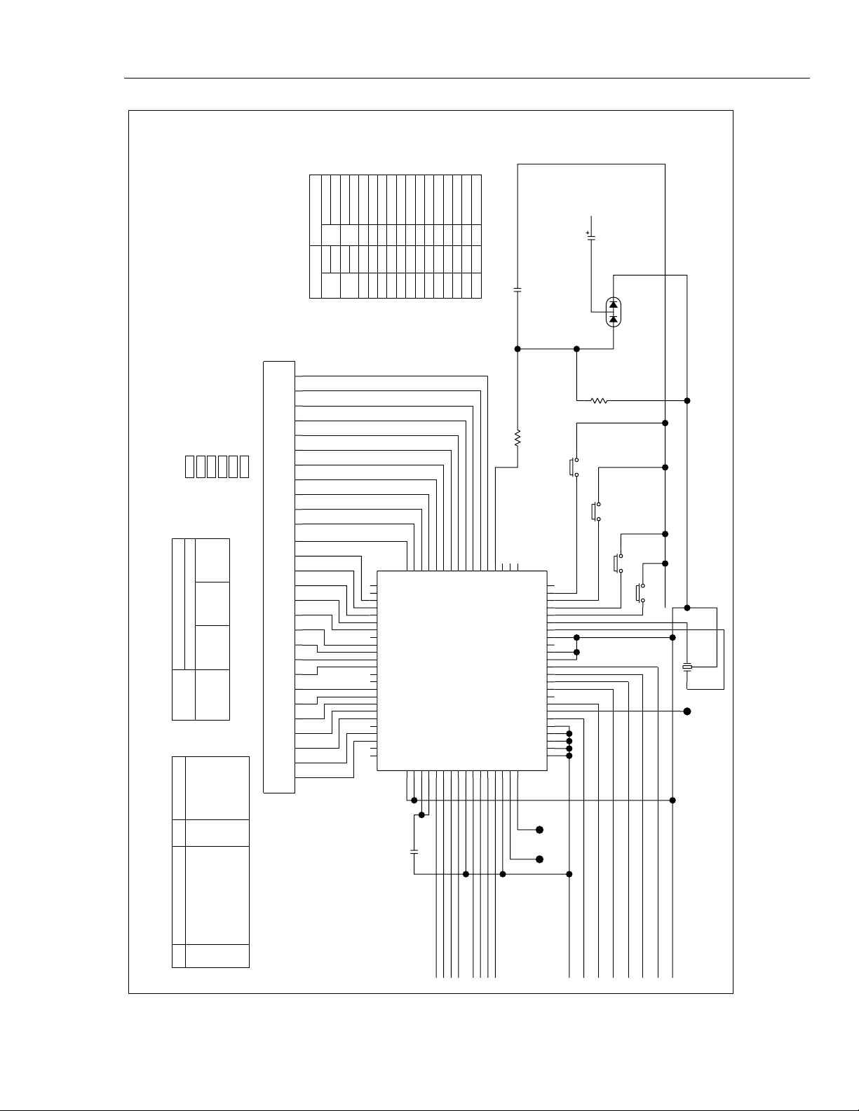
Parts and Schematics
Parts Lists, Drawings, and Schematics
20
11, 12
C
16
30
REFERENCE DESIGNATION
+/ - 1 0 %, CERAMI C.
+/ - 5%, CERMET. +/ - 1% RESI STORS ARE 1/ 8 WATT,
CERMET.4.R19 I S A FUSI BL E RESI STOR. EXACT
REPLACEMENT ONLY.
C4, 9, 12 & 1 3 MAY HAVE +/ - 20% TOLERANCE.
1.
2. ALL CAPACI TANCE VALUES ARE I N MI CROFARADS,
NOTES: UNLESS OTHERWI SE SPECI FI ED:
SELECT
S2
1
MEMBRANE T AIL
PI N ASSIGNMENTS
5
3. AL L RESI STANCE VALUES ARE I N OHMS, 1/ 8 WATT,
RANGE
2
6. R11 AND R12 MAY HAVE +/ - 0. 25 % TOLERANCE.
7. R23 MAY HAVE +/ - 5% TOLERANCE.
8.
26252423222120191817161514131211109876543 282 271
APACI TANCE
VSS
VSSCMIN/MAX
654
3
CRU
LAST USED NOT USED
1
322
2
8
311
111
1
10%
J
BT
CR
LS
Q
S
TP
RT
YZVR
E
0. 1
C13
25V
1%
R23
1. 0M
VDD
C10
S2
MI N / MAX
45
AL
20%
22
10V
CR3
BAV99
2. 2M
R25
S2
35
CAPACI TANCE
(2 of 2)
FLUKE 7-600-1201
4
S1 C ONNECT I VI TY TABL E
COMPONENT TYPE ABBREVIATION CODES
OPEN
4- 52- 31- 2
OPEN
CONTACTS
OPEN
OF F
POSITI ON
MET A L GL AZ E
WI RE WOUND
MGWWMF
MYLAR/ POLYESTER
CERAMIC
MCTPCPP
SYM CAPACITOR SYM RESI STOR
OPEN
OPEN
CLOSED
HIGH Z
METAL FILM
TANTAL UM
CLOSED
CLOSED
CLOSED
LOW Z
CARBON COMPCC
POLY CARBONATE
78777675747372
80
U3
12345678910111213141516171819202122232425262728
CARBON FI LMCF
AL UMINUMAL
POLYPROPYLENE FILM
79
S9
S12
S11
S10
1
S13
2
S14
3
S15
4
S16
5
S17
6
S18
7
S19
8
S20
9
S21
10
S22
11
S23
12
S24
13
S25
14
S26
15
S27
16
S28
17
S29
18
S30
19
S31
20
COM0
21
COM1
22
COM2
23
COM3
24
BI AS
25
10%
C4
VLC1
VLC0
282726
25V
0. 1
VLC2
29
ADR0
P40
ADR1
P41
ADR2
P42
323130
ADR3
71
U2
VSS
P43
33
34
ADR4
706966
68
67
S0S1S2S3S4S5S6S7S8
RESET*
P53
P52
P51
P50
373635
38
WRI TE*
READ*
ADR5
65
P70
P71
P72
P73
SCK
P00
39
64
P63
63
P62
62
P61
61
P60
60
X2
59
X1
58
VPP
57
XT2
56
XT1
55
VDD
54
P33
53
P32
52
P31
51
P30
50
P23
49
P22
48
P21
47
P20
46
P13
45
P12
44
P11
43
P10
42
P03
41
SO
40
S2
RANGE
25
S2
15
VSS2
SELECT
.5%
Y1
TP3 2. 1MHZ
AZEND
SOUTSCLK
TP2 TP1
DATA0
DATA1
DATA2
VSS1
CLK
BCLK
DATA3
DGND
Figure 4-7. Model 7-600 Schematic (cont)
as19f.eps
4-17
Page 51

12B/18/7 Series
Service Manual
4-18
Page 52

Service Centers
PN 850941 2/96
Page 53

Service Centers (cont)
2/96
 Loading...