


FLC-BTM403 Series User Manual
FLC-BTM403 Series
User Manual
Document Type: Bluetooth Module User Manual
Document Number: FLC-BTM403-DS
Document Version: V1.0
Release Date: April 13, 2011
Copyright 2010 ~ 2011 by Flaircomm Technologies Inc., All Right Reserved
Without written permission from Flaircomm Technologies Inc., reproduction, transfer, distribution or
storage of part or all of the contents in this document in any form is prohibited
Flaircomm Technologies Confidential
-1-

FLC-BTM403 Series User Manual
FCC Regulations:
zThis device complies with part 15 of the FCC Rules. Operation is subject to the following two conditions: (1) This
device may not cause harmful interference, and (2) this device must accept any interference received, including
interference that may cause undesired operation.
zThis device has been tested and found to comply with the limits for a Class B digital device, pursuant to Part 15 of the
FCC Rules. These limits are designed to provide reasonable protection against harmful interference in a residential
installation. This equipment generates, uses and can radiated radio frequency energy and, if not installed and used in
accordance with the instructions, may cause harmful interference to radio communications. However, there is no
guarantee that interference will not occur in a particular installation If this equipment does cause harmful interference to
radio or television reception, which can be determined by turning the equipment off and on, the user is encouraged to try
to correct the interference by one or more of the following measures:
-Reorient or relocate the receiving antenna.
-Increase the separation between the equipment and receiver.
-Connect the equipment into an outlet on a circuit different from that to which the receiver is connected.
-Consult the dealer or an experienced radio/TV technician for help.
Changes or modifications not expressly approved by the party responsible for compliance could void the user‘s authority
to operate the equipment.
4RF Exposure Information
This Modular Approval is limited to OEM installation for mobile and fixed applications only. The antenna installation
and operating configurations of this transmitter, including any applicable source-based time-averaging duty factor,
antenna gain and cable loss must satisfy MPE categorical Exclusion Requirements of §2.1091.
The end user has no manual instructions to remove or install the device and a separate approval is required for all other
operating configurations, including portable configurations with respect to 2.1093 and different antenna configurations.
Maximum antenna gain allowed for use with this device is 0.5 dBi.
When the module is installed in the host device, the FCC ID label must be visible through a window on the final device
or it must be visible when an access panel, door or cover is easily re-moved. If not, a second label must be placed on the
outside of the final device that contains the following text: “Contains FCC ID: TQ6BTM403”.
Flaircomm Technologies Confidential
-2-

FLC-BTM403 Series User Manual
CONTENT
1. INTRODUCTION.................................................................................................................................5
1.1 NAMING DECLARATION .......................................................................................................................5
1.2 FEATURES ............................................................................................................................................5
1.3 APPLICATIONS ..................................................................................................................................... 6
2. GENERAL SPECIFICATION ............................................................................................................7
3. PIN DEFINITION.................................................................................................................................8
3.1 PIN CONFIGURATION............................................................................................................................8
3.2 PIN DEFINITION....................................................................................................................................8
4. PHYSICAL INTERFACES ...............................................................................................................10
4.1 POWER SUPPLY ..................................................................................................................................10
4.2 RESET ................................................................................................................................................ 10
4.3 DIGITAL AUDIO INTERFACES ............................................................................................................. 11
4.3.1 PCM Interface Master/Slave .....................................................................................................11
4.3.2 Long Frame Sync ......................................................................................................................12
4.3.3 Short Frame Sync ...................................................................................................................... 13
4.3.4 Multi-slot Operation .................................................................................................................. 13
4.3.5 GCI Interface............................................................................................................................. 14
4.3.6 Slots and Sample Formats .........................................................................................................14
4.3.7 Additional Features ...................................................................................................................15
4.3.8 PCM Timing Information..........................................................................................................15
4.4 RF INTERFACE ...................................................................................................................................19
4.5 GENERAL PURPOSE ANALOGUE IO ....................................................................................................19
4.6 GENERAL PURPOSE DIGITAL IO......................................................................................................... 19
4.7 SERIAL INTERFACES ........................................................................................................................... 19
4.7.1 UART........................................................................................................................................ 19
4.7.2 USB........................................................................................................................................... 20
4.7.3 I2C .............................................................................................................................................22
4.7.4 SPI............................................................................................................................................. 22
5. ELECTRICAL CHARACTERISTIC...............................................................................................24
5.1 ABSOLUTE MAXIMUM RATING ..........................................................................................................24
5.2 RECOMMEND OPERATION CONDITIONS ..............................................................................................24
5.3 POWER CONSUMPTIONS...................................................................................................................... 24
5.4 INPUT/OUTPUT TERMINAL CHARACTERISTICS ................................................................................... 24
5.4.1 Digital Terminals....................................................................................................................... 24
5.4.2 USB........................................................................................................................................... 25
6. REFERENCE DESIGN......................................................................................................................26
7. MECHANICAL CHARACTERISTIC .............................................................................................27
8. RECOMMENDED PCB LAYOUT AND MOUNTING PATTERN..............................................28
9. RECOMMENDED REFLOW PROFILE........................................................................................29
10. ORDERING INFORMATION......................................................................................................30
10.1 PRODUCT PACKAGING INFORMATION ................................................................................................30
10.2 ORDERING INFORMATION................................................................................................................... 31
10.2.1 Product Revision .......................................................................................................................31
10.2.2 Shipping Package ......................................................................................................................31
10.2.3 Product Package ........................................................................................................................31
10.2.4 Product Grade............................................................................................................................31
Flaircomm Technologies Confidential
-3-

FLC-BTM403 Series User Manual
TABLE AND FIGURE
Table 1: Naming Declaration.......................................................................................................................... 5
Table 2: General Specification........................................................................................................................ 7
Table 3: Pin Definition.................................................................................................................................... 9
Table 4: Pin Status on Reset..........................................................................................................................11
Table 5: PCM Master Timing .......................................................................................................................16
Table 6: PCM Slave Timing..........................................................................................................................18
Table 7: Possible UART Settings..................................................................................................................20
Table 8: USB Interface Component Values .................................................................................................. 21
Table 9: Absolute Maximum Rating Recommended Operating Conditions................................................. 24
Table 10: Recommended Operating Conditions ........................................................................................... 24
Table 11: Power consumptions ..................................................................................................................... 24
Table 12: Digital Terminal............................................................................................................................ 25
Table 13: USB Terminal ...............................................................................................................................25
Table 14: Product Revision...........................................................................................................................31
Table 15: Shipping Package.......................................................................................................................... 31
Table 16: Product Package............................................................................................................................ 31
Table 17: Product Grade ...............................................................................................................................32
Figure 1: Pin Configuration.............................................................................................................................8
Figure 2: Configured PCM as a Master.........................................................................................................12
Figure 3: Configured PCM as a Slave........................................................................................................... 12
Figure 4: Long Frame Sync (Shown with 8-bit Companded Sample) ..........................................................13
Figure 5: Short Frame Sync (Shown with 16-bit Sample) ............................................................................13
Figure 6: Multi-Slot Operation with Two Slots and 8-bit Companded Samples........................................... 14
Figure 7: GCI Interface .................................................................................................................................14
Figure 8: 16-Bit Slot Length and Sample Formats........................................................................................ 15
Figure 9: PCM Master Timing Long Frame Sync.........................................................................................17
Figure 10: PCM Master Timing Short Frame Sync ......................................................................................17
Figure 11: PCM Slave Timing Long Frame Sync......................................................................................... 18
Figure 12: PCM Master Timing Short Frame Sync ......................................................................................19
Figure 13: USB Connections for Self-Powered Mode ..................................................................................21
Figure 14: USB Connections for Bus-Powered Mode ..................................................................................22
Figure 15: Example EEPROM Connection with I2C Interface ..................................................................... 22
Figure 16: Design SPI for In-System Programming and Debug ...................................................................23
Figure 17: Reference Design......................................................................................................................... 26
Figure 18: Mechanical Characteristic............................................................................................................27
Figure 19: Leave 20mm Clearance Space from the Module chip Antenna................................................... 28
Figure 20: Recommended Reflow Profile..................................................................................................... 29
Figure 21: Product Packaging Information ...................................................................................................31
Figure 22: Ordering Information................................................................................................................... 31
Flaircomm Technologies Confidential
-4-
FLC-BTM403 Series User Manual
1. Introduction
FLC-BTM403/FLC-BTMDC748 is a small form factor and highly economic Bluetooth radio
module(class 1 or class 2) that allows OEM to add wireless capability to their products. The module
supports multiple interfaces that make it simple to design into fully certified embedded Bluetooth
solutions.
With FLC’s AT#™ programming interfaces, designers can easily customize their applications to
support different Bluetooth profiles, such as SPP, DUN, HDP, and etc. class1 module supports
Bluetooth® Enhanced Data Rate (EDR) and delivers up to 3 Mbps data rate for distances up to 300
meters with its integrated chip antenna, class 2 module supports 3Mbps data rate Transmission for
distances up to 10 meters with its integrated chip antenna.
The module is an appropriate product for designers who want to add wireless capability to their
products.
Note: According to the software divided into class1 and class2
1.1 Naming Declaration
New Naming Old Naming
FLC-BTM403A FLC-BTMDC748A(class1)
FLC-BTM403B FLC-BTMDC748B(class1)
FLC-BTM403C FLC-BTMDC748C(class2)
Table 1: Naming Declaration
1.2 Features
z Bluetooth v2.1+EDR
z UART and USB programming and data interfaces
z PCM digital audio interfaces
z 8MB on board flash
z Small form factor
z SMT pads for easy and reliable PCB mounting
z BQB/FCC/CE Certified
z RoHS compliant
Flaircomm Technologies Confidential
-5-

FLC-BTM403 Series User Manual
1.3 Applications
z Cable replacement
z Bar code and RFID scanners
z Measurement and monitoring systems
z Industrial sensors and controls
z Medical devices
z Industrial PCs and laptops
Flaircomm Technologies Confidential
-6-
FLC-BTM403 Series User Manual
2. General Specification
Bluetooth Specification
Standard Bluetooth2.1+EDR
Profiles
Frequency Band 2.402G ~ 2.480G
Maximum Data Rate 3Mbps
Antenna Multilayer Ceramic Antenna or UFL port
RF Input Impedance 50 ohms
Baseband Crystal OSC 16MHz
Interface UART, PIO, AIO, USB, SPI, PCM
Sensitivity -84dBm@0.1%BER
RF TX Power +13dBm(class1) +4dbm(class2)
detailed profiles depends on the firmware
SPP, DUN, HDP,
Power
Supply Voltage 3 ~ 3.6V DC
Working Current Depends on profiles, 22mA typical
Standby Current(Connected) <2mA
Operating Environment
Temperature -20ºC to +55ºC
Humidity 10%~90% Non-Condensing
Certifications
Environmental
BQB/FCC/CE
RoHS Compliant
Dimension and Weight
Dimension 35.30mm×14.00mm×2.50mm
Weight 2.00g
Table 2: General Specification
Flaircomm Technologies Confidential
-7-
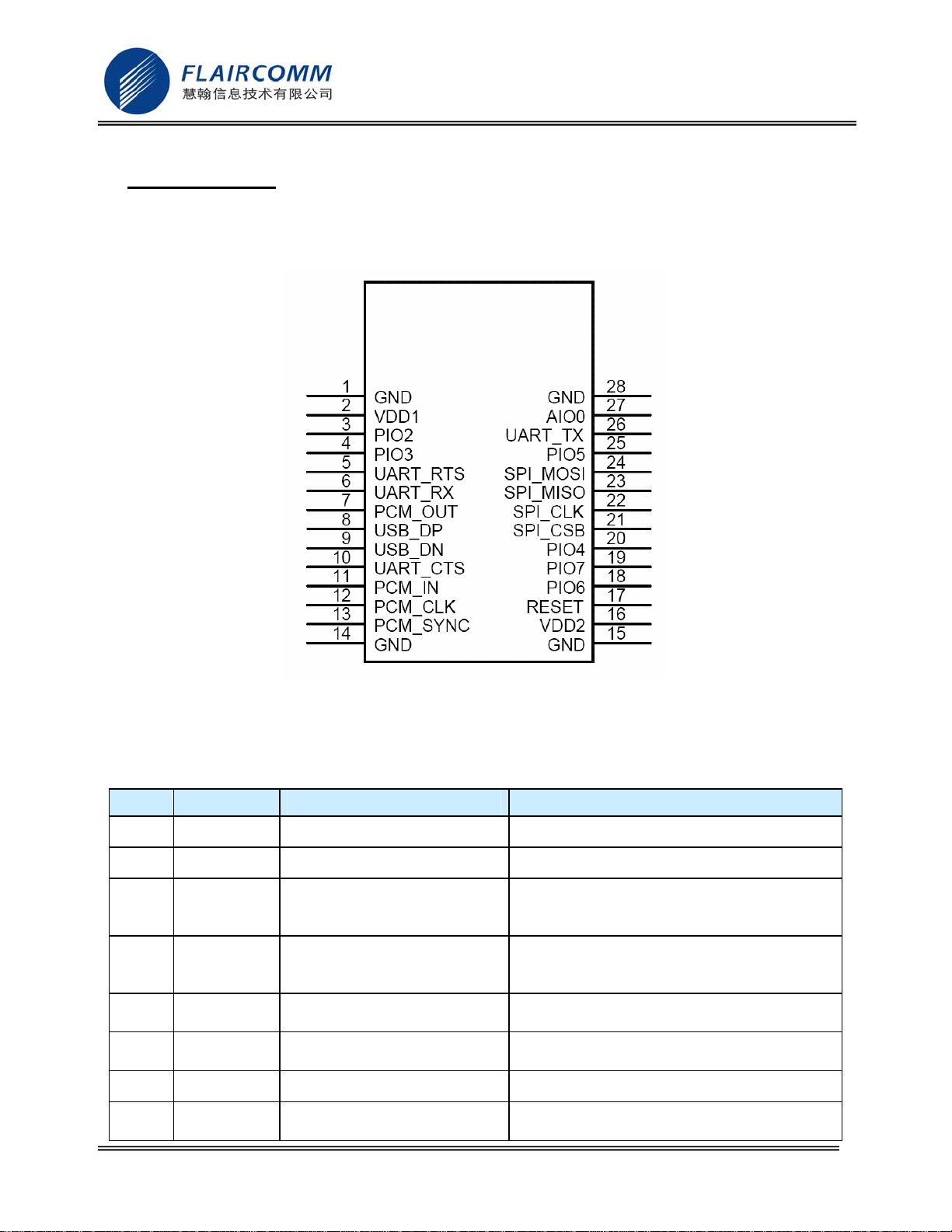
3. Pin Definition
3.1 Pin Configuration
FLC-BTM403 Series User Manual
Figure 1: Pin Configuration
3.2 Pin Definition
Pin Symbol I/O Type Description
1 GND Ground Ground
2 VDD 3V3 power input 3V3 power input
Bi-directional with
3 PIO2
4 PIO3
5 UART_RTS
6 UART_RX
7 PCM_OUT Bi-directional Synchronous Data Output
8 USB_DP Bi-directional
programmable strength internal
pull-up/down
Bi-directional with
programmable strength internal
pull-up/down
CMOS output, tri-state, with
weak internal pull-up
CMOS input with weak internal
pull-down
USB data plus with selectable internal 1.5Kohm
Programmable input/output line
Programmable input/output line
UART request to send active low
UART data input
pull-up resistor
Flaircomm Technologies Confidential
-8-

FLC-BTM403 Series User Manual
9 USB_DN Bi-directional USB data minus
10 UART_CTS
CMOS output, tri-state, with
weak internal pull-down
UART clear to send active low
11 PCM_IN CMOS Input Synchronous Data Input
12 PCM_CLK Bi-directional Synchronous Data Clock
13 PCM_SYNC Bi-directional Synchronous Data Sync
14 GND Ground Ground
15 GND Ground Ground
16 VDD 3.3V power input 3.3V power input
17 RESET
CMOS input with weak internal
pull-down
Reset if high. Input debounced so must be high
for >5ms to cause a reset
Bi-directional with
18 PIO6
programmable strength internal
Programmable input/output line
pull-up/down
Bi-directional with
19 PIO7
programmable strength internal
Programmable input/output line
pull-up/down
Bi-directional with
20 PIO4
programmable strength internal
Programmable input/output line
pull-up/down
21 SPI_CSB
CMOS input with weak internal
22 SPI_CLK
23 SPI_MISO
24 SPI_MOSI
pull-up
input with weak internal pull-
down
CMOS output, tri-state, with
weak internal pull-down
CMOS input, with weak
internal pull-down
Chip select for Synchronous Serial Interface
active low
Serial Peripheral Interface clock
Serial Peripheral Interface output
Serial Peripheral Interface input
Bi-directional with
25 PIO5
programmable strength internal
Programmable input/output line
pull-up/down
26 UART_TX
CMOS input with weak internal
pull-down
UART data output
27 AIO0 Bi-directional Programmable input/output line
28 GND Ground Ground
Table 3: Pin Definition
Flaircomm Technologies Confidential
-9-
FLC-BTM403 Series User Manual
4. Physical Interfaces
4.1 Power Supply
The transient response of the regulator is important. If the power rails of the module are supplied
from an external voltage source, the transient response of any regulator used should be 20μs or less.
It is essential that the power rail recovers quickly.
4.2 Reset
The module may be reset from several sources: RESET pin, power-on reset, a UART break
character or via a software configured watchdog timer.
The RESET pin is an active high reset and is internally filtered using the internal low frequency
clock oscillator. A reset will be performed between 1.5 and 4.0ms following RESET being active. It
is recommended that RESET be applied for a period greater than 5ms.
The module has an internal reset circuitry, which keeps reset pin active until supply voltage has
reached stability in the start up. This ensures that supply for the flash memory inside the module will
reach stability before BC4 chip fetches instructions from it. Pull-up or pull-down
not be connected to the reset pin to ensure proper star up of
module
.
resistor
should
At reset the digital I/O pins are set to inputs for bi-directional pins and outputs are tri-state. The PIOs
have weak pull-downs.
Pin Name / Group Pin Status on Reset
USB_DP Input with PD
USB_DN Input with PD
UART_RX Input with PD
UART_CTS Input with PD
UART_TX Tri-state output with PU
UART_RTS Tri-state output with PU
SPI_MOSI Input with PD
SPI_CLK Input with PD
SPI_CSB Input with PU
SPI_MISO Tri-state output with PD
PCM_CLK Input with PD
PCM_SYNC Input with PD
PCM_IN Input with PD
PCM_OUT Tri-state with PD
RESETB Input with PU
PIOs Input with weak PD
AIOs Output, driving low
Flaircomm Technologies Confidential
-10-

FLC-BTM403 Series User Manual
RF-IN High impedance
Table 4: Pin Status on Reset
Note: Pull-up (PU) and pull-down (PD) default to weak values unless specified otherwise.
4.3 Digital Audio Interfaces
The module has offered PCM digital audio interface.
PCM is a standard method used to digitize audio (particularly voice) for transmission over digital
communication channels. Through its PCM interface, the module has hardware support for continual
transmission and reception of PCM data, thus reducing processor overhead for applications. The
module offers a bi-directional digital audio interface that routes directly into the baseband layer of
the on-chip firmware. It does not pass through the HCI protocol layer.
Hardware on the module allows the data to be sent to and received from a SCO connection. Up to
three SCO connections can be supported by the PCM interface at any one time.
The module can operate as the PCM interface master generating an output clock of 128, 256 or
512kHz. When configured as PCM interface slave, it can operate with an input clock up to 2048kHz.
The module is compatible with a variety of clock formats, including Long Frame Sync, Short Frame
Sync and GCI timing environments.
It supports 13-bit or 16-bit linear, 8-bit µ-law or A-law companded sample formats at 8k samples/s
and can receive and transmit on any selection of three of the first four slots following PCM_SYNC.
The module interfaces directly to PCM audio devices including the following:
z Qualcomm MSM 3000 series and MSM 5000 series CDMA baseband devices
z OKI MSM7705 four channels A-law and µ-law CODEC
z Motorola MC145481 8 -bit A-law and µ-law CODEC
z Motorola MC145483 13 -bit linear CODEC
z STW 5093 and 5094 14 -bit linear CODECs
The module is also compatible with the Motorola SSI™ interface.
4.3.1 PCM Interface Master/Slave
When PCM is configured as a master, the module generates PCM_CLK and PCM_SYNC.
Flaircomm Technologies Confidential
-11-

FLC-BTM403 Series User Manual
Figure 2: Configured PCM as a Master
When PCM is configured as the slave, the module accepts PCM_CLK rates up to 2048kHz.
Figure 3: Configured PCM as a Slave
4.3.2 Long Frame Sync
Long Frame Sync is the name given to a clocking format that controls the transfer of PCM data
words or samples. In Long Frame Sync, the rising edge of PCM_SYNC indicates the start of the
PCM word. When the module is configured as PCM master, generating PCM_SYNC and
PCM_CLK, then PCM_SYNC is 8-bits long. When the module is configured as PCM Slave,
PCM_SYNC may be from two consecutive falling edges of PCM_CLK to half the PCM_SYNC rate,
i.e., 62.5µs long.
Flaircomm Technologies Confidential
-12-

FLC-BTM403 Series User Manual
Figure 4: Long Frame Sync (Shown with 8-bit Companded Sample)
4.3.3 Short Frame Sync
In Short Frame Sync, the falling edge of PCM_SYNC indicates the start of the PCM word.
PCM_SYNC is always one clock cycle long.
Figure 5: Short Frame Sync (Shown with 16-bit Sample)
As with Long Frame Sync, the module samples PCM_IN on the falling edge of PCM_CLK and
transmits PCM_OUT on the rising edge. PCM_OUT may be configured to be high impedance on the
falling edge of PCM_CLK in the LSB position or on the rising edge.
4.3.4 Multi-slot Operation
More than one SCO connection over the PCM interface is supported using multiple slots. Up to three
SCO connections can be carried over any of the first four slots.
Flaircomm Technologies Confidential
-13-

FLC-BTM403 Series User Manual
Figure 6: Multi-Slot Operation with Two Slots and 8-bit Companded Samples
4.3.5 GCI Interface
The module is compatible with the General Circuit Interface (GCI), a standard synchronous 2B+D
ISDN timing interface. The two 64Kbps B channels can be accessed when this mode is configured.
Figure 7: GCI Interface
The start of a frame is indicated by the rising edge of PCM_SYNC and runs at 8kHz. With the
module in slave mode, the frequency of PCM_CLK can be up to 4.096MHz.
4.3.6 Slots and Sample Formats
The module can receive and transmit on any selection of the first four slots following each sync
pulse. Slot durations can be either 8 or 16 clock cycles. Durations of 8 clock cycles may only be
used with 8-bit sample formats. Durations of 16 clocks may be used with 8-bit, 13-bit or 16-bit
sample formats. The module supports 13-bit linear, 16-bit linear and 8-bit µ-law or A-law sample
formats. The sample rate is 8k samples/s. The bit order may be little or big endian. When 16-bit slots
are used, the 3 or 8 unused bits in each slot may be filled with sign extension, padded with zeros or a
programmable 3-bit audio attenuation compatible with some Motorola CODECs.
Flaircomm Technologies Confidential
-14-

FLC-BTM403 Series User Manual
Figure 8: 16-Bit Slot Length and Sample Formats
4.3.7 Additional Features
The module has a mute facility that forces PCM_OUT to be 0. In master mode, PCM_SYNC may
also be forced to 0 while keeping PCM_CLK running which some CODECS use to control power
down.
4.3.8 PCM Timing Information
Symbol Parameter Min Typical Max Unit
fmclk
PCL_CLK
Frequency
4MHz DDS generation.
Selection of frequency
is programmable.
128
-
256
512
- kHz
Flaircomm Technologies Confidential
-15-

- PCM_SYNC frequency - 8 kHz
tmclkh
tmclkl
-
tdmclksynch
tdmclkpout
tdmclklsyncl
tdmclkhsyncl
tdmclklpoutz
tdmclkhpoutz
tsupinclkl
thpinclkl
FLC-BTM403 Series User Manual
48MHz DDS
generation. Selection of
frequency is
2.9 - kHz
programmable.
(a)
(a)
PCM_CLK
high
4MHz DDS generation 980 - - ns
PCM_CLK low 4MHz DDS generation 730 - ns
PCM_CLK
jitter
Delay time from PCM_CLK high to
PCM_SYNC high
Delay time from PCM_CLK high to valid
PCM_OUT
Delay time from PCM_CLK low to
PCM_SYNC low (Long Frame Sync only)
Delay time from PCM_CLK high to
PCM_SYNC low
Delay time from PCM_CLK low to
PCM_OUT high impedance
Delay time from PCM_CLK high to
PCM_OUT high impedance
Set-up time for PCM_IN valid to
PCM_CLK low
Hold time for PCM_CLK low to PCM_IN
invalid
48MHz DDS
generation
21 ns pk-pk
- - 20 ns
- - 20 ns
- - 20 ns
- - 20 ns
- - 20 ns
- - 20 ns
30 - - ns
10 - - ns
Table 5: PCM Master Timing
Flaircomm Technologies Confidential
-16-

FLC-BTM403 Series User Manual
Figure 9: PCM Master Timing Long Frame Sync
Figure 10: PCM Master Timing Short Frame Sync
Symbol Parameter Min Typical Max Unit
fsclk PCM clock frequency (Slave mode: input) 64 - 2048 kHz
fsclk PCM clock frequency (GCI mode) 128 - 4096 kHz
Flaircomm Technologies Confidential
-17-

thsclksynch
tsusclksynch
tdsclkhpout
tsupinsclkl
thpinsclkl
FLC-BTM403 Series User Manual
tsclkl PCM_CLK low time 200 - - ns
tsclkh PCM_CLK high time 200 - - ns
tdpout
tdpoutz
Hold time from PCM_CLK low to
PCM_SYNC high
Set-up time for PCM_SYNC high to
PCM_CLK low
Delay time from PCM_SYNC or
PCM_CLK whichever is later, to valid
PCM_OUT data (Long Frame Sync only)
Delay time from CLK high to PCM_OUT
valid data
Delay time from PCM_SYNC or
PCM_CLK low, whichever is later, to
PCM_OUT data line high impedance
Set-up time for PCM_IN valid to CLK
low
Hold time for PCM_CLK low to
PCM_IN invalid
Table 6: PCM Slave Timing
30 - - ns
30 - - ns
- -
- -
- -
20
20
20
ns
ns
ns
30 - - ns
30 - - ns
Figure 11: PCM Slave Timing Long Frame Sync
Flaircomm Technologies Confidential
-18-

FLC-BTM403 Series User Manual
Figure 12: PCM Master Timing Short Frame Sync
4.4 RF Interface
The module integrates a balun filter. The user can connect a 50ohms antenna directly to the RF port.
4.5 General Purpose Analogue IO
The general purpose analogue IO can be configured as ADC inputs by software. Do not connect
them if not use.
4.6 General Purpose Digital IO
The general purpose digital IO can be configured by software to have various functions such as
button, LED or interrupt signals to host controller. Do not connect them if not use.
4.7 Serial Interfaces
4.7.1 UART
This is a standard Universal Asynchronous Receiver Transmitter (UART) interface for
communicating with other serial devices. Four signals UART_TX, UART_RX, UART_CTS, and
UART_RTS are used to implement the UART function, UART_CTS, UART_RTS can be used to
implement hardware flow control. PIO2 and PIO3 can be configured as DTR and RTS.
Flaircomm Technologies Confidential
-19-

FLC-BTM403 Series User Manual
Parameter Possible Values
Baud Rate Minimum
Maximum 3M baud (≤1%Error)
Flow Control RTS/CTS or None
Parity None, Odd or Even
Number of Stop Bits 1 or 2
Bits per Byte 8
Table 7: Possible UART Settings
1200 baud (≤2%Error)
9600 baud (≤1%Error)
4.7.2 USB
There is a full speed (12M bits/s) USB interface for communicating with other compatible digital
devices. The module acts as a USB peripheral, responding to request from a master host controller,
such as a PC.
The module features an internal USB pull-up resistor. This pulls the USB_DP pin weakly high when
module is ready to enumerate. It signals to the USB master that it is a full speed (12Mbit/s) USB
device. The USB internal pull-up is implemented as a current source, and is compliant with section
7.1.5 of the USB specification v1.2. The internal pull-up pulls USB_DP high to at least 2.8V when
loaded with a 15kΩ ±5% pull-down resistor (in the hub/host) when VDD =3.1V. This presents a
Thevenin resistance to the host of at least 900Ω. Alternatively, an external 1.5kΩ pull-up resistor can
be placed between a PIO line and DP on the USB cable.
4.7.2.1 Self-Powered Mode
In self-powered mode, the module is powered from its own power supply and not from the VBUS
(5V) line of the USB cable. It draws only a small leakage current (below 0.5mA) from VBUS on the
USB cable. This is the easier mode for which to design, as the design is not limited by the power that
can be drawn from the USB hub or root port. However, it requires that VBUS be connected to
module via a resistor network (Rvb1 and Rvb2), so the module can detect when VBUS is powered
up. The module will not pull USB_DP high when VBUS is off.
Self-powered USB designs (powered from a battery or LDO) must ensure that a PIO line is allocated
for USB pull-up purposes. A 1.5KΩ 5% pull-up resistor between USB_DP and the selected PIO line
should be fitted to the design. Failure to fit this resistor may result in the design failing to be USB
compliant in self-powered mode. The internal pull-up in the module is only suitable for bus-powered
USB devices, e.g., dongles.
Flaircomm Technologies Confidential
-20-

Note:
FLC-BTM403 Series User Manual
Figure 13: USB Connections for Self-Powered Mode
USB_ON is shared with the module PIO terminals.
Identifier Value Function
R
s
Rvb1 22kΩ 5% VBUS ON sense divider
Rvb2 47kΩ 5% VBUS ON sense divider
Table 8: USB Interface Component Values
27Ω Nominal Impedance matching to USB cable
4.7.2.2 Bus-Powered Mode
In bus-powered mode, the application circuit draws its current from the 5V VBUS supply on the
USB cable. The module negotiates with the PC during the USB enumeration stage about how much
current it is allowed to consume. For Class 2 Bluetooth applications, FLC recommends that the
regulator used to derive 3.3V from VBUS is rated at 100mA average current and should be able to
handle peaks of 120mA without foldback or limiting. In bus-powered mode, the module requests
100mA during enumeration. For Class 1 Bluetooth applications, the USB power descriptor should be
altered to reflect the amount of power required. This is higher than for a Class 2 application due to
the extra current drawn by the Transmit RF PA. When selecting a regulator, be aware that VBUS
may go as low as 4.4V. The inrush current (when charging reservoir and supply decoupling
capacitors) is limited by the USB specification. See USB Specification v1.1, section 7.2.4.1. Some
applications may require soft start circuitry to limit inrush current if more than 10µF is present
between VBUS and GND.
Flaircomm Technologies Confidential
-21-

4.7.3 I2C
FLC-BTM403 Series User Manual
Figure 14: USB Connections for Bus-Powered Mode
PIO5, PIO7 and PIO6 can be used to form a master I2C interface. The interface is formed using
software to drive these lines. It is suited only to relatively slow functions such as driving a LCD,
Keyboard, scanner or EEPROM. In the case, PIO lines need to be pulled up through 2.2Kohm
resistors.
Figure 15: Example EEPROM Connection with I
2
C Interface
4.7.4 SPI
he synchronous serial port interface (SPI) can be used for system debugging. It can also be used for
in-system programming for the flash memory within the module. SPI interface uses the SPI_MOSI,
SPI_MISO, SPI_CSB and SPI_CLK pins. Testing points for the SPI interface are reserved on board
in case that the firmware shall be updated during manufacture.
The module operates as a slave and thus SPI_MISO is an output of the module. SPI_MISO is not in
high-impedance state when SPI_CSB is pulled high. Instead, the module outputs 0 if the processor is
running and 1 if it is stopped. Thus the module should NOT be connected in a multi-slave
Flaircomm Technologies Confidential
-22-

FLC-BTM403 Series User Manual
arrangement by simple parallel connection of slave SPI_MISO lines. The SPI interface is needed
when debugging the Bluetooth functions so please leave test points/pads as shown in Figure 16 on
PCB.
VDD
PC
The Module
SPI-CSB
SPI-MISO
SPI-MOSI
SPI-CLK
GND
System
Mainboard
Download Cable &
Adaptor by Flaircomm
Pad or
Connector
Figure 16: Design SPI for In-System Programming and Debug
Flaircomm Technologies Confidential
-23-

FLC-BTM403 Series User Manual
5. Electrical Characteristic
5.1 Absolute Maximum Rating
Rating Min Max Unit
Storage Temperature -40 +120 °C
Operating Temperature -40 +85 °C
PIO/AIO Voltage -0.4 +3.6 V
VDD Voltage -0.4 +3.7 V
USB_DP/USB_DN Voltage -0.4 +3.6 V
Other Terminal Voltages except RF -0.4 VDD+0.4 V
Table 9: Absolute Maximum Rating Recommended Operating Conditions
5.2 Recommend operation conditions
Operating Condition Min Typical Max Unit
Storage Temperature -40 -- +85 °C
Operating Temperature Range -20 -- +70 °C
VDD Voltage +3 +3.3 +3.6 V
Table 10: Recommended Operating Conditions
5.3 Power consumptions
Operating Condition Min Typical Max Unit
Radio On*(Discovery)
Radio On*( Inquiry window time)
Connected Idle (No Sniff)
Connected with data transfer
Table 11: Power consumptions
*If in SLAVE mode there are bursts of radio ON time which vary with the windows. Depending on how you set the
windows that determines your average current.
23 mA
73 mA
20 mA
6 10 25 mA
5.4 Input/output Terminal Characteristics
5.4.1 Digital Terminals
Supply Voltage Levels Min Typical Max Unit
Input Voltage Levels
Flaircomm Technologies Confidential
-24-

FLC-BTM403 Series User Manual
V
input logic level low -0.4
IL
-
+0.8 V
VIH input logic level high 0.7VDD - VDD+0.4 V
Output Voltage Levels
VOL output logic level low, lOL = 4.0mA - - 0.4 V
VOH output logic level high, lOH = -4.0mA VDD-0.2 - - V
Input and Tri-state Current
With strong pull-up -100 -40 -10 μA
With strong pull-down 10 40 100 μA
With weak pull-up -5 -1.0 -0.2 μA
With weak pull-down -0.2 +1.0 5.0 μA
I/O pad leakage current -1 0 +1 μA
CI Input Capacitance 1.0 - 5.0 pF
Table 12: Digital Terminal
5.4.2 USB
USB Terminals Min Typical Max Unit
Input Threshold
VIL input logic level low - - 0.3VDD V
VIH input logic level high 0.7VDD - - V
Input Leakage Current
GND < VIN < VDD
CI Input capacitance 2.5 - 10.0 pF
Output Voltage Levels to Correctly Terminated USB Cable
V
output logic level low 0.0 - 0.2 V
IL
VIH output logic level high 2.8 - VDD V
(a)
-1 1 5 μA
Table 13: USB Terminal
(a) Internal USB pull-up disabled
Flaircomm Technologies Confidential
-25-

6. Reference Design
FLC-BTM403 Series User Manual
Figure 17: Reference Design
Flaircomm Technologies Confidential
-26-

FLC-BTM403 Series User Manual
7. Mechanical Characteristic
Figure 18: Mechanical Characteristic
Flaircomm Technologies Confidential
-27-

FLC-BTM403 Series User Manual
8. Recommended PCB Layout and Mounting Pattern
A very important factor in achieving maximum Bluetooth performance is the placement of a module
with on-board antenna designs onto the carrier board and corresponding PCB layout. There should
be no any trace, ground and vias in the area of the carrier board underneath the module’s on-board
antenna section as indicated in Figure 19. Antenna portion of the module must be placed at least
20mm away from any metal part and the antenna should not be covered by any piece of metal. The
antenna of the module MUST be kept as far from potential noise sources as possible and special care
must also be taken with placing the module in proximity to circuitry that can emit heat. The RF part
of the module is very sensitive to temperature and sudden changes can have an adverse impact on
performance.
Figure 19: Leave 20mm Clearance Space from the Module chip Antenna
Flaircomm Technologies Confidential
-28-

FLC-BTM403 Series User Manual
9. Recommended Reflow Profile
The soldering profile depends on various parameters necessitating a set up for each application. The
data here is given only for guidance on solder reflow.
℃
250
217
210
25
A
0
1 2
B C D
3 4 5 6
Figure 20: Recommended Reflow Profile
E
min
Pre-heat zone (A) — This zone raises the temperature at a controlled rate, typically 0.5 – 2 °C/s.
The purpose of this zone is to preheat the PCB board and components to 120 ~ 150 °C. This stage is
required to distribute the heat uniformly to the PCB board and completely remove solvent to reduce
the heat shock to components.
Equilibrium Zone 1 (B) — In this stage the flux becomes soft and uniformly encapsulates solder
particles and spread over PCB board, preventing them from being re-oxidized. Also with elevation
of temperature and liquefaction of flux, each activator and rosin get activated and start eliminating
oxide film formed on the surface of each solder particle and PCB board. The temperature is
recommended to be 150° to 210° for 60 to 120 second for this zone.
Equilibrium Zone 2 (c) (optional) — In order to resolve the upright component issue, it is
recommended to keep the temperature in 210 – 217 ° for about 20 to 30 second.
Reflow Zone (D) — The profile in the figure is designed for Sn/Ag3.0/Cu0.5. It can be a reference
for other lead-free solder. The peak temperature should be high enough to achieve good wetting but
not so high as to cause component discoloration or damage. Excessive soldering time can lead to
intermetallic growth which can result in a brittle joint. The recommended peak temperature (Tp) is
230 ~ 250 °C. The soldering time should be 30 to 90 second when the temperature is above 217 °C.
Cooling Zone (E) — The cooling ate should be fast, to keep the solder grains small which will give
a longerlasting joint. Typical cooling rate should be 4 °C.
Flaircomm Technologies Confidential
-29-

FLC-BTM403 Series User Manual
10. Ordering Information
10.1 Product Packaging Information
Flaircomm Technologies Confidential
-30-

FLC-BTM403 Series User Manual
Figure 21: Product Packaging Information
10.2 Ordering information
10.2.1 Product Revision
Figure 22: Ordering Information
Product Revision Description Availability
A Multilayer Ceramic Antenna ( Class 1) Yes
B UFL connector (Class 1) Yes
C Multilayer Ceramic Antenna ( Class 2) Yes
Table 14: Product Revision
10.2.2 Shipping Package
Shipping Package Description Quantity Availability
0 Spongy Cushion In Box — No
1 Plastic Tray In Box — No
2 Tape 800x5 =4000 Yes
Table 15: Shipping Package
10.2.3 Product Package
Product Package Description Availability
Q QFN Yes
L LGA No
B BGA No
C Connector No
Table 16: Product Package
10.2.4 Product Grade
Product Grade Description Availability
C Consumer No
I Industrial Yes
V Automobile After-Market Yes
A Automobile Before-Market No
Flaircomm Technologies Confidential
-31-

FLC-BTM403 Series User Manual
Table 17: Product Grade
Flaircomm Technologies Confidential
-32-
 Loading...