

Page 1
Product Specification
RoHS-6 Compliant
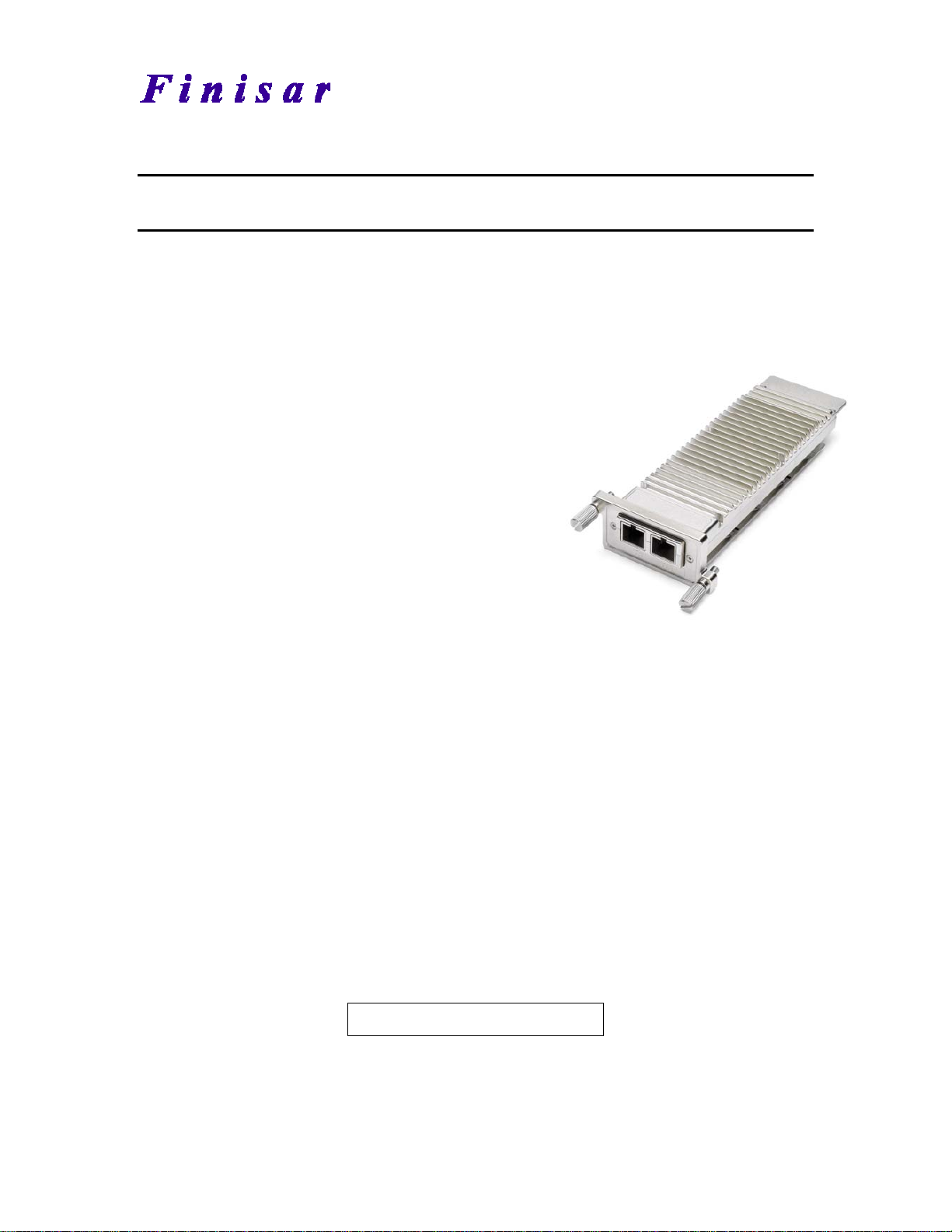
10Gb/s 1310nm Single Mode XENPAK Transponder
PRODUCT FEATURES
Hot pluggable XENPAK MSA
form factor
Total power consumption: 3.5 W
maximum
RoHS-6 compliant (lead-free)
Temperature range 0°C to 70°C
Transmission distance of 10km
Uncooled directly modulated
1310nm Distributed Feedback (DFB)
laser
SC connector, single mode fiber
Full duplex transmission mode
Digital Optics Monitoring (DOM)
Power supply: +5.0 V, +3.3 V,
Adaptable Power Supply (APS:
+1.2 V)
XAUI electrical interface
- 4 x 3.125 Gb/s Ethernet
Management and control via MDIO
2-wire bus
70-pin connector
Separated signal/chassis ground
PRODUCT SELECTION
FTLX1461E2
APPLICATIONS
10GBASE-LR 10G Ethernet
FTLX1461E2
© Finisar Corporation – October 2008 Rev B Page 1
Page 2
FTLX1461E2 Product Specification – October 2008
I. PIN DESCRIPTION
Signal Name Level I/O Pin No. Description
Management and Monitoring Ports
MDIO Open Drain I/O 17 Management Data I/O. Requires
external 10 - 22 kΩ pull-up to the
APS on host.
MDC 1.2 V
CMOS
PRTAD4 1.2 V
CMOS
PRTAD3 1.2 V
CMOS
PRTAD2 1.2 V
CMOS
PRTAD1 1.2 V
CMOS
PRTAD0 1.2 V
CMOS
LASI Open Drain O 9 Link Alarm Status Interrupt Output.
RESET Open Drain I 10 Reset Input.
Vendor Specific 11,15,16,24 Vendor Specific Pins.
TX ON/OFF Open Drain I 12 TX ON/OFF Input.
MOD DETECT O 14 Pulled low inside transponder
Transmit Functions
Reserved
Reserved
TX LANE 3–
TX LANE 3+
TX LANE 2–
TX LANE 2+
TX LANE 1–
TX LANE 1+
TX LANE 0–
TX LANE 0+
I
AC-coupled,
Internally biased
differential
XAUI
I 18 Management Data Clock Input
1 19 Port Address Input bit 4
I 20 Port Address Input bit 3
I 21 Port Address Input bit 2
I 22 Port Address Input bit 1
I 23 Port Address Input bit 0
Open Drain Compatible Output with
10 - 20 kΩ pull-up on host.
Logic high = Normal Operation
Logic low = Status Flag Triggered
Open Drain Compatible Input with
22 kΩ pull-up to APS internal to
transponder.
Logic high = Normal Operation
Logic low = RESET
Leave unconnected when not used.
Open Drain Compatible Input with
22 kΩ pull-up to APS internal to
transponder.
Logic high = Transmitter On
Logic low = Transmitter Off
through a 1 kΩ resistor to Ground
68
I
I
I
I
I
I
I
I
I
67
65
64
62
61
59
58
56
55
Reserved For Future Use
Reserved For Future Use
Module XAUI Input Lane 3–
Module XAUI Input Lane 3+
Module XAUI Input Lane 2–
Module XAUI Input Lane 2+
Module XAUI Input Lane 1–
Module XAUI Input Lane 1+
Module XAUI Input Lane 0–
Module XAUI Input Lane 0+
© Finisar Corporation – October 2008 Rev B Page 2
Page 3

FTLX1461E2 Product Specification – October 2008
Receive Functions
Reserved
Reserved
RX LANE 0+
RX LANE 0–
RX LANE 1+
RX LANE 1–
RX LANE 2+
RX LANE 2–
RX LANE 3+
RX LANE 3–
O
O
AC-coupled,
Internally biased
differential
XAUI
O
O
O
O
O
O
O
O
38
39
41
42
44
45
47
48
50
51
Reserved For Future Use
Reserved For Future Use
Module XAUI Output Lane 0+
Module XAUI Output Lane 0–
Module XAUI Output Lane 1+
Module XAUI Output Lane 1–
Module XAUI Output Lane 2+
Module XAUI Output Lane 2–
Module XAUI Output Lane 3+
Module XAUI Output Lane 3–
DC Power
GND 0 V DC 1, 2, 3, 33, 34,
35, 36, 37, 40,
Ground connection for signal ground
on the module
43, 46, 49, 52,
53, 54, 57, 60,
63, 66, 69, 70
APS +1.2 V 7, 8, 28, 29 Input from Adaptive Power Supply
APS SENSE +1.2 V 27 APS Sense Output. Connected to the
APS input inside transponder.
APS SET 25 Feedback input from APS.
Connected to GND through a 1180Ω
resistor inside the transponder.
3.3 V +3.3 V DC 5, 6, 30, 31 DC Power Input, +3.3 V DC,
Nominal
5.0 V +5.0 V DC 4, 32 DC Power Input, +5.0 V DC,
Nominal
Reserved 26 Reserved for APD.
Reserved 13 Reserved.
© Finisar Corporation – October 2008 Rev B Page 3
Page 4

FTLX1461E2 Product Specification – October 2008
Electrical Pad Layout
Fig 1-XENPAK Transponder Electrical Pad Layout
II. Absolute Maximum Ratings
Limit Values
Parameter Symbol
Storage Ambient Temperature1) TS -40 85 °C
Operating Case Temperature1) TC 0 70 °C
Supply Voltage +5.0 V V5 0 6 V
Supply Voltage +3.3 V V3 0 4 V
Supply Voltage APS V
Static Discharge Voltage, All Pins2) STd 500 V
Average Receive Optical Power RxP
Notes:
1) Non-condensing.
2) HBM
0 1.5 V
aps
1.5 dBm
max
min. max.
Unit
Exceeding any one of these values may permanently destroy the device.
© Finisar Corporation – October 2008 Rev B Page 4
Page 5

FTLX1461E2 Product Specification – October 2008
III. Electrical Characteristics
Recommended Operating Conditions
Values
Parameter Symbol
min. typ. max.
Unit
Operating Case Temperature1) TC 0 70 °C
Transponder Total Power
P 3.5 W
Consumption
Supply Voltage +5.0 V V
Supply Current +5.0 V I
Supply Voltage +3.3 V V
Supply Current +3.3 V I
Supply Voltage APS V
Supply Current APS I
1)
Worst case thermal location, see Figure 2.
See also Environmental Performance.
4.75 5.0 5.25 V
CC5
300 mA
CC5
3.14 3.3 3.47 V
CC3
300 mA
CC3
1.152 1.2 1.248 V
CC aps
1000 mA
CC aps
Electrical DC Characteristics
(V
= 4.75 V to 5.25 V, V
CC5
Parameter Symbol
1.2 V CMOS (1.8 V CMOS Compatible1)) I/O DC Characteristics
(PRTAD; LASI; RESET; TX_ONOFF)
External Pull-up Resistor for Open Drain R
Output High Voltage2) Voh 1 V
Output Low Voltage2) Vol 0.15 V
Input High Voltage Vih 0.84 1.5 V
Input Low Voltage Vil 0.36 V
Input Pull-down Current3) Ipd 20 120 µA
XAUI I/O DC Characteristics (TXLANE[0..3]; RXLANE[0. .3 ])
Differential Input Amplitude (pk-pk)
Differential Output Amplitude (pk-pk)
MDIO I/O DC Characteristics (MDIO; MDC)
Output Low Voltage5) VOL –0.3 0.2 V
Output Low Current IOL 4 mA
Input High Voltage VIH 0.84 1.5 V
Input Low Voltage VIL –0.3 0.36 V
Pull-up Supply Voltage VPU 1.152 1.2 1.248 V
Input Capacitance CIN 10 pF
Load Capacitance C
External Pull-up Resistance R
1)
For 1.8 V CMOS V
2)
R
= 10 kΩ to 1.8 V.
pull-up
3)
V
= 1.2 V.
in
4)
AC coupled.
5)
I
= 100 µA.
OL
= 1.65 V min., V
oh
= 3.14 V to 3.47 V, V
CC3
4)
V
4)
V
= 0.15 V max., V
ol
= 1.152 V to 1.248 V, TC = 0°C to 70°C)
CC aps
Values
min. typ. max.
10 22 kΩ
pullup
200 2500 mV
in_xaui
800 1600 mV
out_xaui
470 pF
LOAD
200 Ω
LOAD
= 1.17 V min., V
ih
= 0.63 V max.
il
Unit
© Finisar Corporation – October 2008 Rev B Page 5
Page 6

FTLX1461E2 Product Specification – October 2008
Electrical AC Characteristics
(V
= 4.75 V to 5.25 V, V
CC5
= 3.14 V to 3.47 V, V
CC3
= 1.152 V to 1.248 V, TC = 0°C to 70°C)
CC aps
Values
Parameter Symbol
min. typ. max.
XAUI Input AC Characteristics (TXLANE[0..3])
Baud Rate
Ethernet
Baud Rate Tolerance R
Differential Input Impedance Z
R
XAUIIN
3.125
–100 100 ppm
TOLXAUI
80 100 120 Ω
INXAUI
Gbit/s
Differential Return Loss1) |S11| 10 dB
Input Differential Skew2) t
Jitter Amplitude Tolerance3) J
75 ps
SKEWIN
0.65 UI
XAUITOL
XAUI Output AC Characteristics (RXLANE[0..3])
Baud Rate
Ethernet
Baud Rate Variation R
R
XAUIOUT
XAUIVAR
Gbit/s
3.125
–100 100 ppm
XAUI Eye Mask (far-end) According to IEEE 802.3ae
Output Differential Skew t
Output Differential Impedance Z
SKEWOUT
15 ps
80 100 120 Ω
OUTXAUI
Differential Output Return Loss1) |S22| 10 dB
Total Jitter4) TJ
Deterministic Jitter4) DJ
0.35 UI
XAUI
0.37 UI
XAUI
Power-On Reset AC Characteristics
Power-On Reset and TX_ONOFF
According to XENPAK MSA Issue 3.0, 2002-9-18
Characteristics
MDIO I/O AC Characteristics (MDIO; MDC)
MDIO Data Hold Time t
10 ns
HOLD
MDIO Data Setup Time tSU 10 ns
Delay from MDC Rising Edge to
t
300 ns
DELAY
MDIO Data Change
MDC Clock Rate ƒ
1)
100 MHz to 2.5 GHz.
2)
At crossing point.
3)
Per IEEE Std 802.3ae.
4)
At near-end, No pre-equalization, 1 UI = 320 ps.
2.5 MHz
MAX
Unit
p-p
© Finisar Corporation – October 2008 Rev B Page 6
Page 7

FTLX1461E2 Product Specification – October 2008
IV. Optical Characteristics
(V
= 4.75 V to 5.25 V, V
CC5
= 3.14 V to 3.47 V, V
CC3
= 1.152 V to 1.248 V, TC = 0°C to 70°C)
CC aps
Values
Parameter Symbol
min. typ. max.
Unit
Transmitter
Launch Power in OMA minus TDP P
Average Launch Power P
Center Wavelength Range λ
Spectral Width (-20 dB)
–5.2 dBm
O-OMA
–8.2 0.5 dBm
O-Avg
1290 1330 nm
C-Tx
σ
I
0.6 nm
Side Mode Suppression Ratio SMSR 30 dB
Extinction Ratio ER 3.5 dB
Relative Intensity Noise12OMA RIN –128 dB/Hz
Optical Modulation Aplitude (OMA) OMA –5.2 dBm
Transmitter and Dispersion Penalty TDP 3.2 dB
Average Launch Power of OFF
P
–30 dBm
O-OFF
Transmitter
Optical Return Loss Tolerance ORLT 12 dB
Transmitter Reflectance REFTX –12 dB
Eye Mask Definition According to IEEE 802.3ae
Receiver
Stressed Receiver Sensitivity in OMA P
Rx Sensitivity in OMA1) P
–10.3 dBm
IN-S
–12.6 dBm
IN-O
Average Receiver Power1) PIN -14.4 0.5 dBm
Receiver Damage Power P
Signal Detect Assert Level P
Signal Detect Hysteresis P
1.5 dBm
IN-dmg
–13 dBm
LOSa
1 dB
LOSh
Receiver Reflectance REFRX –12 dB
Receive Electrical 3dB Upper Cutoff
FC 12.3 GHz
Frequency
Center Wavelength Range λ
1260 1355 nm
C-RX
Stressed Signal Calibration
Vertical Eye Closure Penalty 2.2 dB
Stressed Eye Jitter 0.3 UIpp
1)
Average Receiver Power (min), which is defined for an ideal input signal, is informative only.
V. General Specifications
Optical Interface Standard Specifications
Standard
Differential Group Delay
Maximum (ps)
Operating Range
1)
(meters)
B1.1 SMF 10 2 to 10,000
B1.3 SMF 10 2 to 10,000
Notes:
1) Operating range as defined by IEEE standards. Longer reach possible depending upon link implementation.
© Finisar Corporation – October 2008 Rev B Page 7
Page 8

FTLX1461E2 Product Specification – October 2008
Environmental Performance
Operating case temperature: 0°C to +70°C
Operating humidity: 0% -95% RH non-condensing
Fibers and Connectors
The transponder has SC receptacles for both Tx and Rx. The transponder is designed for single
mode SC cables, 0° polished endface (PC).
70-pin Connector
The module interface connector is a 70-pin, printed circuit board edge connection with a 0.5 mm
pitch. The appropriate mating connector for the customer PCB is a 70-pin SMT, dual row, right
angled, edge connector, 0.5 mm pitch (Tyco Electronics part number 1367337-1, Molex part
number 74441-0003 or equivalent).
Rail Requirement
The XENPAK rail system required to mount the XENPAK module is fully defined by the MSA.
Aqueous Wash
Finisar XENPAK transponders are neither solderable nor aqueous washable and are not
intended for these processes.
VI. Regulatory Compliance
Feature Standard Comments
ESD:
Electrostatic Discharge to the
Electrical Pins (HBM)
Immunity:
Against Electrostatic Discharge
(ESD) to the Module Receptacle
Immunity:
Against Radio Frequency
Electromagnetic Field
Emission:
Electromagnetic Interference
(EMI)
EIA/JESD22-A114-B
(MIL-STD 883D
Method 3015.7)
EN 61000-4-2
IEC 61000-4-2
EN 61000-4-3
IEC 61000-4-3
FCC 47 CFR
Part 15, Class B
EN 55022 Class B
CISPR 22
Class 1a (> 500 V)
Discharges ranging from
the front end / faceplate / receptacle cause no
damage to module (under recommended
conditions).
With a field strength of 10 V/m, noise
frequency ranges from 10 MHz to 2 GHz. No
effect on module performance between the
specification limits.
Noise frequency range:
30 MHz to 40 GHz
Radiated emission does not exceed specified
limits when measured inside a shielding
enclosure with MSA conform cutout.
±2 kV to ±25 kV to
© Finisar Corporation – October 2008 Rev B Page 8
Page 9

FTLX1461E2 Product Specification – October 2008
Eye Safety
Finisar FTLX1461E2 transponders are Class 1 Laser Products. They are certified per the
following standards:
Feature Agency Standard Certificate
Number
Laser Eye
Safety
Laser Eye
Safety
Electrical
Safety
Electrical
Safety
FDA/CDRH CDRH 21 CFR 1040 and Laser Notice 50 9210176-104
TÜV EN 60825-1: 1994+A11:1996+A2:2001
IEC 60825-1: 1993+A1:1997+A2:2001
IEC 60825-2: 2000, Edition 2
TÜV EN 60950 R 72082131
UL/CSA
CLASS 3862.07
CLASS 3862.87
R 72082131
1439230
Copies of the referenced certificates are available at Finisar Corporation upon request.
VII. DOM Parameters
Values
Parameter
Transponder Temperature Monitor Accuracy1) -5 +5 °C
Laser Bias Current Monitor Accuracy2) -10 +10 %
Transmit Power Monitor Accuracy3) -3 +3 dB
Receive Power Monitor Accuracy3) -3 +3 dB
1)
0 to 70°C case temperature.
2)
0 to 12.5 mA.
3)
-8.2 dBm to +0.5 dBm.
min. typ. max.
Unit
VIII. Mechanical Characteristics
Values Parameter Symbol
min. typ. max.
Module Retention Force (latch strength) F
Module Insertion Force FIN 40 N
Module Extraction Force (with kick-out) F
Module Extraction Force (without kick-out) F
200 N
RET
16 N
EXT-K
25 N
EXT
Unit
© Finisar Corporation – October 2008 Rev B Page 9
Page 10
FTLX1461E2 Product Specification – October 2008
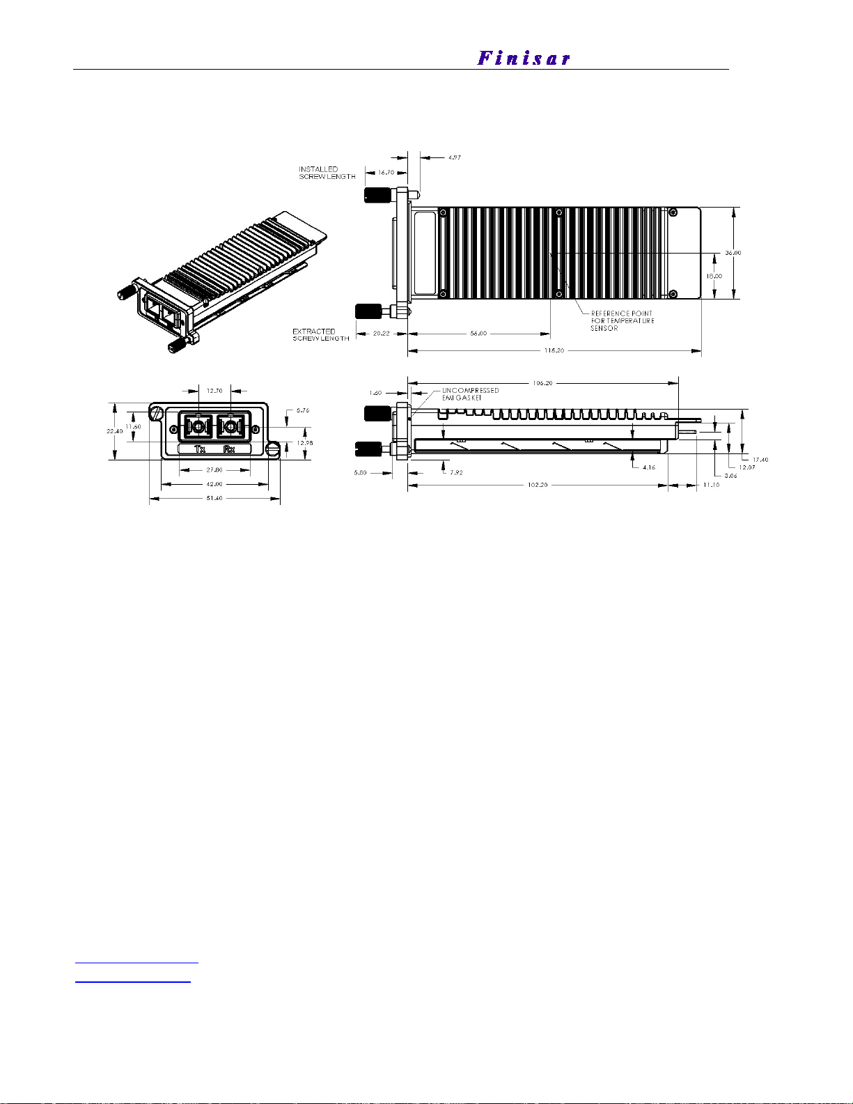
Package Outline
Figure 2-XENPAK Mechanical Dimensions
IX. References
The following references are provided for informational purposes only. The parameters and
operational behavior outlined in this specification describe the complete functionality of the 10G
Transponder. Contact Finisar for any items concerning the operational characteristics of this
device.
IEEE Std 802.3ae-2002 clause 52, 10GBASE-LR
XENPAK MSA Issue 3.0
X. For More Information
Finisar Corporation
1389 Moffett Park Drive
Sunnyvale, CA 94089-1133
Tel. 1-408-548-1000
Fax 1-408-541-6138
sales@finisar.com
www.finisar.com
© Finisar Corporation – October 2008 Rev B Page 10
 Loading...