

Page 1
Product Specification
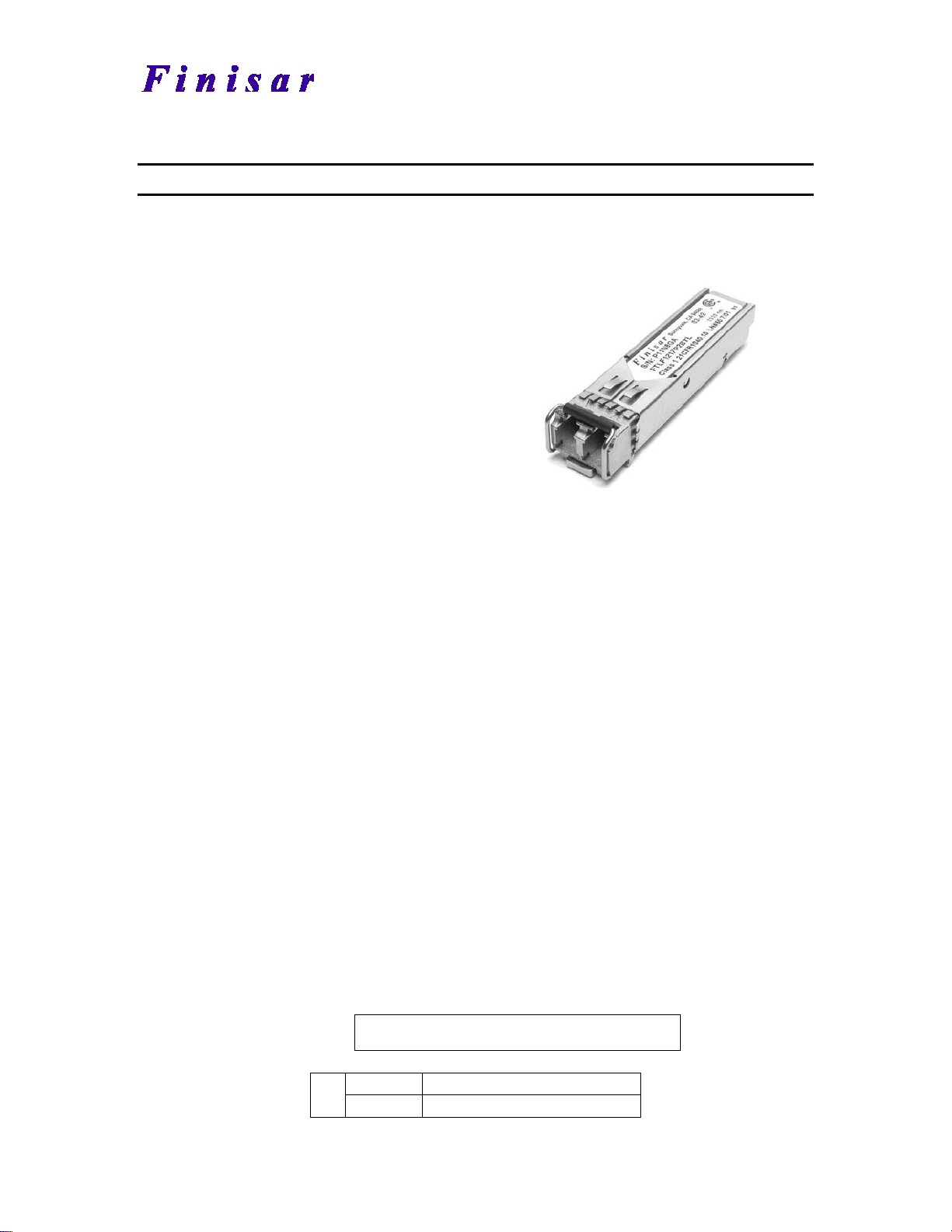
Fast Ethernet RoHS Compliant Long-Wavelength SFP Transceiver
FTLF1217P2xTL
PRODUCT FEATURES
Up to 200 Mb/s bi-directional
data links
Hot-pluggable SFP footprint
Built-in digital diagnostic functions
1310nm LED-based transmitter
Duplex LC connector
RoHS Compliant and Lead-Free
Up to 2km on 62.5/125μm MMF
Metal enclosure, for lower EMI
Single 3.3V power supply
Low power dissipation
Industrial operating temperature
range: -40°C to 85°C
Finisar’s FTLF1217P2xTL Small Form Factor Pluggable (SFP) transceivers are
compatible with the Small Form Factor Pluggable Multi-Sourcing Agreement (MSA)
They are simultaneously compatible with 100Base-FX, FDDI, ESCON, and Multimode
SONET OC-3 SR-0 and OC-1 SR-0 standards as specified in IEEE Std 802.32, ISO/IEC
9314-3
They are RoHS compliant and lead-free per Directive 2002/95/EC4 and Finisar
Application Note AN-2038. Digital diagnostics functions are available via the 2-wire
serial bus specified in the SFP MSA.
PRODUCT SELECTION
3
, Enterprise Systems Architecture/3904, and ANSI T1.416.01-19995, respectively.
APPLICATIONS
125 Mb/s 100Base-FX Ethernet /
FDDI
200 Mb/s ESCON
155 Mb/s Multimode SONET
OC-3 SR-0
51 Mb/s Multimode SONET
OC-1 SR-0
1
.
FTLF1217P2xTL
x
© Finisar Corporation September 13, 2008 Rev. B Page 1
W Wide Extraction Bail
B Narrow Extraction Bail
Page 2

FTLF1217P2xTL Pluggable SFP Product Specification – September 2008
I. Pin Descriptions
Pin Symbol Name/Description Ref.
1 V
2 T
3 T
EET
FAULT
DIS
4 MOD_DEF(2) Module Definition 2. Data line for Serial ID. 4
5 MOD_DEF(1) Module Definition 1. Clock line for Serial ID. 4
6 MOD_DEF(0) Module Definition 0. Grounded within the module. 4
7 Rate Select No connection required
8 LOS Loss of Signal indication. Logic 0 indicates normal operation. 5
9 V
10 V
11 V
12 RD-
EER
EER
EER
13 RD+ Receiver Non-inverted DATA out. AC Coupled
14 V
15 V
16 V
17 V
EER
CCR
CCT
EET
18 TD+ Transmitter Non-Inverted DATA in. AC Coupled.
19 TD20 V
EET
Notes:
1. Circuit ground is internally isolated from chassis ground.
2. T
is an open collector/drain output, which should be pulled up with a 4.7k – 10k Ohms resistor on
FAULT
the host board. Pull up voltage should be between 2.0V to Vcc + 0.3V. A high output indicates an LED
fault, i.e. LED open or short. Low indicates normal operation. In the low state, the output is pulled to
<0.8V.
3. LED output disabled on T
4. Should be pulled up with 4.7k – 10kohm s on host board to a voltage between 2.0V and 3.6V.
MOD_DEF(0) pulls line low to indicate module is plugged in.
5. LOS is open collector output. Should be pulled up with 4.7k – 10kohms on host board to a voltage
between 2.0V and 3.6V. Logic 0 indicates normal operation; logic 1 indicates loss of signal.
Transmitter Ground (Common with Receiver Ground) 1
Transmitter Fault. 2
Transmitter Disable. LED output disabled on high or open. 3
Receiver Ground (Common with Transmitter Ground) 1
Receiver Ground (Common with Transmitter Ground) 1
Receiver Ground (Common with Transmitter Ground) 1
Receiver Inverted DATA out. AC Coupled
Receiver Ground (Common with Transmitter Ground) 1
Receiver Power Supply
Transmitter Power Supply
Transmitter Ground (Common with Receiver Ground) 1
Transmitter Inverted DATA in. AC Coupled.
Transmitter Ground (Common with Receiver Ground) 1
>2.0V or open, enabled on T
DIS
<0.8V.
DIS
© Finisar Corporation September 13, 2008 Rev. B Page 2
Page 3

FTLF1217P2xTL Pluggable SFP Product Specification – September 2008
Towards
Bezel
1
2
3
4
5
6
7
8
9
10
VeeT
TXFault
TX Disable
MOD-DEF(2)
MOD-DEF(1)
MOD-DEF(0)
Rate Select
LOS
VeeR
VeeR
VeeT
TD-
TD+
VeeT
VccT
VccR
VeeR
RD+
RD-
VeeR
20
19
18
17
16
15
14
13
12
11
Towards
ASIC
Diagram of Host Board Connector Block Pin Numbers and Names
© Finisar Corporation September 13, 2008 Rev. B Page 3
Page 4

FTLF1217P2xTL Pluggable SFP Product Specification – September 2008
Δ
Δ
Δ
Δ
Δ
II. Absolute Maximum Ratings
Parameter Symbol Min Typ Max Unit Ref.
Maximum Supply Voltage Vcc -0.5 4.0 V
Storage Temperature T
Case Operating Temperature T
S
A
Relative Humidity RH 0 85 % 1
III. Electrical Characteristics (T
Parameter Symbol Min Typ Max Unit Ref.
Supply Voltage Vcc 3.0 3.6 V
Supply Current Icc 300 mA
Transmitter
Input differential impedance R
Single ended data input swing Vin,pp
Transmit Disable Voltage V
Transmit Enable Voltage V
Receiver
Single ended data output swing Vout,pp
Data output rise/fall time ≤ 155 Mb/s
LOS Fault V
LOS Normal V
Power Supply Rejection PSR
Systematic Jitter Contribution
Contributed Duty Cycle Distortion
Data Dependent Jitter Contribution
Random Jitter Contribution @ OC-3
and OC-1
Random Jitter Contribution @ FE
Notes:
1. Non condensing.
2. Connected directly to TX data input pins. AC coupling from pins into driver IC.
3. We recommend <600mV for best EMI performance.
4. Or open circuit.
5. Into 100 ohms differential termination.
6. 10 – 90 %
7. LOS is an open collector output. Should be pulled up with 4.7k – 10kohms on the host board. Normal
operation is logic 0; loss of signal is logic 1. Maximum pull-up voltage is 5.5V.
8. Receiver sensitivity is compliant with power supply sinusoidal modulation of 20 Hz to 1.5 MHz up to
specified value applied through the recommended power supply filtering network.
9. Peak-to-peak measurement for OC-3 SR-0 or OC-1 SR-0 operation measured with a PRBS 2
pattern.
10. Peak-to-peak measurement based on 4B/5B encoded Fast Ethernet pattern referenced in FDDI PMD
Annex A.5
= -40 to 85 °C, VCC = 3.0 to 3.6 Volts)
A
in
D
EN
t
r/tf
LOS fault
LOS norm
RX
SJ
RX
DCD
RX
DDJ
RX
RJ
RX
RJ
-40 85
-40 85
100
250 1200 mV 3
2 Vcc V 4
Vee Vee+ 0.8 V
250 450 900 mV 5
0.6 5.0 ns 6
2 Vcc
Vee Vee+0.5 V 7
100 mVpp 8
2.0 ns 9
1.0 ns 10
1.2 ns 10
0.6 ns 9
0.76 ns 10
HOST
°C
°C
Ω
2
V 7
23
-1 test
3
© Finisar Corporation September 13, 2008 Rev. B Page 4
Page 5

FTLF1217P2xTL Pluggable SFP Product Specification – September 2008
Δ
Δ
Δ
Δ
IV. Optical Characteristics (T
Parameter Symbol Min Typ Max Unit Ref.
Transmitter
Output Opt. Power P
Optical Wavelength
Spectral Width (FWHM)
Optical Rise/Fall Time ≤ 155 Mb/s
Optical Rise/Fall Time = 200 Mb/s tr/ t
Systematic Jitter Contribution
Contributed Duty Cycle Distortion
Data Dependent Jitter Contribution
Random Jitter Contribution @ OC-3
and OC-1
Random Jitter Contribution @ FE
Extinction Ratio ER 10 dB
Receiver
Receiver Sensitivity = 51.8 Mb/s RxSENS -30 dBm 7
Receiver Sensitivity = 155 Mb/s RxSENS -30 dBm 7
Receiver Sensitivity = 125 Mb/s RxSENS -31 dBm 7
Receiver Sensitivity = 200 Mb/s RxSENS -29 dBm 8
Maximum Average Receiver Power Rx
Optical Center Wavelength
LOS De-Assert LOS
LOS Assert LOS
LOS Hysteresis
Notes:
1. Measured average power coupled into 62.5/125um fibre with NA = 0.275. Class 1 eye safety per
FDA/CDRH, IEC, and EN60825-1 safety standards.
2. Also specified to fall within the extrapolated curves in FDDI PMD
between wavelength, spectral width and transmitter rise/fall times.
3. Unfiltered, 10-90%.
4. Unfiltered, 20-80%.
5. Peak-to-peak measurement for OC-3 SR-0 or OC-1 SR-0 operation measured with a PRBS 2^23-1 test
pattern.
6. Peak-to-peak measurement based on 4B/5B encoded Fast Ethernet pattern referenced in FDDI PMD
Annex A.5
7. Specifications are for 50 micro-meter or 62.5 micro-meter fiber.
8. Specifications are for 50 micro-meter or 62.5 micro-meter fiber, based on any valid 8B/10B code
pattern and measured at, or extrapolated to, 10
= -40 to 85 °C, VCC = 3. 00 to 3.60 Volts)
OP
OUT
λ
σ
t
/ t
r
f
f
TX
SJ
TX
DCD
TXΔDDJ
TX
RJ
TX
RJ
-20 -15 dBm 1
1280 1380 nm
175 nm 2
0.6 3.0 ns 3
1.7 ns 4
1.6 ns 5
1.0 ns 6
0.6 ns 6
0.6 ns 5
0.76 ns 6
MAX
λ
C
D
A
-15
-14 dBm
1270 1600 nm
-33 dBm
-45 dBm
1.5 dB
3
Figure 9, which allow trade-off
BER.
3
© Finisar Corporation September 13, 2008 Rev. B Page 5
Page 6

FTLF1217P2xTL Pluggable SFP Product Specification – September 2008
V. General Specifications
Parameter Symbol Min Typ Max Units Ref.
Data Rate BR 51.8,
155,
125,
200
Bit Error Rate BER 10
Max. Supported Link Length on
L
MAX1
3 km 2
50/125μm or 62.5 μm MMF @ OC-1
Max. Supported Link Length on
L
MAX2
2 km 3
50/125μm or 62.5 μm MMF @ OC-3
Max. Supported Link Length on
L
MAX3
2 km 4
50/125μm or 62.5 μm MMF @ FE
Max. Supported Link Length on
L
MAX4
2 km 5
50/125μm or 62.5 μm MMF @ ESCON
Notes:
1. Multimode SONET OC-1 SR-0 and OC-3 SR -0, 100Base-FX and FDDI compliant as specified in
ANSI T1.416.01-1999
specified in Enterprise Systems Architecture/390
5
, IEEE Std 802.32, and ISO/IEC 9314-33 respectively. ESCON compatible as
4
.
2. At 51.8 Mb/s data rate per ANSI T1.416.01-19995.
3. At 155 Mb/s data rate per ANSI T1.416.01-19995.
4. At 125 Mb/s data rate per ISO/IEC 9314-3
3
5. At 200 Mb/s data rate per Enterprise Systems Architecture/3904.
VI. Environmental Specifications
Finisar 1310nm SFP transceivers have an industrial operating temperature range from
–40°C to +85°C case temperature.
Parameter Symbol Min Typ Max Units Ref.
Case Operating Temperature T
Storage Temperature T
op
sto
-40 85 °C
-40 85 °C
VII. Regulatory Compliance
Finisar transceivers are Class 1 eye safety products and comply with US FDA
regulations. These products are certified by TÜV and CSA to meet the Class 1 eye safety
requirements of EN (IEC) 60825 and the electrical safety requirements of
EN (IEC) 60950. Copies of certificates are available at Finisar Corporation upon request.
Copies of the referenced certificates are available at Finisar Corporation upon request.
Mb/sec 1
-10
© Finisar Corporation September 13, 2008 Rev. B Page 6
Page 7

FTLF1217P2xTL Pluggable SFP Product Specification – September 2008
VIII. Digital Diagnostic Functions
Finisar FTLF1217P2xTL SFP transceivers support the 2-wire serial communication
protocol as defined in the SFP MSA1. It is very closely related to the E2PROM defined in
the GBIC standard, with the same electrical specifications.
The standard SFP serial ID provides access to identification information that describes
the transceiver’s capabilities, standard interfaces, manufacturer, and other information.
Additionally, Finisar SFP transceivers provide a unique enhanced digital diagnostic
monitoring interface, which allows real-time access to device operating parameters such
as transceiver temperature, bias current, transmitted optical power, received optical
power and transceiver supply voltage. It also defines a sophisticated system of alarm and
warning flags, which alerts end-users when particular operating parameters are outside of
a factory set normal range.
The SFP MSA defines a 256-byte memory map in E2PROM that is accessible over a
2-wire serial interface at the 8 bit address 1010000X (A0h). The digital diagnostic
monitoring interface makes use of the 8 bit address 1010001X (A2h), so the originally
defined serial ID memory map remains unchanged. The interface is identical to, and is
thus fully backward compatible with both the GBIC Specification and the SFP Multi
Source Agreement. The complete interface is described in Finisar Application Note AN2030: “Digital Diagnostics Monitoring Interface for SFP Optical Transceivers”.
The operating and diagnostics information is monitored and reported by a Digital
Diagnostics Transceiver Controller (DDTC) inside the transceiver, which is accessed
through a 2-wire serial interface. When the serial protocol is activated, the serial clock
signal (SCL, Mod Def 1) is generated by the host. The positive edge clocks data into the
SFP transceiver into those segments of the E2PROM that are not write-protected. The
negative edge clocks data from the SFP transceiver. The serial data signal (SDA, Mod
Def 2) is bi-directional for serial data transfer. The host uses SDA in conjunction with
SCL to mark the start and end of serial protocol activation. The memories are organized
as a series of 8-bit data words that can be addressed individually or sequentially.
For more information, please see the SFP MSA documentation
Note AN-2030.
Please note that evaluation board FDB-1018 is available with Finisar ModDEMO
software that allows simple to use communication over the 2-wire serial interface.
1,7
or Finisar Application
© Finisar Corporation September 13, 2008 Rev. B Page 7
Page 8

FTLF1217P2xTL Pluggable SFP Product Specification – September 2008
IX. Digital Diagnostic Specifications
FTLF1217P2xTL transceivers have internally calibrated digital diagnostics.
Parameter Symbol Min Typ Max Units Ref.
Accuracy
Internally measured transceiver
DD
Temperature
± 3
ºC
temperature
Internally measured transceiver
DD
Voltage
± 100
mV
supply voltage
Measured TX bias current
Measured TX output power
Measured RX received average
DD
DD
DD
Tx-Power
Rx-Power
Bias
± 10
± 3
± 3
%
dB
dB
optical power
Dynamic Range for Rated Accuracy
Internally measured transceiver
DD
Temperature
-40 85 ºC
temperature
Internally measured transceiver
DD
Voltage
3.0 3.6 V
supply voltage
Measured TX bias current
Measured TX output power
Measured RX received average
DD
DD
DD
Tx-Power
Rx-Power
Bias
0 70 mA
-22 -13 dBm
-33 -12 dBm
optical power
Max Reporting Range
Internally measured transceiver
DD
Temperature
-40 125 ºC
temperature
Internally measured transceiver
DD
Voltage
2.8 4.0 V
supply voltage
Measured TX bias current
Measured TX output power
Measured RX received average
DD
DD
DD
Tx-Power
Rx-Power
Bias
0 80
mA
-24 -11 dBm
-35 -10 dBm
optical power
Notes:
1. Accuracy of Measured Tx Bias Current is 10% of the actual Bias Current from the driver to the LED.
1
© Finisar Corporation September 13, 2008 Rev. B Page 8
Page 9

FTLF1217P2xTL Pluggable SFP Product Specification – September 2008
X. Mechanical Specifications
Finisar’s Small Form Factor Pluggable (SFP) transceivers are compatible with the
dimensions defined by the SFP Multi-Sourcing Agreement (MSA).
FTLF1217P2BTL
© Finisar Corporation September 13, 2008 Rev. B Page 9
Page 10

FTLF1217P2xTL Pluggable SFP Product Specification – September 2008
FTLF1217P2WTL
© Finisar Corporation September 13, 2008 Rev. B Page 10
Page 11

FTLF1217P2xTL Pluggable SFP Product Specification – September 2008
XI. PCB Layout and Bezel Recommendations
© Finisar Corporation September 13, 2008 Rev. B Page 11
Page 12

FTLF1217P2xTL Pluggable SFP Product Specification – September 2008
© Finisar Corporation September 13, 2008 Rev. B Page 12
Page 13

FTLF1217P2xTL Pluggable SFP Product Specification – September 2008
XII. References
1. Small Form-factor Pluggable (SFP) Transceiver Multi-source Agreement (MSA).
September 14, 2000.
2. IEEE Std 802.3, 2002 Edition, Clause 38, PMD Type 1000BASE-LX.
IEEE Standards Department, 2002.
3. ISO/IEC 9314-3. “Information Processing Systems – Fibre Distributed Data
Interface (FDDI), Part 3, Phystical Layer Medium Dependent (PMD).” 1990.
4. Enterprise Systems Architecture/390, ESCON I/O Interface, Physical Layer. IBM
Corp., Third Edition, 1996.
5. ANSI T1.416.01-1999. “Network to Customer Installation Interfaces – Synchronous
Optical NETwork (SONET) Physical Media Dependent Specification: Multi-Mode
Fiber.” ANSI, 1999.
6. Directive 2002/95/EC of the European Council Parliament and of the Council, “on
the restriction of the use of certain hazardous substances in electrical and electronic
equipment.” January 27, 2003.
7. “Digital Diagnostics Monitoring Interface for Optical Transceivers”. SFF Document
Number SFF-8472, Revision 9.3.
XIII. For More Information
Finisar Corporation
1389 Moffett Park Drive
Sunnyvale, CA 94089-1133
Tel. 1-408-548-1000
Fax 1-408-541-6138
sales@finisar.com
www.finisar.com
© Finisar Corporation September 13, 2008 Rev. B Page 13
 Loading...