

Page 1
Finisar
Product Specification
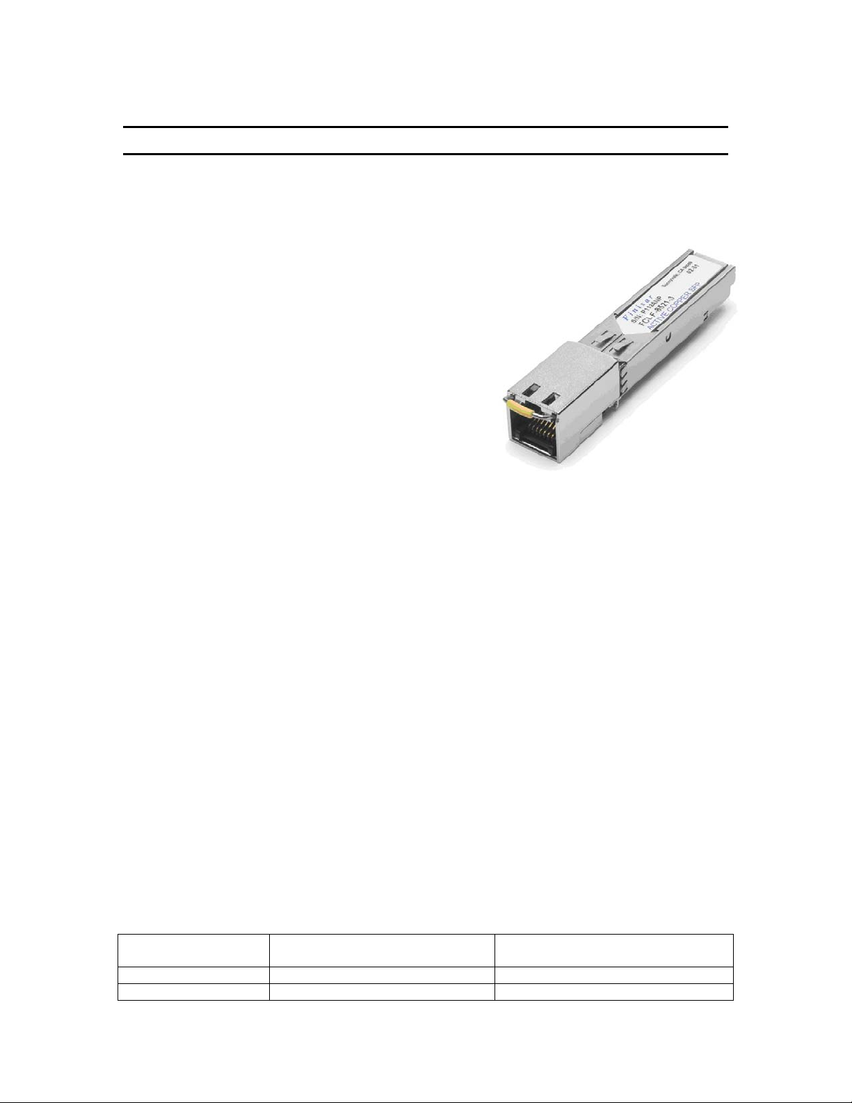
1000BASE-T Copper SFP Transceiver
FCLF-8520/8521-3
Product Features
• Up to 1.25Gb/s bi-directional data links
• Hot-pluggable SFP footprint
• Extended case temperature
range (0°C to +85°C )
• Fully metallic enclosure for low EMI
• Low power dissipation (1.05 W typical)
• Compact RJ-45 connector assembly
• RoHS compliant and Lead Free
• Access to physical layer IC via 2-wire
serial bus
• 10/100/1000 BASE-T operation in host
systems with SGMII interface
Finisar’s FCLF-8520/8521-3 1000BASE-T Copper Small Form Pluggable (SFP)
transceivers are based on the SFP Multi Source Agreement (MSA)1. They are compatible
with the Gigabit Ethernet and 1000BASE-T standards as specified in IEEE Std 802.3
The 1000BASE-T physical layer IC (PHY) can be accessed via I2C, allowing access to
all PHY settings and features.
The FCLF-8520-3 uses the SFP’s RX_LOS pin for link indication, and 1000BASE-X
auto-negotiation should be disabled on the host system. The FCLF-8521-3 is compatible
with 1000BASE-X auto-negotiation, but does not have a link indication feature
(RX_LOS is internally grounded). See AN-2036, “Frequently Asked Questions
Regarding Finisar’s 1000BASE-T SFPs”, for a more complete explanation on the
differences between the two models and details on applications issues for the products.
PRODUCT SELECTION
Part Number Link Indicator on RX_LOS Pin 1000BASE-X auto-negotiation
FCLF-8520-3 Yes No
FCLF-8521-3 No Yes
Applications
• 1.25 Gigabit Ethernet over Cat
5 cable
enabled by default
2
.
© Finisar Corporation December 16, 2005 RevB Page 1
Page 2

FCLF-8520/8521-3 1000BASE-T SFP Product Specification Finisar
I. SFP to Host Connector Pin Out
Pin Symbol Name/Description Note
1 V
2 T
3 T
EET
FAULT
DIS
4 MOD_DEF(2) Module Definition 2. Data line for serial ID 3 5 MOD_DEF(1) Module Definition 1. Clock line for serial ID 3 6 MOD_DEF(0) Module Definition 0. Grounded wi t hin t he module 3 7 Rate Select No connection required 8 LOS Loss of Signal indication. 4
9 V
10 V
11 V
12 RD-
EER
EER
EER
13 RD+ Receiver Non-inverted DATA out. AC coupled
14 V
15 V
16 V
17 V
EER
CCR
CCT
EET
18 TD+ Transmitter Non-Inverted DATA in. AC coupled
19 TD20 V
EET
Notes: 1. Circuit ground is connected to chassis ground
2. PHY disabled on T
3. Should be pulled up with 4.7k – 10k Ohms on host board to a voltage between 2.0 V and 3.6 V.
MOD_DEF(0) pulls line low to indicate module is plugged in.
4. LVTTL compatible with a maximum voltage of 2.5V. Not supported on FCLF-8521-3.
Table 1. SFP to host connector pin assignments and descriptions
Transmitter ground (common with receiver ground) 1
Transmitter Fault. Not supported
Transmitter Disable. PHY disabled on high or open 2
Receiver ground (common with transmitter ground) 1
Receiver ground (common with transmitter ground) 1
Receiver ground (common with transmitter ground) 1
Receiver Inverted DATA out. AC coupled
Receiver ground (common with transmitter ground) 1
Receiver power supply
Transmitter power supply
Transmitter ground (common with receiver ground) 1
Transmitter Inverted DATA in. AC coupled
Transmitter ground (common with receiver ground) 1
> 2.0V or open, enabled on T
DIS
< 0.8V
DIS
Towards
Bezel
1
2
3
4
5
6
7
8
9
10
VeeT
TXFault
TX Disable
MOD-DEF(2)
MOD-DEF(1)
MOD-DEF(0)
Rate Select
LOS
VeeR
VeeR
VeeT
TD-
TD+
VeeT
VccT
VccR
VeeR
RD+
RD-
VeeR
20
19
18
17
16
15
14
13
12
11
Towards
ASIC
Figure 1. Diagram of host board connector block pin numbers and names
© Finisar Corporation December 16, 2005 RevB Page 2
Page 3
FCLF-8520/8521-3 1000BASE-T SFP Product Specification Finisar
p
II. +3.3V Volt Electrical Power Interface
The FCLF-8520/8521-3 has an input voltage range of 3.3 V +/- 5%. The 4 V maximum
voltage is not allowed for continuous operation.
+3.3 Volt Electrical Power
Interface
Parameter Symbol Min Typ Max Units Notes/Conditions
Supply Current I
Input Voltage V
s
cc
320 375 mA 1.2W max power over
full range of voltage
and temperature.
See caution note below
3.13 3.3 3.47 V Referenced to GND
Maximum Voltage V
Surge Current I
Caution: Power consumption and surge current are higher than the specified values in the SFP MSA
max
surge
Table 2. +3.3 Volt electrical
4 V
30 mA Hot plug above steady state
current. See caution note
below
ower interface
III. Low-Speed Signals
MOD_DEF(1) (SCL) and MOD_DEF(2) (SDA), are open drain CMOS signals (see
section VII, “Serial Communication Protocol”). Both MOD_DEF(1) and MOD_DEF(2)
must be pulled up to host_Vcc.
Low-Speed Signals,
Electronic Characteristics
Parameter Symbol Min Max Units Notes/Conditions
SFP Output LOW V
SFP Output HIGH V
SFP Input LOW V
SFP Input HIGH V
OL
OH
IL
IH
Table 3. Low-speed signals, electronic characteristics
0 0.5 V 4.7k to 10k pull-up to host_Vcc,
measured at host side of connector
host_Vcc - 0.5 host_Vcc + 0.3 V 4.7k to 10k pull-up to host_Vcc,
measured at host side of connector
0 0.8 V 4.7k to 10k pull-up to Vcc,
measured at SFP side of connector
2 Vcc + 0.3 V 4.7k to 10k pull-up to Vcc,
measured at SFP side of connector
© Finisar Corporation December 16, 2005 RevB Page 3
Page 4

FCLF-8520/8521-3 1000BASE-T SFP Product Specification Finisar
IV. High-Speed Electrical Interface
All high-speed signals are AC-coupled internally.
High-Speed Electrical
Interface,
Transmission Line-SFP
Parameter Symbol Min Typ Max Units Notes/Conditions
Line Frequency f
L
125 MHz 5-level encoding, per
IEEE 802.3
Tx Output Impedance Z
out,TX
100 Ohm Differential, for all
frequencies between
1MHz and 125MHz
Rx Input Impedance Z
in,RX
100 Ohm Differential, for all
frequencies between
1MHz and 125MHz
Table 4. High-speed electrical interface, transmission line-SFP
High-Speed Electrical Interface,
Host-SFP
Parameter Symbol Min Typ Max Units Notes/Conditions
Single ended data input
swing
Single ended data output
swing
Rise/Fall Time Tr,T
Tx Input Impedance Z
Rx Output Impedance Z
V
V
insing
outsing
f
in
out
250 1200 mV Single ended
350 800 mV Single ended
175 psec 20%-80%
50 Ohm Single ended
50 Ohm Single ended
Table 5. High-speed electrical interface, host-SFP
© Finisar Corporation December 16, 2005 RevB Page 4
Page 5

FCLF-8520/8521-3 1000BASE-T SFP Product Specification Finisar
V. General Specifications
General
Parameter Symbol Min Typ Max Units Notes/Conditions
Data Rate BR 10 1,000 Mb/sec IEEE 802.3 compatible.
Cable Length L 100 m Category 5 UTP. BER <10
Table 6. General specifications
See Notes 2 through 4 below
-12
Notes:
1. Clock tolerance is +/- 50 ppm
2. By default, the FCLF-8520/8521-3 is a full duplex device in preferred master mode
3. Automatic crossover detection is enabled. External crossover cable is not required
4. 10/100/1000 BASE-T operation requires the host system to have an SGMII interface
with no clocks, and the module PHY to be configured per Application Note AN-2036.
With a SERDES that does not support SGMII, the module will operate at 1000BASE-T
only.
VI. Environmental Specifications
The FCLF-8520/8521-3 has an extended range from 0°C to +85°C case temperature as
specified in Table 8.
Environmental
Specifications
Parameter Symbol Min Typ Max Units Notes/Conditions
Operating Temperature T
Storage Temperature T
op
sto
0 85 °C Case temperature
-40 85 °C Ambient temperature
Table 7. Environmental specifications
VII. Serial Communication Protocol
All Finisar SFPs support the 2-wire serial communication protocol outlined in the SFP
MSA1. These SFPs use an Atmel AT24C01A 128 byte E2PROM with an address of A0h.
For details on interfacing with the E2PROM, see the Atmel data sheet titled
“AT24C01A/02/04/08/16 2-Wire Serial CMOS E
2
PROM.”3
The 1000BASE-T physical layer IC can also be accessed via the 2-wire serial bus at
address ACh. For details interfacing with the PHY IC, see Marvell data sheet titled
4
“Alaska Ultra 88E1111 Integrated Gigabit Ethernet Transceiver”
(Marvell document
number MV-S100649-00).
© Finisar Corporation December 16, 2005 RevB Page 5
Page 6

FCLF-8520/8521-3 1000BASE-T SFP Product Specification Finisar
Serial Bus Timing
Requirements
Parameter Symbol Min Typ Max Units Notes/Conditions
I2C Clock Rate
0 100,000 Hz
Table 8. Serial bus timing requirements
VIII. Mechanical Specifications
The host-side of the FCLF-8520/8521-3 conforms to the mechanical specifications
outlined in the SFP MSA1. The front portion of the SFP (part extending beyond the face
plate of the host) is larger to accommodate the RJ-45 connector. See Figure 2 below for
details.
Figure 2. FCLF-8520/8521-3 mechanical dimensions
© Finisar Corporation December 16, 2005 RevB Page 6
Page 7

FCLF-8520/8521-3 1000BASE-T SFP Product Specification Finisar
IX. References
1. Small Form Factor Pluggable (SFP) Transceiver Multi-Source Agreement (MSA),
September 2000. Documentation is currently available at Finisar upon request.
2. IEEE Std 802.3, 2002 Edition. IEEE Standards Department, 2002.
4. “AT24C01A/02/04/08/16 2-Wire Serial CMOS E2PROM”, Atmel Corporation.
www.Atmel.com
5. “Alaska Ultra 88E1111 Integrated 10/100/1000 Gigabit Ethernet Transceiver”,
Marvell Corporation. www.marvell.com
X. For More Information
Finisar Corporation
1389 Moffett Park Drive
Sunnyvale, CA 94089-1133
Tel. 1-408-548-1000
Fax 1-408-541-6138
sales@finisar.com
www.finisar.com
© Finisar Corporation December 16, 2005 RevB Page 7
 Loading...