

Filtronic LP3000, LPV3000 User Manual
)
查询LP3000供应商
Filtronic LP3000/LPV3000
Solid State
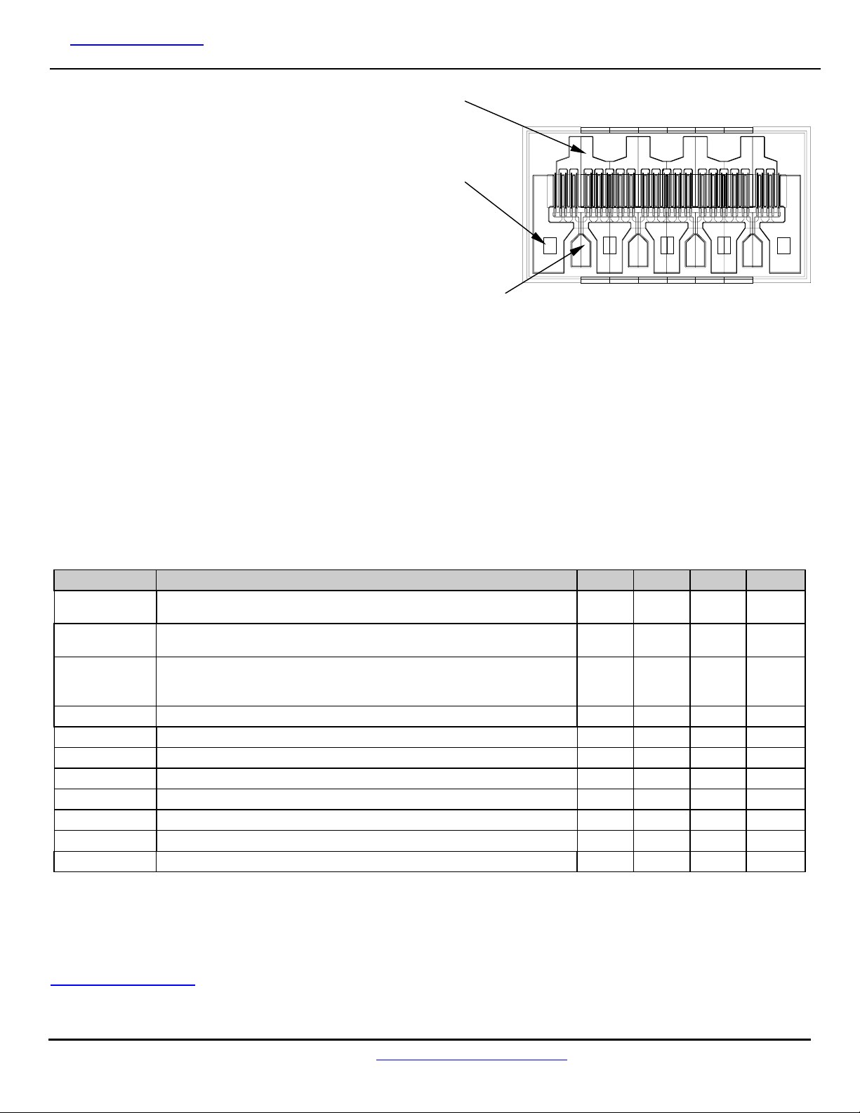
DRAIN PAD
(x4)
2W Power PHEMT
FEATURES
•
+33.5 dBm Typical Power at 18 GHz
•
7 dB Typical Power Gain at 18 GHz
•
+30.5 dBm at 3.3V Battery Voltage
•
Low Intermodulation Distortion
•
45% Power-Added-Efficiency at 18 GHz
SOURCE BOND
PAD (x2)
GATE PAD
(x4)
DIE SIZE: 28.3 x 16.5 mi l s (720 x 420 µm)
DIE THICKNESS: 2.6 mils (65 µm typ.)
BONDING PADS: 1.9 x 2.4 mi l s (50 x 60 µm typ.)
DESCRIPTION AND APPLICATIONS
The LP3000 is an Aluminum Gallium Arsenide / Indium Gallium Arsenide (AlGaAs/InG aAs) Ps eudomor phic High Electron
Mobility Transistor (PHEMT), utilizing an Electron-Beam direct-write 0.25 µm by 3000 µm Schottky barrier gate. The
recessed “mus hroom” gate structure minim izes parasitic gate-source and gate resistances. The epitaxial structure and
processing have been optimized for reliable high-power applications. T he LP3000 also features Si
available with plated source via-holes (LPV 3000) as an option for improved high-frequency performance. Also available in
a ceramic flanged package (P100) and ball grid array package.
Typical applications include commercial and military high-performance power amplifiers, including SATCOM uplink
transmitters, PCS/Cellular low-voltage high-ef ficiency output amplifiers, and medium -haul digital radio transmitters. The
LPV 3000/LP 3000 may be procured in a variety of grades, depending upon specific user requirements. Standard lot
screening is patterned after MIL-STD-19500, JANC grade. Space-level screening to FSS JANS grade is also available.
passivation and is
3N4
PERFORMANCE SPECIFICATIONS (TA = 25°C)
SYMBOLS PARAMETERS MIN TYP MAX UNITS
I
P
G
η
I
G
I
BV
BV
DSS
1dB
1dB
ADD
MAX
V
GSO
Θ
M
P
GS
GD
J
Saturated Drain-Source Current
= 2V VGS = 0V
V
DS
Output Power at 1dB Gain Compression
= 8.0V, IDS = 50% I
V
DS
Power Gain at 1dB Gain Compression
= 8.0V, IDS = 50% I
V
DS
V
= 8.0V, IDS = 50% I
DS
Power-Added Efficiency (typ. for Class A operation
Maximum Drain-Source Current VDS = 2V VGS = +1V 1700 mA
Transconductance VDS = 2V VGS = 0V 725 900 mS
Pinch-Off Voltage VDS = 2V IDS = 10mA -0.25 -1.2 -2.0 V
Gate-Source Leakage Current VGS = -5V 15 125
Gate-Source Breakdown Voltage IGS = 15mA -12 -15 V
Gate-Drain Breakdown Voltage IGD = 15mA -12 -16 V
Thermal Resistivity 20
(LP. LPV) f = 18 GHz 33.0 33.5 dBm
DSS
(LP) f = 18 GHz
DSS
(LPV) f = 18 GHz
DSS
800 1060 1100 mA
4.0
6.0
6.0
7.0
45 %
dB
dB
µ
°
C/W
A
Get Curtice Model
Phone:
(408) 988-1845
Internet:
DSS-027 WG
http://www.filtronicsolidstate.com
Fax:
(408) 970-9950
Filtronic LP3000/LPV3000
Solid State
ABSOLUTE MAXIMUM RATINGS
(25°C)
SYMBOL PARAMETER RATING
V
DS
V
GS
I
DS
I
G
P
IN
T
CH
T
STG
P
T
Drain-Source Voltage 12V V
Gate-Source Voltage -5V V
Drain-Source Current 2 x I
Gate Current 120 mA I
RF Input Power 1.2 W P
Channel Temperature
Storage Temperature
175°C
-65/175°C
Power Dissipation 6.0W
DSS
3,4
RECOMMENDED CONTINUOUS
1
SYMBOL PARAMETER RATING
DS
GS
I
DS
G
IN
T
CH
T
STG
P
T
G
XdB
OPERATING LIMITS
Drain-Source Voltage 8V
Gate-Source Voltage -1V
Drain-Source Current 0.8 x I
Gate Current 40 mA
RF Input Power 600 mW
Channel Temperature
Storage Temperature
Power Dissipation 5.0 W
Gain Compression 8 dB
2W Power PHEMT
DSS
150°C
-20/50°C
NOTES:
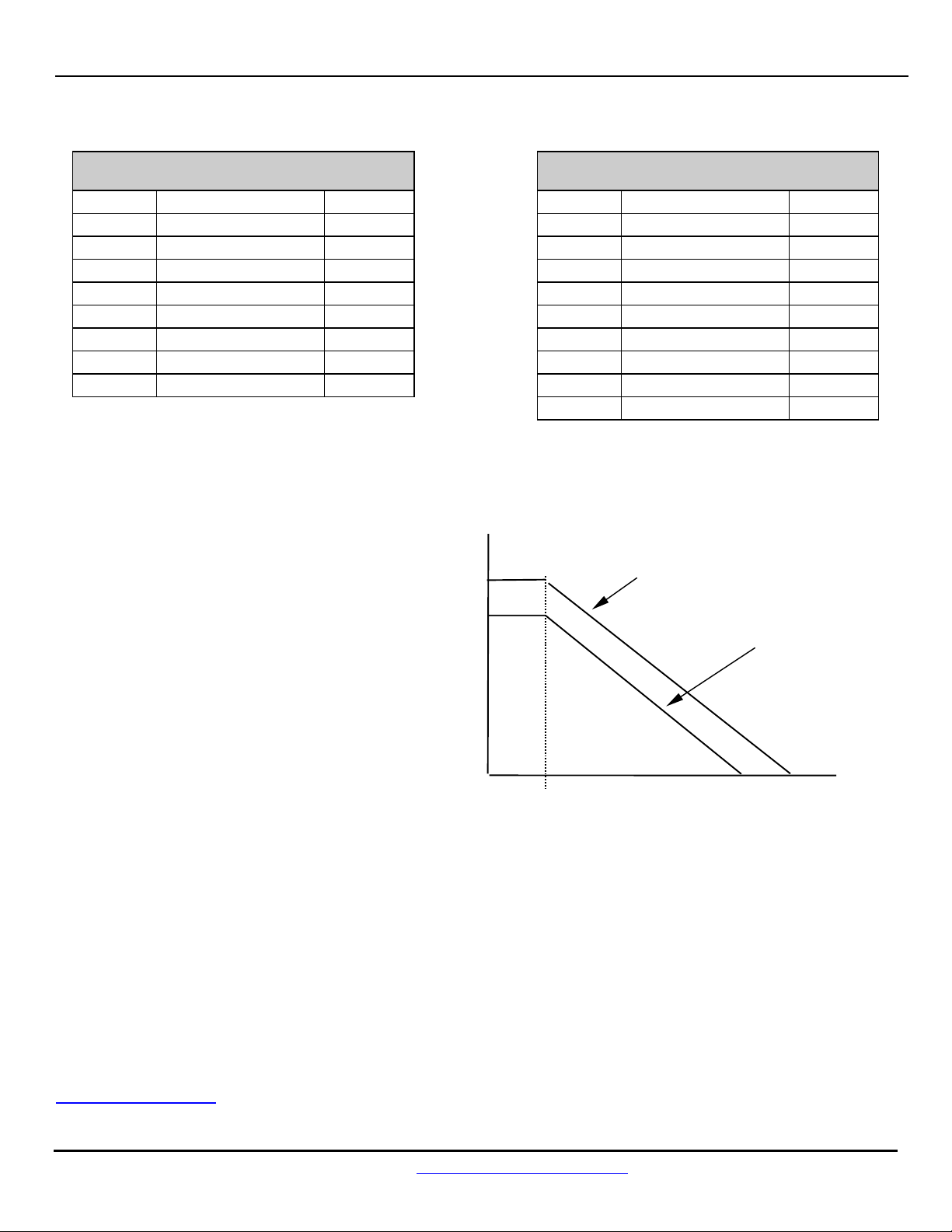
1. Operating conditions that exceed the Absolute Maximum Ratings could result in permanent damage to the device.
2. Recommended Continuous Operating Limits should be observed for reliable device operation.
3. Power Dissipation defined as: P
= RF input power.
P
IN
≡ (PDC + PIN) - P
T
4. Power Dissipation to be de-rated as follows:
, where: PDC = DC bias power, P
OUT
PT(W)
= RF output power, and
OUT
5. Specifications subject to change without notice.
Example #1 :
= 8V, IDS = 535 mA
V
DS
= P
P
IN
= 0 dBm (quiescent condition):
OUT
= PDC = 4.28W
P
T
Max. continuous T
= 25°C
HS
6.0
5.0
-40 mW/°C
-40 mW/°C
2
3,4
Example #2:
= 8V, IDS = 535 mA
V
DS
= 26.5 dBm P
P
IN
= (4.28+0.45) - 2.24 = 2.49W
P
T
Max. continuous T
HANDLING PRECAUTIONS:
= 33.5 dBm
OUT
= 88°C
HS
25
150
175
THS(°C)
PHEMT chips should be stored in a dry nitrogen environm ent until as sembly. Care should be exercised dur ing handling to
avoid damage to the devices. Proper Electrostatic Discharge (ESD) precautions should be observed at all stages of
storage, handling, assembly, and testing. These devic es should be treated as Clas s 1A (0- 500V), and f urther inform ation
on ESD control measures can be found in MIL-STD-1686 and MIL-HDBK-263.
ASSEMBLY INSTRUCTIONS:
The recomm ended die attach is gold/tin eutectic s older under a nitrogen atm osphere. Stage temperatur e should be 280290°C; maximum time at temperature is 1 min. The recommended wire bond method is thermo-compression wedge
bonding with 0.7 or 1.0 mil (0.018 or 0.025 mm) gold wire. Stage temperature should be 250-260°C.
APPLICATIONS NOTES AND DESIGN DATA:
Applications Notes are available from your local FSS Sales Repres entative, or directly from the factory. Complete design
data, including S-parameters, Noise data, and Large-Signal models, is available on 3.5” disk ette, or may be down-loaded
from our Web Page.
Get Curtice Model
DSS-027 WG
Phone:
(408) 988-1845
Internet:
http://www.filtronicsolidstate.com
Fax:
(408) 970-9950
 Loading...