

Filtronic LP3000P100 User Manual
DSS
查询LP3000P100供应商
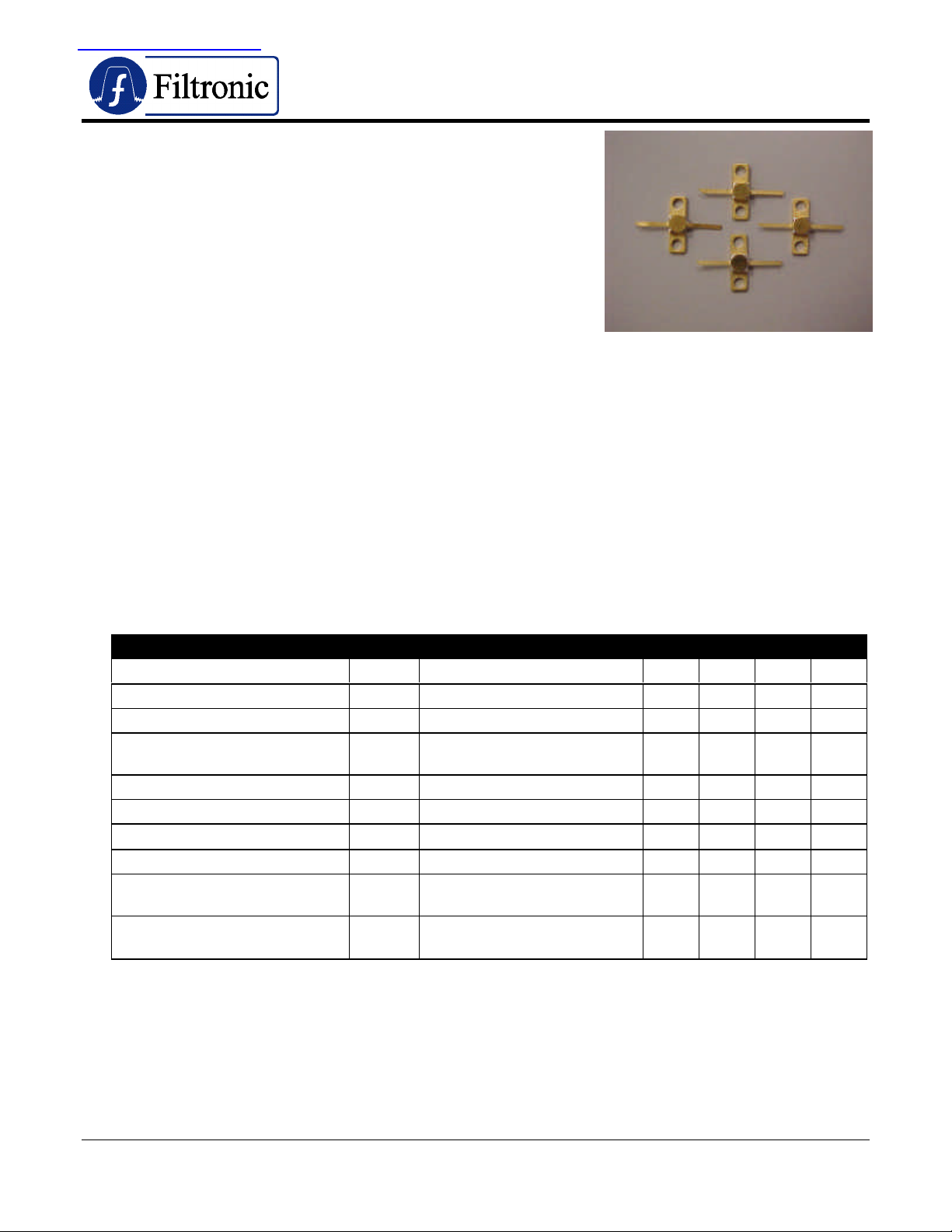
LP3000P100
PACKAGED 2W POWER PHEMT
• FEATURES
♦ 33 dBm Output Power at 1-dB Compression at 15 GHz
♦ 8 dB Power Gain at 15 GHz
♦ 60% Power-Added Efficiency
• DESCRIPTION AND APPLICATIONS
The LP3000P100 is a packaged Aluminum Gallium Arsenide / Indium Gallium Arsenide
(AlGaAs/InGaAs) pseudomorphic High Electron Mobility Transistor (pHEMT). It utilizes a
0.25 µm x 3000 µm Schottky barrier gate, defined by electron-beam photolithography. The recessed
“mushroom” gate structure minimizes parasitic gate-source and gate resistance. The epitaxial
structure and processing have been optimized for reliable high-power applications. The LP3000 also
features Si3N4 passivation and is available in die form or in other packages.
The LP3000P100 is designed for medium-power, linear amplification. This device is suitable for
applications in commercial and military environments, and it is appropriate to be used as a medium
power transistor in SATCOM uplink transmitters, medium-haul digital radio transmitters, PCS high
efficiency amplifiers, and WLL systems.
• ELECTRICAL SPECIFICATIONS @ T
Parameter Symbol Test Conditions Min Typ Max Units
Saturated Drain-Source Current I
Power at 1-dB Compression P-1dB VDS = 8 V; IDS = 50% I
Power Gain at 1-dB Compression G-1dB VDS = 8 V; IDS = 50% I
Power-Added Efficiency PAE
Maximum Drain-Source Current I
Transconductance G
Gate-Source Leakage Current I
Pinch-Off Voltage V
Gate-Source Breakdown
Voltage Magnitude
Gate-Drain Breakdown
Voltage Magnitude
frequency=15 GHz
DSS
MAX
M
GSO
P
|V
| IGS = 8 mA -12 -15 V
BDGS
|V
| IGD = 8 mA -12 -16 V
BDGD
Ambient
VDS = 8 V; IDS = 50% I
= 25°°C
VDS = 2 V; VGS = 0 V 800 975 1100 mA
DSS
DSS
;
PIN = 17 dBm
VDS = 2 V; VGS = 1 V 1700 mA
VDS = 2 V; VGS = 0 V 700 900 mS
VGS = -5 V 15 130
VDS = 2 V; IDS = 5 mA -0.25 -1.2 -2.0 V
31.5 33 dBm
7 8 dB
45 %
µA
Phone: (408) 988-1845 http:// www.filss.com Revised: 1/20/01
Fax: (408) 970-9950 Email: sales@filss.com
LP3000P100
PACKAGED 2W POWER PHEMT
• ABSOLUTE MAXIMUM RATINGS
Parameter Symbol Test Conditions Min Max Units
Drain-Source Voltage V
Gate-Source Voltage V
Drain-Source Current I
Gate Current I
RF Input Power P
Channel Operating Temperature T
Storage Temperature T
Total Power Dissipation P
DS
GS
DS
G
IN
CH
STG
TOT
T
Ambient
T
Ambient
T
Ambient
T
Ambient
T
Ambient
T
Ambient
T
Ambient
= 22 ± 3 °C
= 22 ± 3 °C
= 22 ± 3 °C
= 22 ± 3 °C
= 22 ± 3 °C
= 22 ± 3 °C
— -65 175 ºC
= 22 ± 3 °C
Notes:
• Operating conditions that exceed the Absolute Maximum Ratings could result in permanent damage to the device.
• Power Dissipation defined as: P
≡ (PDC + PIN) – P
TOT
OUT
, where
PDC: DC Bias Power
PIN: RF Input Power
P
: RF Output Power
OUT
• Absolute Maximum Power Dissipation to be de-rated as follows above 25°C:
P
= 3.0W – (0.020W/°C) x T
TOT
HS
where THS = heatsink or ambient temperature.
• This PHEMT is susceptible to damage from Electrostatic Discharge. Proper precautions should be used when handling these
devices.
12 V
-4 V
2xI
DSS
30 mA
700 mW
175 ºC
3.0 W
mA
• HANDLING PRECAUTIONS
To avoid damage to the devices care should be exercised during handling. Proper Electrostatic
Discharge (ESD) precautions should be observed at all stages of storage, handling, assembly, and
testing. These devices should be treated as Class 1A (0-500 V). Further information on ESD control
measures can be found in MIL-STD-1686 and MIL-HDBK-263.
• APPLICATIONS NOTES & DESIGN DATA
Applications Notes are available from your local Filtronic Sales Representative or directly from the
factory. Complete design data, including S-parameters, noise data, and large-signal models are
available on the Filtronic web site.
Phone: (408) 988-1845 http:// www.filss.com Revised: 1/20/01
Fax: (408) 970-9950 Email: sales@filss.com
 Loading...