

Filtronic FMA411 User Manual
查询FMA411供应商查询FMA411供应商
PRELIMINARY
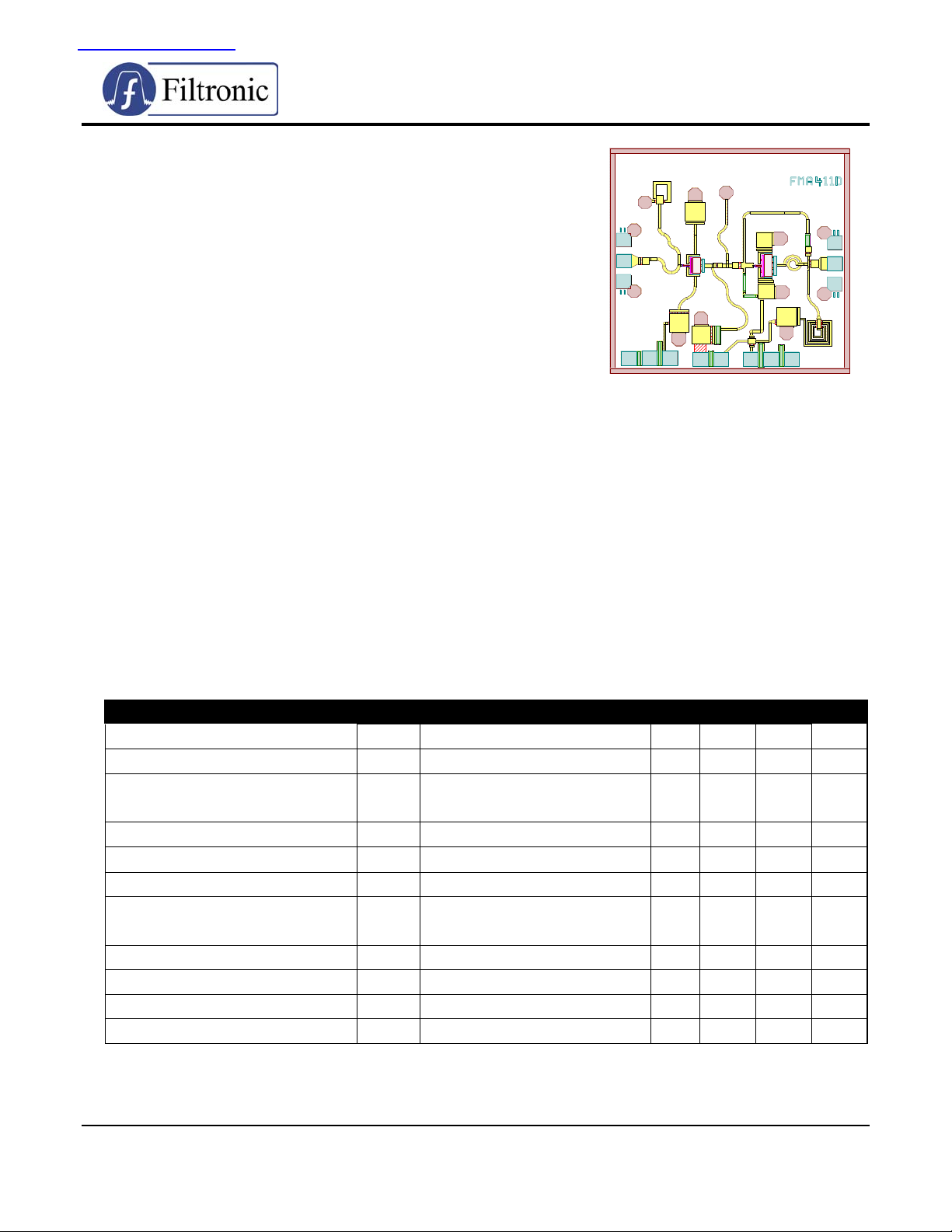
LOW-NOISE X-BAND MMIC
FMA411
• PERFORMANCE
♦ 8.5 – 14.0 GHz Operating Bandwidth
♦ 2.6 dB Noise Figure
♦ 18 dB Small-Signal Gain
♦ 17.5 dm Output Power
♦ +6V Single Bias Supply
♦ Adjustable Operating Current
♦ DC De-coupled Input and Output Ports
• DESCRIPTION AND APPLICATIONS
The FMA411 is a 2-stage, reactively matched pHEMT low-noise MMIC amplifier designed for use
over the 8.5 to 14.0 GHz bandwidth. The amplifier requires a single +6V supply and one off-chip
component for supply de-coupling; the supply voltage can be varied from +3V to +6V if needed.
Both the input and output ports are DC de-coupled. Grounding of the amplifier is provided by plated
thru-vias to the bottom of the die, no additional ground is required. Operating current can be
adjusted using the Source resistor ladders located along the bottom edge, by bonding a particular pad
to ground, in order to optimize noise or power performance.
Typical applications include low-noise front end amplifiers, and general gain block utilizations in Xband. The amplifier is unconditionally stable over all load states (-45 to +85°C), and conditionally
stable if the input port is open-circuited.
• ELECTRICAL SPECIFICATIONS AT 22°C
Parameter Symbol Test Conditions Min Typ Max Units
Operating Frequency Bandwidth BW 8.5 14 GHz
Small Signal Gain S21 V
Saturated Drain Current
I
V
DSS
(see Note)
Operating Current IDQ V
Small Signal Gain Flatness
∆S
21
Noise Figure NF V
3rd-Order Intermodulation Distortion IMD V
Power at 1dB Compression P
V
1dB
Input Return Loss S11 V
Output Return Loss S22 V
Reverse Isolation S
12
DD
V
DD
DD
DD
DD
DD
DD
V
DD
= +6 V I
= +3V 210 230 270 mA
DD
= +6V 125 140 165 mA
DD
= +6 V I
= +6 V I
= +6 V I
P
= +6 dBm SCL
OUT
= +6 V I
= +6 V I
= +6 V I
= +6 V I
≈ 60% I
DD
≈ 60% I
DD
≈ 60% I
DD
≈ 60% I
DD
≈ 60% I
DD
≈ 60% I
DD
≈ 60% I
DD
≈ 60% I
DD
16.5 18 21 dB
DSS
DSS
DSS
DSS
2.6 3.5 dB
± 0.8 ± 1.2
-46
16 17.5 dBm
DSS
DSS
-16 -10 dB
DSS
-40 -35 dB
DSS
-10 -6 dB
dB
dBc
• NOTE: Continuous operation at I
Phone: +1 408 850-5790 www.filcs.com Revised: 7/19/04
Fax: +1 408 850-5766 Email: sales@filcsi.com
is not recommended
DSS
PRELIMINARY
FMA411
LOW-NOISE X-BAND MMIC
ABSOLUTE MAXIMUM RATINGS1
Parameter Symbol Test Conditions Min Max Units
Supply Voltage V
Supply Current I
RF Input Power P
Storage Temperature T
Total Power Dissipation P
DD
DD
IN
STG
TOT
Gain Compression Comp. Under any bias conditions 5 dB
Simultaneous Combination of Limits2
1
T
= 22°C unless otherwise noted
Ambient
2
Users should avoid exceeding 80% of 2 or more Limits simultaneously
Notes:
• Operating conditions that exceed the Absolute Maximum Ratings will result in permanent damage to the device.
• Total Power Dissipation defined as: P
P
DC
P
IN
P
OUT
≡ (PDC + PIN) – P
TOT
: DC Bias Power
: RF Input Power
: RF Output Power
• Total Power Dissipation to be de-rated as follows above 22°C:
P
= 0.6 - (0.004W/°C) x T
TOT
where T
= carrier or heatsink temperature above 22°C
CARRIER
(coefficient of de-rating formula is the Thermal Conductivity)
Example: For a 55°C carrier temperature: P
= 0.6 - (0.004 x (55 – 22)) = 0.47W
TOT
• For optimum heatsinking eutectic die attach is recommended; conductive epoxy die attach is acceptable with
some degradation in thermal de-rating performance (P
• Note on Thermal Resistivity: The nominal value of 250°C/W is stated for the input stage, which will reach
temperature limits before the output stage. The aggregate MMIC thermal resistivity is approximately 175°C/W.
For any operating current 8 V
For VDD < 7V 75% I
mA
DSS
For standard bias conditions 0 dBm
Non-Operating Storage -40 150 ºC
See De-Rating Note below 980 mW
2 or more Max. Limits 80 %
, where:
OUT
CARRIER
= 550mW)
TOT
• HANDLING PRECAUTIONS
To avoid damage to the devices care should be exercised during handling. Proper Electrostatic
Discharge (ESD) precautions should be observed at all stages of storage, handling, assembly, and
testing. These devices should be treated as Class 1A per ESD-STM5.1-1998, Human Body Model.
Further information on ESD control measures can be found in MIL-STD-1686 and MIL-HDBK-263.
Phone: +1 408 850-5790 www.filcs.com Revised: 7/19/04
Fax: +1 408 850-5766 Email: sales@filcsi.com
 Loading...