

Page 1

FIC CONFIDENTIAL AND PROPRIETARY
MB02 Functional Specifications Rev. 0.3 Page 1
Notebook Personal Computer
< MB02>
Functional Specifications
Revision 0.3 Date: 01/20 ’03
ALL CONTENT ARE SUBJECT TO CHANGE
FIC Ltd
Hardware department
Manager: Joe Chen
Supervisor: Eric Yang
Written By: Steven Hsu
FIC H/W
FIC CONFIDENTIAL AND PROPRIETARY 11-November-2002_
PDF created with FinePrint pdfFactory trial version http://www.fineprint.com
Page 2

FIC CONFIDENTIAL AND PROPRIETARY
MB02 Functional Specifications Rev. 0.3 Page 2
All rights reserved by FIC Corporation. This document must be used solely for the
purpose for which it was furnished by FIC Corporation. No part of this document may be
reproduced or disclosed to others, in any form, without the prior written permission of
FIC Corporation.
Reference <T.B.D>
1. <MB02> Power Management Sub System Functional Specifications
2. <PMU08> Power Management Unit Functional Specifications
3. MB02 Key Component List
FIC H/W
FIC CONFIDENTIAL AND PROPRIETARY 11-November-2002_
PDF created with FinePrint pdfFactory trial version http://www.fineprint.com
Page 3

FIC CONFIDENTIAL AND PROPRIETARY
MB02 Functional Specifications Rev. 0.3 Page 3
Revision History
Revision Date Description Sections
FIC H/W
FIC CONFIDENTIAL AND PROPRIETARY 11-November-2002_
PDF created with FinePrint pdfFactory trial version http://www.fineprint.com
Page 4

FIC CONFIDENTIAL AND PROPRIETARY
MB02 Functional Specifications Rev. 0.3 Page 4
TABLE OF CONTENTS
1. OVERVIEW…………………………………………………………………………………………6
1 Overview.................................................................................................................................................7
1.1 FEATURES................................................................................................................................................7
1.2 MODELS ................................................................................................................................................11
2 Specifications........................................................................................................................................12
2.1 BLOCK DIAGRAM..................................................................................................................................12
2.2 HARDWARE SPECIFICATIONS ...............................................................................................................13
2.2.1 Device Specifications.............................................................................................................13
2.2.2 I/O Interface Specification.....................................................................................................16
2.2.3 I/O Port & Slot Specifications ...............................................................................................17
2.2.4 Key Components....................................................................................................................18
2.2.5 Size and Weight .....................................................................................................................19
2.2.6 Battery Handling(TBD) .........................................................................................................19
3 Parts List ..............................................................................................................................................20
4 User Interfaces.....................................................................................................................................21
4.1 SWITCHES..............................................................................................................................................21
4.2 HOT KEY FUNCTION............................................................................................................................23
4.2.1 International model................................................................................................................23
4.3 AUDIO DJ FUNCTION(NONE) ...............................................................................................................24
4.4 LED’S....................................................................................................................................................24
4.4.1 Power Status LED Indicator (1 LED’s)..................................................................................24
4.4.2 Keyboard Lock LED Indicator (3 LED’s)..............................................................................24
4.4.3 1
4.4.4 PHS Accessible area / Mail receive LED Indicator (1 LED) (NO SUPPORT) .....................24
4.4.5 BlueTooth/Wireless Access LED Indicator (1 LED) .............................................................24
4.4.6 HDD Status LED Indicator (1 LED’s)...................................................................................25
4.4.7 LED Setting ...........................................................................................................................26
4.5 POWER MANAGEMENT SUPPORT ACPI.............................................................................................27
4.6 BUZZER STATUS (NOT SUPPORT)..........................................................................................................27
5 Memory ................................................................................................................................................28
5.1 MEMORY MAP ......................................................................................................................................28
5.2 SYSTEM MEMORY (DDR SDRAM) .....................................................................................................29
5.3 HOW TO ACCESS SPD............................................................................................................................30
5.4 ABOUT THE SUPPORT OF PC-200 AND PC-266.....................................................................................31
5.5 BIOS .....................................................................................................................................................31
6 PCI........................................................................................................................................................33
6.1 INTERFACE SPECIFICATIONS................................................................................................................33
6.2 PCI AGENTS..........................................................................................................................................33
6.3 PCI MASTER DEVICES .........................................................................................................................35
6.4 PCI CONFIGURATION ...........................................................................................................................35
6.5 INTEL MONTARA-GM GMCH REGISTERS SUMMARY(DEVICE 0, FUNCTION 0)...............................36
6.6 INTEL MONTARA-GM MAIN MEMORY CONTROL REGISTERS SUMMARY(DEVICE 0, FUNCTION 1) 36
6.7 INTEL MONTARA-GM GMCH CONFIGURATION PROCESS REGISTERS SUMMARY(DEVICE 0,
FUNCTION 3) .................................................................................................................................................37
st
Battery Status LED Indicator (1 LED)..............................................................................24
FIC H/W
FIC CONFIDENTIAL AND PROPRIETARY 11-November-2002_
PDF created with FinePrint pdfFactory trial version http://www.fineprint.com
Page 5

FIC CONFIDENTIAL AND PROPRIETARY
MB02 Functional Specifications Rev. 0.3 Page 5
6.8 INTEL MONTARA-GM GMCH INTEGRATED GRAPHIC REGISTERS SUMMARY(DEVICE 2, FUNCTION
0) 37
6.9 INTEL ICH4-M LAN CONTROLLER REGISTERS SUMMARY(BUS 1, DEVICE 8, FUNCTION 0)...........38
6.10 INTEL ICH4-M HUB INTERFACE TO PCI BRIDGE REGISTERS SUMMARY(DEVICE 30, FUNCTION 0)39
6.11 ICH4-M LPC(DEVICE 31:FUNCTION 0) REGISTER...................................................................40
6.12 ICH4-M RTC REGISTERS...............................................................................................................41
6.13 INTEL ICH4-M POWER MANAGEMENT REGISTERS SUMMARY(DEVICE 31, FUNCTION 0) ..............42
6.14 ICH4-M ACPI CONFIGURATION REGISTERS.............................................................................42
6.15 ICH4-M SYSTEM MANAGEMENT TCO REGISTERS..................................................................43
6.16 CH4-M GENERAL PURPOSE IO CONFIGURATION REGISTERS ...............................................43
6.17 ICH4-M IDE CONFIGURATION SPACE(DEVICE 31:FUNCTION 1) REGISTER.......................44
6.17.1 IDE Interface .........................................................................................................................44
6.17.2 PCI Bus Master IDE I/O Register..........................................................................................45
6.18 ICH4-M USB CONTROLLERS CONFIGURATION REGISTERS(DEVICE 29:FUNCTION 0,1,2)45
6.19 ICH4-M USB I/O REGISTER..............................................................................................................46
6.20 ICH4-M USB EHCI COTROLLER REGISTER (DEVICE 29:FUNCTION 7)..............................46
6.21 ICH4-M USB ENHANCED HOST CONTROLLER CAPABILITY REGISTER..........................................47
6.22 ICH4-M USB ENHANCED HOST CONTROLLER OPERATIONAL REGISTER......................................47
6.23 ICH4-M SMBUS COTROLLER REGISTER (DEVICE 31:FUNCTION 3)....................................48
6.24 ICH4-M SMBUS IO REGISTER..........................................................................................................49
6.25 CH4-M AC97 AUDIO COTROLLER REGISTER (DEVICE 31:FUNCTION 5)............................49
6.26 ICH4-M NATIVE AUDIO BUS MASTER CONTROL IO REGISTER ......................................................50
6.27 CH4-M AC97 MODEM COTROLLER REGISTER (DEVICE 31:FUNCTION 6).........................51
6.28 ICH4-M AC97 MODEM IO REGISTER ..............................................................................................52
6.29 ICH4-M MODEM IO REGISTER.........................................................................................................52
7 I/O CONFIGURATIONS....................................................................................................................53
7.1 ISA REGISTERS TABLES .......................................................................................................................53
7.2 INTERRUPT ASSIGNMENTS....................................................................................................................55
7.3 I/O MAP ...............................................................................................................................................56
7.4 KEYBOARD CONTROLLER....................................................................................................................58
7.4.1 Mouse INT Mask(IRQ12 Mask)............................................................................................59
7.5 SMBUS I/F ............................................................................................................................................60
7.5.1 SMBus1 Block Diagram........................................................................................................60
7.5.2 SMBus1 Connection Device Address....................................................................................60
7.5.3 SMBus2 Block Diagram........................................................................................................60
7.5.4 SMBus2 Connectin Device Address......................................................................................61
7.6 CLOCK CONTROL..................................................................................................................................62
7.6.1 Clock synthesizer/driver ........................................................................................................62
8 SYSTEM MANAGEMENT................................................................................................................65
8.1 GPIO SET REGISTER LIST ....................................................................................................................65
8.1.1 Intel ICH4-M GPIO Configuration........................................................................................65
8.1.2 PMU08 GPIO Configuration.................................................................................................65
8.2 SYSTEM MANAGEMENT GPIO.............................................................................................................66
8.2.1 ICH4-M GPIOs allocation.....................................................................................................66
8.2.2 PMU08 GPIOs allocation......................................................................................................67
8.2.3 LPC KBC M38859 GPIOs allocation....................................................................................69
9 PCMCIA/CardBus Controller............................................................................................................70
10 Video Controller ..................................................................................................................................71
FIC H/W
FIC CONFIDENTIAL AND PROPRIETARY 11-November-2002_
PDF created with FinePrint pdfFactory trial version http://www.fineprint.com
Page 6

FIC CONFIDENTIAL AND PROPRIETARY
MB02 Functional Specifications Rev. 0.3 Page 6
11 Sound....................................................................................................................................................74
12 MODEM...............................................................................................................................................75
13 SWITCH SETTING TABLE AND PANEL ID..................................................................................76
13.1 DSW1(ON DD BOARD) SWITCH SETTING TABLE.........................................................................76
Keyboard Type Select............................................................................................................................76
DSW1 76
1 76
2 76
US KEYBOARD..............................................................................................................................................76
OFF 76
OFF 76
RESERVE 76
OFF 76
ON 76
JP KEYBOARD...............................................................................................................................................76
ON 76
OFF 76
UK KEYBOARD .............................................................................................................................................77
ON 77
ON 77
BIOS Crisis Select.................................................................................................................................77
13.2 SW1(BESIDE THE GLIDE PAD CONNECTOR) SWITCH SETTING TABLE....錯誤! 尚未定義書籤。
CD-ROM Cable Select ..........................................................................................................................77
CMOS Clear Select................................................................................................................................77
13.3 PANEL ID SETTING...........................................................................................................................77
14 PC 2001 Checklist................................................................................................................................78
BASIC PC 2001..............................................................................................................................................78
MOBILE PC 2001 ..........................................................................................................................................81
15 POWER SEQUENCE TIMING.........................................................................................................83
15.1 BATTERY ONLY POWER ON..........................................................................................................83
15.2 ADAPTER ONLY POWER ON (FIRST TIME)....................................................................................85
15.3 S4 OR S5 POWER ON.........................................................................................................................87
VRON_VCCP ...................................................................................................................................................88
VCCP/1.2VDDM.................................................................................................................................................88
15.4 S3 SUSPEND AND RESUME.............................................................................................................89
15.5 S4 SUSPEND AND RESUME.............................................................................................................91
15.6 S4 OR S5 POWER OFF.......................................................................................................................93
FIC H/W
FIC CONFIDENTIAL AND PROPRIETARY 11-November-2002_
PDF created with FinePrint pdfFactory trial version http://www.fineprint.com
Page 7

FIC CONFIDENTIAL AND PROPRIETARY
MB02 Functional Specifications Rev. 0.3 Page 7
1 Overview
1.1 Features
Notebook size, 2 spindle, IBM PC/AT compatible personal computer with PCI-bus and
Multimedia functions , provide full basic function with lowest price and easy of use.
The following is a summary of MB02 features:
CPU
CPU Type uFCPGA 479pin
Intel Banias 1.3/1.4/1.5/1.6/1.7 GHZ
TDP(Target) 24.5W
Chip Set
Core Logic Intel Montara-GM (North) :CPU(Banias) I/F, LVDS I/F, RGB analog I/F
200/266 DDR MEMORY I/F, Hub-Link I/F,
DVOB&DVOC IF….
Intel ICH4-M (South) : PCI I/F, LPC I/F, ATA100 IDE I/F, Hub-Link
I/F ,AC97 V2.2 I/F, RTC, 2.0/1.1USB I/F, 10/100M
LAN I/F, GPIO, ACPI, APIC….
Memory
Support Memory DDR266/200 SDRAM 128/256/512MB/1G SO-DIMM
Memory Slots 2 Slots SO-DIMM (1.25”)
Max Memory 2GB (1GB per DIMM )
Video
Controller Embedded in Intel Montara-GM.
UMA (using DVMT configuration)
High performance & High quality 3D accelerator
High performance 2D accelerator
Complete TV-OUT/Digital flat panel solution
MPEG-2/1 video decoder
Video accelerator
LCD Panel 14.1” XGA
Controlled by hot key (8 level)
FIC H/W
FIC CONFIDENTIAL AND PROPRIETARY 11-November-2002_
PDF created with FinePrint pdfFactory trial version http://www.fineprint.com
Page 8

FIC CONFIDENTIAL AND PROPRIETARY
MB02 Functional Specifications Rev. 0.3 Page 8
PCMCIA
Controller RICOH R5C551 Single Slot PCI-CARDBUS BRIDGE
Built in Smart Card reader(None)
ZV-Port Support (None)
Ring wakeup support(None)
Power Switch TPS2211A(TI)
Sound
Controller Integrated in Intel ICH4-M (PCI audio)
CODEC Realtek ALC202 AC97 CODEC 2.2 S/PDIF
Function Sound Blaster Compatible
S/W Wave Table
Buzzer Support (None)
Volume SW control.
IEEE 1394(Option) Support one port
Controller RICOH R5C551 two IEEE1394 ports BRIDGE
Function Compliant with Link Layer Services as defined in 1394 Open Host
Compliant with Physical Layer Services as defined in P1394a draft
Storage
USB FDD 3.5” 3 mode(option)
IDE bus IDE bus
Bus Mastering
Ultra DMA 33/66/100
PIO mode 0,1,2,3,4
Internal HDD 2.5” 9.5 mmH Pack
Internal Optical Drive
DVD Combo 8x DVD , 8x CDR, CDRW write , 20x CD-ROM 9.5mm type (KME:
Controller Interface specification release 1.0
2.0(Data Rate 100/200/400 Mbps)
UJDA745, Toshiba: SD-R9022)
Communication
Internal Modem ASKEY (1456VQL19V) (MDC Modem AC97 Interface) (Option)
FIC H/W
FIC CONFIDENTIAL AND PROPRIETARY 11-November-2002_
PDF created with FinePrint pdfFactory trial version http://www.fineprint.com
Page 9

FIC CONFIDENTIAL AND PROPRIETARY
MB02 Functional Specifications Rev. 0.3 Page 9
V.90, K56flex
RJ11 Jack
Wake up on Ring support S1 or S3
Voice Function not support
Internal Bluetooth/Modem Combo
ActionTec (MBC) (MDC Modem AC97 Interface / USB) (Option)
MDC Modem:
V.90, K56flex
RJ11 Jack
Wake up on Ring support S1 or S3
Voice Function not support
Bluetooth:
2.4GHz~2.4835GHz
CSR solution
Support Coexistence function.
Internal LAN Intel ICH4-M + Intel 82562EZ
10Base-T/100Base-TX
RJ-45 jack
Internal LAN Intel 82541EI (PCI device) (Option)
Giga Lan solution
RJ-45 jack
I/O
Serial port Not support
Parallel port Not support
CRT D-sub 15pin x1
USB 4pin x3 port
IEEE 1394 one port
H/P Min Jack x1
Mic In Min Jack x1
PDC/PIAFS Special 24pin cancel (support by USB)
Modem RJ11 x1
LAN RJ45 x1
Docking Not support
IR Not support
FIC H/W
FIC CONFIDENTIAL AND PROPRIETARY 11-November-2002_
PDF created with FinePrint pdfFactory trial version http://www.fineprint.com
Page 10

FIC CONFIDENTIAL AND PROPRIETARY
MB02 Functional Specifications Rev. 0.3 Page 10
Versa Bay III Not support
Keyboard
Pitch/Travel 19mm/3mm
Language US, Japan, French, UK, Italian, Spanish, Germany, Belgian
Norwegian, Danish, Swedish, Portuguese, T.Chinless, Korean
Tbits
Hot Key Fn+F2: Wireless On/Off
Fn+F3: Display Mode
Fn+F4: Sleep
Fn+F6: Speaker On/Off
Fn+F8: Brightness Up (8 level)
Fn+F9: Brightness Down (8 level)
Fn+F12: Scroll Lock
Fn+ArrowR: Sound up
Fn+ArrowL: Sound down
Point Device SYNAPTICS TM41PDG351-1 Glide Pad
AC Adapter LITEON PA-1600-05
Input AC 100-240V
Output 19V, 60W Peak80W
Color Black or White
Battery
1st battery Li-ion (8 cell) :Pansonic 52Wh
Battery Life Under ACPI
RTC battery x1
Bridge battery Not support
Switch
Power SW Push button type (As asserted switch over 4s,system will be powered
down by force )
Short Cut Key User define button x2 , define by user
( Internet button , support power on from S1/S4/S5
E-Mail button , support power on from S1/S4/S5 )
LED
Power Status Yes (Need see while LCD is closed)
FIC H/W
FIC CONFIDENTIAL AND PROPRIETARY 11-November-2002_
PDF created with FinePrint pdfFactory trial version http://www.fineprint.com
Page 11

FIC CONFIDENTIAL AND PROPRIETARY
MB02 Functional Specifications Rev. 0.3 Page 11
Battery Charge Yes (Need see while LCD is closed)
IDE Device Access Yes (HDD & CD-ROM )
FDD Access No
Caps Lock Yes
Scr Lock Yes
Num Lock Yes
Mail arrival No
RF Access Yes
Security
Kensington Lock Hole x1
PMU PMU08
Compliance
PC2001 compliant
ACPI compliant
Plug and Play Support
Auto Configuration
16bit I/O Address Decoded
Selectable I/O Address, IRQ and DMA
1.2 Models
Please refer to the Notebook PC Development Plan Document in detail.
FIC H/W
FIC CONFIDENTIAL AND PROPRIETARY 11-November-2002_
PDF created with FinePrint pdfFactory trial version http://www.fineprint.com
Page 12
Mob
ile 1.3~/1.7
GHZ
ROM
Mini PCI
Speaker
ALC20
2
Tooth
FIC CONFIDENTIAL AND PROPRIETARY
MB02 Functional Specifications Rev. 0.3 Page 12
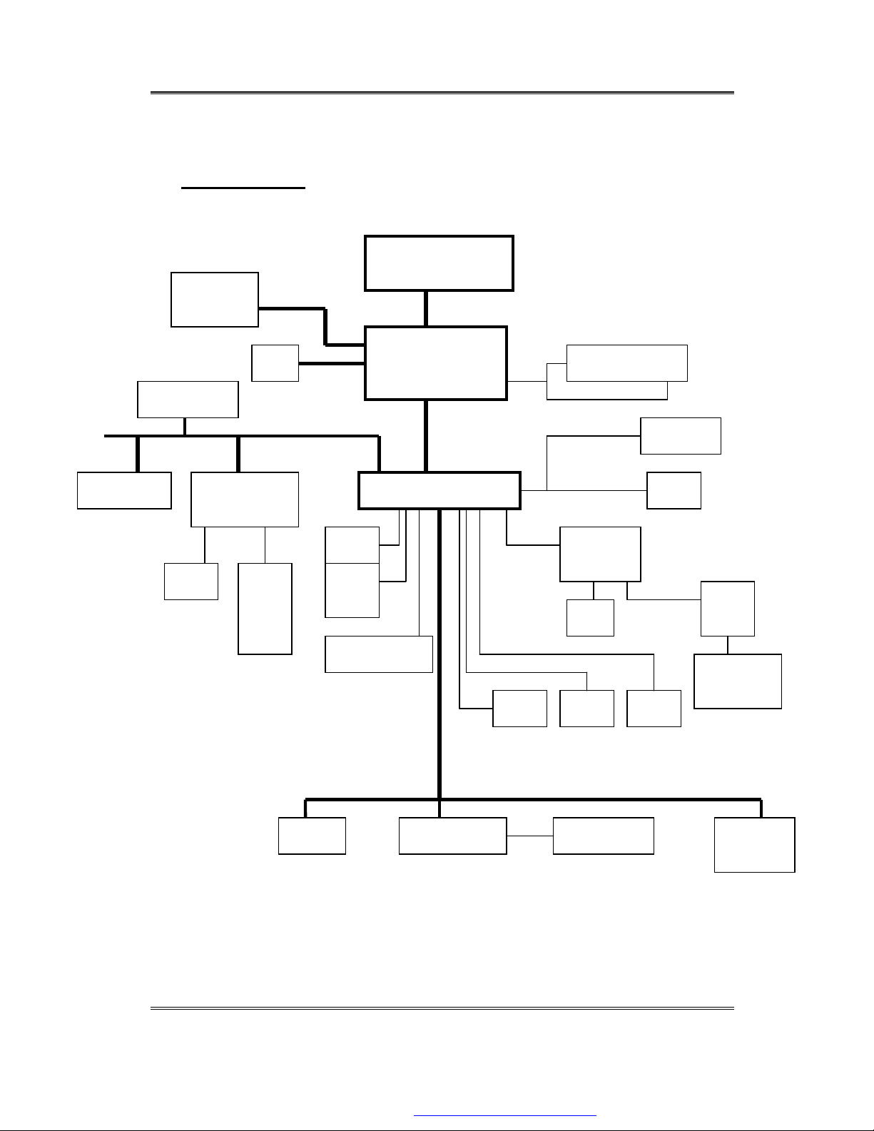
2 Specifications
2.1 Block Diagram
LCD
Intel 82541EI
1394
LVDS Interface
CRT
PCI BUS
RICOH
R5C551
Slot1
PMU08
Intel uFCPGA Banias
North Bridge
Intel MGM
Intel ICH4
MDC
Blue
Intel 82562EZ
LPC Interface
GTL_BUS
Hub-Link
KBC M3885X
USB 0
DDR SDRAM
DDR SDRAM
IDE
CODEC
MIC
USB 1
KB/Glide pad
CD-ROM
HDD
Amp
Headphone
USB 2
Flash
FIC H/W
FIC CONFIDENTIAL AND PROPRIETARY 11-November-2002_
PDF created with FinePrint pdfFactory trial version http://www.fineprint.com
Page 13

FIC CONFIDENTIAL AND PROPRIETARY
MB02 Functional Specifications Rev. 0.3 Page 13
2.2 Hardware Specifications
2.2.1 Device Specifications
Category Specification Stepping
CPU Intel Processor uFCPGA 479pin
Intel Banias 1.3/1.4/1.5/1.6/1.7 GHZ
(BUS: 100MHz)
Core Logic
Cache Memory L1 Cache (Pentium Processor internal):
L2 Cache (Pentium Processor internal):
System Memory Expansion Memory: 2 SO-DIMM Slot (1.25”)
BIOS ROM Flash ROM
Intel Montara-GM (North Bridge) :
CPU(Banias) I/F
VGA Controller
LVDS I/F
DVOB&DVOC IF.
RGB analog I/F
200/266 DDR MEMORY I/F
Hub-Link I/F
Intel ICH4-M (South Bridge) :
Integrated Hub-Link I/F to connect with PCI Bridge
Dual IDE Master/Slave Controller ,Integrated DMA Controller
1.1/2.0 Universal Serial Bus Host Controller
Integrated 10/100M Fast Ethernet MAC Controller
Integrated Audio Controller with AC97 V2.2 Interface
Advanced Power Management(ACPI)
RTC
Integrated PCI to LPC Bridge
Integrated Audio Controller with AC97 Interface
PCI Bus Interface (PCI 2.2 compliant)
GPIO
Advance PIC
12KB code and 8KB data
8-way cache associativity provides
256KB Advanced Transfer Cache,8 way associativity
8-way set associative, 32-byte line size, 1 line per sector
Size: 128/256/512MB/1G
Type: DDR DRAM, 3.3V
Data Path: 64Bit
Frequency : 266/200MHz
Please refer to the MB02 Key component list in detail.
1st Vendor : SST 49LF004A TSSOP Package 4Mbit LPC flash ROM
2nd Vendor : <TBD>
4Mbit, 32 pin TSSOP package
PS: PLCC32 Package is just for DEBUG
FIC H/W
FIC CONFIDENTIAL AND PROPRIETARY 11-November-2002_
PDF created with FinePrint pdfFactory trial version http://www.fineprint.com
Page 14

FIC CONFIDENTIAL AND PROPRIETARY
MB02 Functional Specifications Rev. 0.3 Page 14
Super I/O
RTC + NVRAM Integrated in South Bridge (Intel ICH4-M)
K/B Controller Mitsubishi M38859 LPC KBC
PMU New PMU08
VGA Controller Embedded in Intel Montara-GM
VRAM Share system memory, UMA (using DVMT configuration)
None
Real Time Clock with 256 byte extended CMOS.
IBM AT Clock/Calendar/Alarm (14 Bytes)
Internal K/B, Touch Pad, External K/B or M/S
Supported A20Gate,firmware version 2.14
Mitsubishi M38859FFHP
Embedded Controller
High Performance and high quality 3D accelerator
Integrated dual DVO bridge
Integrated LVDS Interface
Integrated RGB analog Interface
High performance 2D accelerator
Complete TV-OUT/Digital Flat Panel Solution
TV out encoder None
LVDS Transmitter None
CardBus Controller
Sound
Modem Askey / Actiontec MDC modem
On board LAN Intel ICH4-M + Intel 82562EZ
RICOH R5C551 (PCI Card Bus controller)
PC/Card Bus Type II x1
Build in smart card (none)
AC’97 CODEC
Realtek ALC202
AC’97 Revision 2.2 Compliant
V.90, K56flex, ITU-T V.34, V.32, RJ11 Jack
TIA/EIA 602, V.42
ITU-T V.17, V.29, V.27ter, V.21 Ch2
TIA/EIA 578 Class1 FAX
Wake up on Ring
Support LAN boot
Support for auto-negotiation (10BASE-T and 100BASE-TX)
Wake up On LAN
Intel 82541EI Giga LAN (Option)
FIC H/W
FIC CONFIDENTIAL AND PROPRIETARY 11-November-2002_
PDF created with FinePrint pdfFactory trial version http://www.fineprint.com
Page 15

FIC CONFIDENTIAL AND PROPRIETARY
MB02 Functional Specifications Rev. 0.3 Page 15
802.11b Support by Intel Calexico Mini-PCI Wireless LAN Card
<Design Ready Only>
1394 RICOH R5C551, support one port
Cellular I/F Support PDC/PIAFS/CdmaOne/Dupa(None) Support by
USB
Intel ICH4-M)
Integrated in South Bridge Intel ICH4-M)
USB v.1.1 and Intel Universal HCI v.1.1 compatible
USB v.2.0 and Enhance Universal HCI v.2.0 compatible
Eighteen level (doublewords) data FIFO with full scatter and gather
capability
Root hub and four function ports
Integrated physical layer transceivers with optional over-current
detection status on USB inputs
Cellular I/F
USB Cable
FIC H/W
FIC CONFIDENTIAL AND PROPRIETARY 11-November-2002_
PDF created with FinePrint pdfFactory trial version http://www.fineprint.com
Page 16

FIC CONFIDENTIAL AND PROPRIETARY
MB02 Functional Specifications Rev. 0.3 Page 16
2.2.2 I/O Interface Specification
Category Specification Remark
IDE Interface
(Intel ICH4-M)
Printer Interface
Serial Interface
External PS/2 Port
(M38859)
Universal Serial Bus
(Intel ICH4-M)
Infrared
Modem
LAN
Fast IDE, 2 ports:
--Integrated multithreaded I/O link mastering with read pipelined
streaming
--Dual independent IDE channel each with 16 DW FIFO
--Native and compatibility mode
--PIO mode 0,1,2,3,4, and multiword DMA mode 0,1,2
--Ultra DMA 33/66/100
None
None
External Keyboard or PS/2 Mouse
Exclusively connected.
Can use both device by using branch cable(option)
--Integrated multithreaded IO link mastering
--Dual independent OHCI controllers with root hub
--Support up to 6 USB ports
--Support legacy devices
--Over current detection equipped
--Option to separately configure each port as a wake-up source
None
56K Data/Fax Modem (v.90)
10/100 Base TX LAN
Lan boot support and WFM 2.0
FIC H/W
FIC CONFIDENTIAL AND PROPRIETARY 11-November-2002_
PDF created with FinePrint pdfFactory trial version http://www.fineprint.com
Page 17

FIC CONFIDENTIAL AND PROPRIETARY
MB02 Functional Specifications Rev. 0.3 Page 17
2.2.3 I/O Port & Slot Specifications
Category Specification Remark
Serial port
Parallel port
VGA CRT port
USB port
Port Bar
Headphone
Line In
Mic In
DC In
TV out
LAN,
Modem I/F
IEEE 1394
Docking
DIMM Memory Slot 1.25” SODIMM Slot x 2 Slot
Card Bus Slot Type II x1
Versa Bay III Not support
Internal HDD 1 Slot for 9.5mmH HDD
Battery Slot 1 Slot: Battery Core Pack
Not support
Not support
1 port (D-Sub 15 pin)
3 port: Base connector
Not support
1 Jack (Mono Mini Pin Jack 3P)
Not support
1 Jack (Mono Mini Pin Jack 3P)
1 port
Not support
1 port
1 port
1 port
Not support
Support 5V or 3.3V Card
Maximum power supply: 1 A(5V) or 1A(3.3V)
FIC H/W
FIC CONFIDENTIAL AND PROPRIETARY 11-November-2002_
PDF created with FinePrint pdfFactory trial version http://www.fineprint.com
Page 18

FIC CONFIDENTIAL AND PROPRIETARY
MB02 Functional Specifications Rev. 0.3 Page 18
2.2.4 Key Components
Category Specification Remark
LCD Panel 14.1” XGA
; Please refer to the MB02 Key component list in detail.
HDD 2.5 inch HDD (Standard)
9.5mm Height
; Please refer to the MB02 Key component list in detail.
CD-ROM
FDD(None)
DVD
CD-RW,Combo 9.5mm Height ,24X
Pointing Device Internal Touch Pad
Keyboard Internal Keyboard
Speakers (audio) Two built-in dynamic speakers
Microphone Built-in non-directional Back Electric Condenser
Buzzer Not support
Battery Battery Pack
RTC Battery Ni-MH Battery
DC/DC Converter Daughter board
CPU Vcore 1.3V Max 32A
CD-ROM (9.5mm Height)
; Please refer to the MB02 Key component list in detail.
USB FDD
3 mode Support
; Please refer to the MB02 Key component list in detail.
DVD
9.5mm Height ,8X
; Please refer to the MB02 Key component list in detail.
; Please refer to the MB02 Key component list in detail.
Pad SYNAPTICS : TM41P-351
Please refer to the MB02 Key component list in detail.
6.5mm Height, 3.0mm Stroke, 19mm Pitch
Vendor: ALLTOP
PAN-international
; Please refer to the MB02 Key component list in detail.
40 x 20mm, 1W 4Ω
Microphone
Panasonic : WM62PCX
Type: 8 cell Li-ION Battery with EEPROM
Voltage: 14.4V
Cell: 1800mAh Prisamtic
Method: 4P2S
Capacity: 3600mAh/52Wh Panasonic
Vendor: SANYO/ Panasonic
; Please refer to the MB02 Key component list in detail.
Model: 3/V 15H
Voltage: 3.6V
Capacity: 15mAh
Vendor: VARTA
5.0 V Max 7.0 A
3.3 V Max 4.5 A
1.5V Max 2A
1.8V Max1A
.
FIC H/W
FIC CONFIDENTIAL AND PROPRIETARY 11-November-2002_
PDF created with FinePrint pdfFactory trial version http://www.fineprint.com
Page 19

FIC CONFIDENTIAL AND PROPRIETARY
MB02 Functional Specifications Rev. 0.3 Page 19
AC Adapter PA-1600-05 : Liteon
Input: AC100 – 240V, 50/60Hz
Output: 19V, 60W Peak 80W
Size: 110mm x 50mm x 29mm (Liteon)
Vendor: Liteon
Color : TBD
; Please refer to the MB02 Key component list in detail.
2.2.5 Size and Weight
Category
Size 310MM X 266MM X 27.3 MM (H)
SUPPORTS KENSINGTON LOCK
Weight AROUND 2.54 KG OR 4.5 LBS WITH 14.1” LCD SYSTEM WITH HDD, FDD, CD-
ROM AND ONE LI-ION BATTERY PACK
2.2.6 Battery Handling(TBD)
Category
Battery Charging
Max Change Current:
1.7A-1.75A±150mA
Battery Life 1st Li-ion 4.5 h TBD
Remark
Power On Li-ion 3.5 h
Power Off Li-ion 3.5 h
Specification Remark
TBD
Save to RAM 1st Li-ion 3 Days TBD
Consumption power
Charge 24 h CMOS Battery
Discharge 3 month
Maximum 75W
Typical 25W TBD
MobileMark 10W Target
System on
System off
FIC H/W
FIC CONFIDENTIAL AND PROPRIETARY 11-November-2002_
PDF created with FinePrint pdfFactory trial version http://www.fineprint.com
Page 20

FIC CONFIDENTIAL AND PROPRIETARY
MB02 Functional Specifications Rev. 0.3 Page 20
3 Parts List
Refer to section 2.2 Hardware Specifications for major components.
FIC H/W
FIC CONFIDENTIAL AND PROPRIETARY 11-November-2002_
PDF created with FinePrint pdfFactory trial version http://www.fineprint.com
Page 21

FIC CONFIDENTIAL AND PROPRIETARY
MB02 Functional Specifications Rev. 0.3 Page 21
4 User Interfaces
4.1 Switches
Switches Description Note
Power switch The button switch is located at the top of the system . This
switch provides the Power ON/OFF and Suspend/Resume
function.
4sec pow-off operation.
Internet switch The button switch is located at the top of the system . This
switch support Power on from S1/S4/S5.(Option)
Mail switch The button switch is located at the top of the system . This
switch support Power on from S1/S4/S5.(Option).
User define switch The button switch is located at the top of the system .
Dip Switch (DSW1) <Location : On DD Board>
Keyboard
Select1
Keyboard
Select2
BIOS Crisis Bit4 ON: Enable
DVDSEL
RTC Clear Bit6 ON : Clear CMOS
Bit1 Refer to the below table 1. K/B
Bit2 Refer to the below table 1. K/B
OFF: Normal
Bit5 ON : connect to GND
OFF : NC
OFF : Normal operation
controller
Port 60
*1
controller
Port 61
*1
ICH4M
GPIO34
*1:Please refer to the keyboard controller Mitsubishi M38859 datasheet
Table 1. Keyboard code Selection
The Keyboard code selection by DIP SW BIT <1,2> are the following table.
FIC H/W
FIC CONFIDENTIAL AND PROPRIETARY 11-November-2002_
PDF created with FinePrint pdfFactory trial version http://www.fineprint.com
Page 22

FIC CONFIDENTIAL AND PROPRIETARY
MB02 Functional Specifications Rev. 0.3 Page 22
Bit 1 ; logic Bit 2 ; logic Keyboard code Remark
OFF ; Hi OFF ; Hi US Keyboard
ON ; Low OFF ; Hi JP Keyboard
OFF ; Hi ON ; Low Reserved
ON ; Low ON ; Low UK Keyboard
FIC H/W
FIC CONFIDENTIAL AND PROPRIETARY 11-November-2002_
PDF created with FinePrint pdfFactory trial version http://www.fineprint.com
Page 23

FIC CONFIDENTIAL AND PROPRIETARY
MB02 Functional Specifications Rev. 0.3 Page 23
4.2 HOT Key Function
4.2.1 International model
Hot Key Function Description Note
Fn + F2 Wireless On/Off Open or close wireless function including of BT or
wireless LAN
Fn + F3 Display Toggles the Video Mode through LCD-only, CRT-
only, Simultaneous .
Fn + F4 Standby
Fn + F6 Speaker Volume Speaker ON/OFF
Fn + F8 Brightness Control Brightness Up (8 level)
Fn + F9 Brightness Control Brightness Down (8level)
Fn + F12 Scroll Control Scroll Lock
Fn + ArrowR Sound Amplifier Sound up
Fn + ArrowL Sound Amplifier Sound down
Standby power management mode. Press key to set
system in standby power management mode.
FIC H/W
FIC CONFIDENTIAL AND PROPRIETARY 11-November-2002_
PDF created with FinePrint pdfFactory trial version http://www.fineprint.com
Page 24

FIC CONFIDENTIAL AND PROPRIETARY
: On, * : Blink
MB02 Functional Specifications Rev. 0.3 Page 24
4.3 Audio DJ Function(None)
4.4 LED’s
4.4.1 Power Status LED Indicator (1 LED’s) (A&B of Panel)
: On, * : Blink
Status Under AC Under Battery
On Save to RAM
Normal Off Green * Green
Battery Low
Green * Green
Off On Save to RAM
N/A Beep * Beep
4.4.2 Keyboard Lock LED Indicator (3 LED’s) (B of Panel)
: On, * : Blink
Status Under AC Under Battery
On Save to RAM
Caps Lock Green Off Off Green Off Off
Scroll Lock Green Off Off Green Off Off
Num Lock Green Off Off Green Off Off
4.4.3 1
: On, * : Blink
Status Under AC Under Battery
On Save to RAM
1st Battery Charge Green Green Green N/A N/A N/A
1st Battery Error * Green * Green * Green N/A N/A N/A
Not Used/ Full /
Empty
st
Battery Status LED Indicator (1 LED) (B of Panel)
Off Off Off Off Off Off
Off On Save to RAM
Off On Save to RAM
4.4.4 PHS Accessible area / Mail receive LED Indicator (1 LED) (NO SUPPORT)
Off
Off
Off
Off
Status Under AC Under Battery
On S1 Off On S1 Off
Mail arrival/PHS(Not
support)
LOGO LED(Not
support)
Note : LOGO LED can disply 7 kinds color,the combination by Amber ,Green and Blue.
Green
/*
Amber
Green
Blue
Green(Mail)
/ *
Off Green
Off
/ *
Amber
Green
Blue
Green(Mail)
/ *
Off
Off
4.4.5 BlueTooth/Wireless Access LED Indicator (1 LED) (A&B of Panel)
FIC H/W
FIC CONFIDENTIAL AND PROPRIETARY 11-November-2002_
PDF created with FinePrint pdfFactory trial version http://www.fineprint.com
Page 25

FIC CONFIDENTIAL AND PROPRIETARY
: On, * : Blink
MB02 Functional Specifications Rev. 0.3 Page 25
Status Under AC Under Battery
On S1 Off On S1 Off
BlueTooth &
Wireless LAN
Power ON
BlueTooth &
Wireless LAN
Power OFF
Green Off Off Green Off Off
Off Off Off Off Off Off
4.4.6 HDD Status LED Indicator (1 LED’s) (B of Panel)
: On, * : Blink
Status Under AC Under Battery
On Save to RAM
Access * Green Off Off * Green Off Off
Off On Save to RAM
Off
FIC H/W
FIC CONFIDENTIAL AND PROPRIETARY 11-November-2002_
PDF created with FinePrint pdfFactory trial version http://www.fineprint.com
Page 26
FIC CONFIDENTIAL AND PROPRIETARY
7 6 5 4 3 2 1 0
E S
*1 R E S
*1 P O W _ L E D
MB02 Functional Specifications Rev. 0.3 Page 26
4.4.7 LED Setting
4.4.7.1 Power status LED
When shifting to Sleep state and suspend state, thing changed to the BIOS blink setting is necessary for
power status LED.
This setting is done by PMU control register (E0h).
PMU Control Register
Function
PMU
control
Addre
ss
E0h PMU_CONT R/W RES[7:3]
*1.should be 0h
Register R/W
Bit Number
R
Logic Default Description
- 0x00 POW_LED =1: The Power LED blink
FIC H/W
FIC CONFIDENTIAL AND PROPRIETARY 11-November-2002_
PDF created with FinePrint pdfFactory trial version http://www.fineprint.com
Page 27

FIC CONFIDENTIAL AND PROPRIETARY
MB02 Functional Specifications Rev. 0.3 Page 27
4.5 Power Management Support ACPI
MB02 S0 status Comment Note
C0 Full Run Support
C1 Stop Grant Support
C2 Auto Halt Support
C3 Sleep Mode Support
C4 Deeper Sleep Mode Support
MB02 system Comment Note
S1 Standby (pos) Support
S3 Save to RAM Support
S4 Save to Disk Support
Support Speed Step II(Geyserville)
MB02 Throttling (Degree C) Operating Frequency
Support
Support
Support
Note
4.6 Buzzer Status (Not support)
Component Power On Suspend/Resume Batt. Warning Batt. Low Pow Off
System Buzzer
No Beep 1 long beep when
entering suspend
3 beeps at once
just on warning
FIC H/W
FIC CONFIDENTIAL AND PROPRIETARY 11-November-2002_
PDF created with FinePrint pdfFactory trial version http://www.fineprint.com
1 beep when auto
suspend
No Beep
Page 28
FIC CONFIDENTIAL AND PROPRIETARY
FFFE 0000h
(alias)
FFFC 0000h
384KB
FFF8 0000h
FFF0 0000h
Bios 512 KB
0800 0000h
0600 0000h
0400 0000h
0200 0000h
0100 0000h
0010 0000h
000F 0000h
128KB
000E 0000h
000C 0000h
000A 0000H
128 KB
0000 0000h
640KB
MB02 Functional Specifications Rev. 0.3 Page 28
5 Memory
5.1 Memory Map
FFFF FFFFh
System Bios
4GB
FFFD FFFFh
FFFB FFFFh
FFF7 FFFFh
FFEF FFFFh Maximum 512MB
0FFF FFFFh
0CFF FFFFh
0BFF FFFFh
07FF FFFFh
05FF FFFFh
03FF FFFFh
01FF FFFFh
00FF FFFFh
000F FFFFh
000E FFFFh
Extended Bios
1 MEG Extended
192MB
128MB
96MB
Base 64 MB 64MB
Base 32 MB 32MB
16MB
System Bios
(Lower 64 KB)
512MB
256MB
1MB
Flash ROM (512KB)
Lower ROM
Power Management
Bios (384KB)
Upper ROM
System and Video Bios
(128KB)
000D FFFFh
000B FFFFh
0009 FFFFh
System Memory
896 KB
Video Ram
768 KB
640 KB
FIC H/W
FIC CONFIDENTIAL AND PROPRIETARY 11-November-2002_
PDF created with FinePrint pdfFactory trial version http://www.fineprint.com
Page 29

FIC CONFIDENTIAL AND PROPRIETARY
MB02 Functional Specifications Rev. 0.3 Page 29
5.2 System Memory (DDR SDRAM)
The Base memory shipped with the unit will be 128MB or 256MB depending on the model.
The Base memory will be a 218 pin SO-DIMM, DDR SDRAM, 2.5V
Base and Expansion slots will work with the following:
Package: 218-pin, SO-DIMM
Size: 128MB, 256MB,512MB,1G
Manufacturer: Various
Organization: Manufacturer-dependent
Frequency: 200/266MHz (Northwood)
Mode: DDR SDRAM
Power: 2.5V
Data Path: 64 bit
FIC H/W
FIC CONFIDENTIAL AND PROPRIETARY 11-November-2002_
PDF created with FinePrint pdfFactory trial version http://www.fineprint.com
Page 30

FIC CONFIDENTIAL AND PROPRIETARY
MB02 Functional Specifications Rev. 0.3 Page 30
5.3 How to access SPD
Please construct the memory reading Serial Presence Detect data.
Byte number and the function are described to the following tables.
Among byte numbers which have been described to this table, please do not collate following
byte.
Because, the reason is that a value different in each maker is described because configuration
of a peculiar regulated value and memory to the maker is various.
Serial Presence Detect EEPROM Data Format
Byte
Number
0 Defines # of bytes written into serial memory at module manufacturer Required
1 Total # of bytes of SPD memory device Required
2 Fundamental memory type (FPM, EDO, SDRAM..) from Appendix A Required
3 # of row address on this assembly (includes Mixed-size Row address) Required Don’t care
4 # Column Address on this assembly (includes Mixed-size Col address) Required Don’t care
5 #Module Rows on this assembly Required Don’t care
6 Data Width of this assembly Required
7 … Data Width continuation Required
8 Voltage interface standard of this assembly Required
9 SDRAM Cycle time, CL=X (highest CAS latency) Required
10 SDRAM Access from Clock (highest CAS latency) Required Don’t care
11 DIMM Configuration type (non-parity, ECC) Required
12 Refresh Rate/Type Required
13 Primary SDRAM Width Required Don’t care
14 Error Checking SDRAM Width Required
15 Minimum Clock Delay Back to Back Random Column Address Required*
16 Burst Lengths Supported Required*
17 # of Banks on Each SDRAM Device Required* Don’t care
18 CAS# Latencies Supported Required*
19 CS# Latency Required*
20 Write Latency Required*
21 SDRAM Module Attributes Required*
22 SDRAM Device Attributes: General Required*
23 Min SDRAM Cycle time at CL X-1 (2nd highest CAS latency) Required*
24 Max SDRAM Access from Clock at CL X-1 (2nd highest CAS latency) Required* Don’t care
25 Min SDRAM Cycle time at CL X-2 (3rd highest CAS latency) Optional* Don’t care
26 Max SDRAM Access from Clock at CL X-2 (3rd highest CAS latency) Optional* Don’t care
27 Min Row Precharge Time (Trp) Required*
28 Min Row Active to Row Active (Trrd) Required*
29 Min RAS to CAS Delay (Trcd) Required*
30 Minimum RAS Pulse Width (Tras) Required*
31 Density of each row on module (mixed, non-mixed size) Required
32-61 Superset Information (may be used in future) Required
62 SPD Data Revision Code Required Don’t care
63 Checksum for bytes 0-62 Required Don’t care
64-71 Manufacturer’s JEDEC ID code per JEP-108E Optional Don’t care
Function Required
/Optional
Don’t Care
FIC H/W
FIC CONFIDENTIAL AND PROPRIETARY 11-November-2002_
PDF created with FinePrint pdfFactory trial version http://www.fineprint.com
Page 31

FIC CONFIDENTIAL AND PROPRIETARY
MB02 Functional Specifications Rev. 0.3 Page 31
72 Manufacturing Location Optional Don’t care
73-90 Manufacturer’s Part Number Optional Don’t care
91-92 Revision Code Optional Don’t care
93-94 Manufacturing Date Optional Don’t care
95-98 Assembly Serial Number Optional Don’t care
99-125 Manufacturer Specific Data Optional Don’t care
126 Intel Specification frequency Required
127 Intel Specification CAS# Latency support Required Don’t care
128+ Unused storage location Don’t care
Note: Required/Optional* (bold*) are SDRAM only bytes
Please refer to Intel PC SDRAM Serial Presence Detect (SPD) Specification
5.4 About the support of PC-200 and PC-266
In the case of Intel Northwood model
Slot 1 Slot 2 How to correspond system
200MHz
200MHz
266MHZ
266MHz The error sound is emitted with beep.
200MHz
Guarantee as 200MHZ or 266MHz operating.
266MHZ
Intel Northwood guarantees only 200MHZ and 266MHz operating, and doesn’t guarantee
other frequency operating.
5.5 BIOS
Address Range
Address r/w Name Encoded Chip Select
000E 0000h - 000F FFFFh
FFFE 0000h - FFFF FFFFh
FFF8 0000h - FFFD FFFFh
FFF0 0000h - FFF7 FFFFh
Device2:Function0 LPC Bridge Configuration Registers
Register 40h –BIOS control register……………………………………………………..RW
Bit Description
1 BIOS positive decode enable
0: disable
1: enable
r/w System ROM
r/w Extended BIOS
r/w 1M Extended BIOS
FIC H/W
FIC CONFIDENTIAL AND PROPRIETARY 11-November-2002_
PDF created with FinePrint pdfFactory trial version http://www.fineprint.com
Page 32

FIC CONFIDENTIAL AND PROPRIETARY
MB02 Functional Specifications Rev. 0.3 Page 32
When enabled, SIS961 will positively respond to PCI memory cycles toward E
segment and F segment. Otherwise, it will respond by subtractive timing.
0 Extended BIOS Enable.(FFF80000~FFFDFFFF)
When enable, SIS961 will positively respond to PCI cycles toward the extended
segment. Otherwise, it will have no response.
Register 45h –Flash ROM Control Register
Bit Description
7:6 Flash EPROM Control Bit
if bit 7 is set to “0” after CPURST de-asserted, EPROM can be flashed when bit 6 is set
to “1”. Once bit 7 is set to “1”, EPROM can not be flashed until the system is reset.
FIC H/W
FIC CONFIDENTIAL AND PROPRIETARY 11-November-2002_
PDF created with FinePrint pdfFactory trial version http://www.fineprint.com
Page 33

FIC CONFIDENTIAL AND PROPRIETARY
Use for
MB02
MB02
MB02
MB02
MB02
MB02
MB0
MB02
MB02
MB02
MB02
MB02
MB02
MB02
MB02
MB02 Functional Specifications Rev. 0.3 Page 33
6 PCI
6.1 Interface Specifications
Complies with PCI interface 2.2
Asynchronous (33 MHz)
PCI-to-DRAM 100mbytes/sec Bandwidth
Converts Back-to-Back sequential PCI Memory Writes to PCI Burst Writes
CPU-to-PCI Memory Write Posting with 5 Dword deep buffers
PCI-to-DRAM Posting with 18 Dword buffers
6.2 PCI Agents
MB02 has the following PCI agents (Devices and PCI slots);
Local PCI Bus
Function Device Bus
Host-Hub
MGM
Interface
Bridge
Main
MGM
Memory
Controller
Montara-
MGM
GM GMCH
Process
Integrated
MGM
Graphic
Controller
LAN
Controller
Hub
Interface
LPC
Controller
IDE
Controller
USB UHCI
Controller
USB EHCI
Controller
SMBus
Controller
S/W Audio
Controller
S/W
Modem
ICH4-
M
ICH4-
M
ICH4-
M
ICH4-
M
ICH4-
M
ICH4-
M
ICH4-
M
ICH4-
M
ICH4-
M
Controller
1394
Controller
Card Bus
Controller
RICOH
R5C551
RICOH
R5C551
No
0 0(Pad11)
0 0(Pad11)
0 0(Pad11)
0 2(Pad13)
1 8(Pad19)
0 30(Pad41)
0 31(Pad42)
0 31(Pad42)
0 29(Pad40)
0 29(Pad13)
0 31(Pad42)
0 31(Pad42)
0 31(Pad42)
0 12(Pad23)
0 12 (PaD23)
Device
No
Function
No
Vendor Vendor
ID
Device
0 Intel 8086h 3580h 0000h 0000h
1 Intel 8086h 3584 0000h 0000h
3 Intel 8086h 3585 0000h 0000h
0 Intel 8086h 3582 0000h 0000h
0 Intel 8086h 103Ah 0000 0000
0 Intel 8086h 2448h
0 Intel 8086h 24CCh
1 Intel 8086h 24CAh 00 00
0,
1,
2.
Intel 8086h 24C2h,
24C4h,
24C7h.
7 Intel 8086h 24CDh XXXX XXXX
3 Intel 8086 24C3h 00 00
5 Intel 8086h 24C5h 0000 0000
6 Intel 8086h 24C6h 0000 0000
1 RICOH 1180h 0551h 0000h 0000h
0 RICOH 1180h 0475h
ID
SSVID SSID
00,
00,
00.
00,
00,
00.
FIC H/W
FIC CONFIDENTIAL AND PROPRIETARY 11-November-2002_
PDF created with FinePrint pdfFactory trial version http://www.fineprint.com
Page 34

FIC CONFIDENTIAL AND PROPRIETARY
MB02
MB02
MB02 Functional Specifications Rev. 0.3 Page 34
LAN
Controller
Mini-PCI
Intel
82541E
Note: (ADxx) is connected to the IDSEL signal pin of the PCI device.
I
0 13(Pad24)
0 6(Pad17)
Intel h h h h
FIC H/W
FIC CONFIDENTIAL AND PROPRIETARY 11-November-2002_
PDF created with FinePrint pdfFactory trial version http://www.fineprint.com
Page 35

FIC CONFIDENTIAL AND PROPRIETARY
Reserved
MB02 Functional Specifications Rev. 0.3 Page 35
6.3 PCI Master Devices
Arbiter Signal Agents
Function Use
(Master)
ICH4-M
6.4 PCI Configuration
The PCI device has 256bytes configuration register.
The PCI Configuration Space are accessed by the configuration mechanism #1.
Index
0 Device ID Vendor ID 00h
1 Status(with bit4 set to 1) Command 04h
2 Class Code Revision ID 08h
3 BIST Header Type Latency Timer Cache Line Size 0Ch
4
5
6
7
8
9
10 CardBus CIS Pointer 28h
11 Subsystem ID Subsystem Vendor ID 2Ch
12 Expansion ROM Base Address 30h
13
14 Reserved 38h
15 Max_Lat Min_Gnt Interrupt Pin Interrupt Line 3Ch
16-63
REQ00/GNT00 Mini-PCI LAN Controller
REQ10/GNT10 R5C551 Card Bus Controller/1394
Controller
REQ20/GNT20 Mini-PCI Modem
REQ30/GNT30 None None
REQ40/GNT40 Intel 82541EI GIGA LAN Controller
31 16
Base Address Registers
Device Configuration Registers
15 0
CAPPTR 34h
Address
10h
14h
18h
1Ch
20h
24h
40h-FFh
FIC H/W
FIC CONFIDENTIAL AND PROPRIETARY 11-November-2002_
PDF created with FinePrint pdfFactory trial version http://www.fineprint.com
Page 36

FIC CONFIDENTIAL AND PROPRIETARY
Extended System Management
MB02 Functional Specifications Rev. 0.3 Page 36
6.5 Intel Montara-GM GMCH Registers Summary(Device 0, Function 0)
Register Address Access Type
00-01h RO Vendor ID 8086h
02-03h RO Device ID 3580h
04-05h RO, r/w PCI Command 0006h
06-07h RO, r/wc PCI Status 0090h
08h RO Revision ID 00h
0Ah RO Sub-Class Code 00h
0Bh RO Base Class Code 06h
0Eh RO Header Type 80h
2C-2Dh RO, r/w Subsystem Vendor Identification 0000h
2E-2Fh RO, r/w Subsystem Identification 0000h
34h RO Capabilities Pointer 40h
40-44h RO Capability Identification TBD
48-4Bh RO, r/w Registers-RCOMP Base Address 0000h
52-53h RO, r/w Montara-GM GMCH Graphics
Control
58h RO, r/w Fixed Dram Hole Control 00h
59-5Fh RO, r/w Programmable Attribute MAP 00h
60h RO, r/w-l System Management RAM Control
61h RO, r/wc, r/w-l
RAM Control
62-63h r/wc Error Status Register 0000h
64-65h RO, r/w Error Command Register 00h
66h RO, r/w SMI Command Register 00h
67h RO, r/w SCI Command Register 00h
84-87h RO, r/w Host Power on Config Strap
Control
88h RO, r/w Power on Config Strap Reset lock
Register Name Default Value
0030h
02h
38h
00000000h
00h
6.6 Intel Montara-GM Main Memory Control Registers Summary(Device 0, Function 1)
Register Address Access Type
00-01h RO Vendor ID 8086h
02-03h RO Device ID 3584h
04-05h RO, r/w PCI Command 0006h
06-07h RO, r/wc PCI Status 0080h
08h RO Revision ID 00h
0Ah RO Sub-Class Code 80h
0Bh RO Base Class Code 08h
0Eh RO Header Type 00h
2C-2Dh RO, r/w Subsystem Vendor Identification 0000h
2E-2Fh RO, r/w Subsystem Identification 0000h
34h RO Capabilities Pointer 00h
40-43h r/w DRAM Row 0-3 Boundaries 00000000h
50-51h r/w DRAM Row 0-3 Attributes 7777h
Register Name Default Value
FIC H/W
FIC CONFIDENTIAL AND PROPRIETARY 11-November-2002_
PDF created with FinePrint pdfFactory trial version http://www.fineprint.com
Page 37

FIC CONFIDENTIAL AND PROPRIETARY
MB02 Functional Specifications Rev. 0.3 Page 37
60-63h r/w DRAM Timing Rrgister 18004425h
70-73h r/w Dram Controller Mode 00000081h
A0-A3h r/w-l Dram Throttle Control 00000000h
6.7 Intel Montara-GM GMCH Configuration Process Registers Summary(Device 0,
Function 3)
Register Address Access Type
00-01h RO Vendor ID 8086h
02-03h RO Device ID 3585h
04-05h RO, r/w PCI Command 0006h
06-07h RO, r/wc PCI Status 0080h
08h RO Revision ID 00h
0Ah RO Sub-Class Code 80h
0Bh RO Base Class Code 08h
0Eh RO Header Type 80h
2C-2Dh RO, r/w Subsystem Vendor Identification 0000h
2E-2Fh RO, r/w Subsystem Identification 0000h
34h RO Capabilities Pointer 00h
Register Name Default Value
6.8 Intel Montara-GM GMCH Integrated Graphic Registers Summary(Device 2, Function 0)
Register Address Access Type
00-01h RO Vendor ID 8086h
02-03h RO Device ID 3582h
04-05h RO, r/w PCI Command 0000h
06-07h RO PCI Status 0090h
08h RO Revision ID 00h
09-0Bh RO Class Code 030000h
0Ch RO Cache Line Size Register 00h
0Dh RO Master Latency Timer 00h
0Eh RO Header Type 00h
10-13h RO, r/w Graphics Memory Range Address
14-17h RO, r/w Memory Mapped Range Address 00000000h
18-1Bh RO, r/w IO Range Register 00000001h
1C-2Bh Reserved 00h
2C-2Dh RO, r/w Subsystem Vendor Identification 0000h
2E-2Fh RO, r/w Subsystem Identification 0000h
30-33h RO Video Bois ROM Base Address 00000000h
34h RO Capabilities Pointer D0h
35-3Bh Reserved 00h
3Ch RO, r/w Interrupt Line Register 00h
Register Name Default Value
00000008h
FIC H/W
FIC CONFIDENTIAL AND PROPRIETARY 11-November-2002_
PDF created with FinePrint pdfFactory trial version http://www.fineprint.com
Page 38

FIC CONFIDENTIAL AND PROPRIETARY
MB02 Functional Specifications Rev. 0.3 Page 38
3Dh RO Interrupt Pin Register 01h
3Eh RO Minimum Grant Register 00h
3Fh RO Maximum Latency Register 00h
D2-D3h RO Power Management Capabilities 0221h
D4-D5h r/w Power Management Control 0000h
D8h r/w-l,S Thermal Interrupt Steering 00h
D9h RO Thermal Sensor Status 80h
DAh RO Thermometer Read 00h
DBh r/w Thermal Sensor Temperature Trip
Point Setting
DC-DFh r/w SWSMI Register 00000000h
E0-E1h r/w-L Thermal Calibration Offset 0000h
E2h r/w Hardware Throttle Control 80h
E4h RO Hardware Settings for Bank A (base on hardware)
E6h S, RO Bank B and Temperature
Indicators
EBh Thermal Error Status Register 00h
ECh r/w Thermal Error Command Register
EDh r/w Thermal SMI Command Register 00h
EEh r/w Thermal SCI Command Register 00h
EFh r/w Thermal INTR Command Register
F8h r/w ASL Storage Register 00h
(base on settings or
FFh
hardware)
00h
00h
6.9 Intel ICH4-M LAN Controller Registers Summary(Bus 1, Device 8, Function 0)
Register Address Access Type
Register Name Default Value
FIC H/W
FIC CONFIDENTIAL AND PROPRIETARY 11-November-2002_
PDF created with FinePrint pdfFactory trial version http://www.fineprint.com
Page 39

FIC CONFIDENTIAL AND PROPRIETARY
MB02 Functional Specifications Rev. 0.3 Page 39
00-01h RO Vendor ID 8086h
02-03h RO Device ID 103Ah
04-05h RO, r/w PCI Command 0000h
06-07h RO, r/wc PCI Status 0290h
08h RO Revision ID 00h
0Ah RO Sub-Class Code 00h
0Bh RO Base Class Code 02h
0Ch RO Cache Line Size 00h
0Dh RO Master Latency Timer 00h
0Eh RO Header Type 00h
10-13h RO, r/w CSR_MEM_BASE CSR Memory-
Mapped Base Address
14-17h RO, r/w CSR_IO_BASE CSR IO-Mapped
Base Address
2C-2Dh RO SVID 0000h
2E-2Fh RO SID 0000h
34h RO CAP_PTR DCh
3Ch r/w INT_LN 00h
3Dh RO INT_PN 01h
3Eh RO MIN_GNT 08h
3Fh RO MAX_LT 38h
DCh RO CAP_ID 01h
DDh RO NXT_PTR 00h
DE-DFh RO PM_CAP FE21h
E0-E1h RO, r/w, r/wc PMCSR 0000h
E3h RO PCIDATA 00
0008
0001h
6.10 Intel ICH4-M Hub Interface to PCI Bridge Registers Summary(Device 30, Function 0)
Register Address Access Type
00-01h RO Vendor ID 8086h
02-03h RO Device ID 2448h
04-05h RO, r/w PCI Command 0001h
06-07h RO, r/wc PCI Status 0080h
08h RO Revision ID --
0Ah RO Sub-Class Code 04h
0Bh RO Base Class Code 06h
0Dh RO Primary Master Latency Timer 00h
0Eh RO Header Type 01h
18h RO Primary Bus Number 00h
19h r/w Secondary Bus Number 00h
1Ah r/w Subordinate Bus Number 00h
1Bh r/w Secondary Master Latency Timer 00h
1Ch RO, r/w IO Base Register F0h
1Dh RO, r/w IO Limit Register 00h
1E-1Fh RO, r/wc Secondary Status Register 0280h
20-21h r/w Memory Base FFF0h
22-23h r/w Memory Limit 0000h
Register Name Default Value
FIC H/W
FIC CONFIDENTIAL AND PROPRIETARY 11-November-2002_
PDF created with FinePrint pdfFactory trial version http://www.fineprint.com
Page 40

FIC CONFIDENTIAL AND PROPRIETARY
MB02 Functional Specifications Rev. 0.3 Page 40
24-25h RO Prefetchable Memory Base 0000h
26-27h RO Prefetchable Memory Limit 0000h
30-31h RO IO Base Upper 16 Bits 0000h
32-33h RO IO Limit Upper 16 Bits 0000h
3Ch RO Interrupt Line 00h
3E-3Fh RO, r/w, r/wc Bridge Control 0000h
40-43h RO, r/w Hub Interface 1 Command Control
44-45h r/w Secondary PCI Device Hiding
Register
50-51h r/w ICH4-M Configuration Register 1400h
70h r/w Multi-Transaction Timer 20h
82h r/wc PCI Master Status 00h
90h r/w Error Command Register 00h
92h r/w Error Status Register 00h
00202802h
00h
6.11 ICH4-M LPC(Device 31:Function 0) Register
Address Access Register Name Default Value
00-01h RO Vendor ID 8086h
02-03h RO Device ID 24CCh
04-05h RO, r/w Command Register 000Fh
06-07h RO, r/wc Status Register 0280h
08h RO Revision ID
09h RO Class Code 00h
0Ah RO Cache Line Size 01h
0Bh RO Master Latency Timer 06h
0Eh RO Header Type 80h
40-43h RO, r/w ACPI Base Address 00000001h
44h r/w ACPI Control 00h
4E-4Fh r/w BIOS Control 0000h
54h RO, r/w TCO Control 00h
58-5Bh r/w GPIO Base Address 00000001h
5Ch r/w GPIO Control Register 00h
60-63h r/w PIRQ[A-D] Routing Control 80808080h
64h r/w Serial IRQ Control 10h
68-6Bh r/w PIRQ[E-H] Routing Control 80808080h
88h r/w Device 31 Error Configuration 00h
8Ah r/wc Device 31 Error Status 00h
90-91h r/w PCI DMA Configuration 0000h
A0-CFh Power Management Register
D0-D3h r/w General Control 00000000h
D4h Special-RO, r/w General Status 0Xh
D5h r/w Backed Up Control Depends on Strap
D8h r/w Real Timer Clock Configuration 00h
FIC H/W
FIC CONFIDENTIAL AND PROPRIETARY 11-November-2002_
PDF created with FinePrint pdfFactory trial version http://www.fineprint.com
Page 41

FIC CONFIDENTIAL AND PROPRIETARY
MB02 Functional Specifications Rev. 0.3 Page 41
E0h r/w LPC I/F COM Port Decode Ranges
E1h r/w LPC I/F FDD & LPT Decode
Ranges
E2h r/w LPC I/F Sound Decode Ranges 00h
E3h r/w FWH Decode Enable 1 FFh
E4-E5h r/w LPC I/F General 1 Decode Ranges
E6-E7h r/w LPC I/F Enables 00h
E8-EBh r/w FWH Select 1 00112233h
EC-EDh r/w LPC I/F General 2 Decode Ranges
EE-EFh r/w FWH Select 2 5678h
F0h r/w FWH Decode Enable 2 0Fh
F2h r/w Function Disable Register 00h
00h
00h
0000h
0000h
6.12 ICH4-M RTC Registers
Address Access Register Name
00h r/w Seconds
01h r/w Seconds Alarm
02h r/w Minutes
03h r/w Minutes Alarm
04h r/w Hours
05h r/w Hours Alarm
06h r/w Day of the Week
07h r/w Day of the Month
08h r/w Month
09h r/w Year
0Ah r/w Register A
0Bh r/w Register B ( bit 3 must be set to 0)
0Ch r/w Register C
0Dh r/w Register D
0E-7Fh r/w 114 Bytes of User RAM
FIC H/W
FIC CONFIDENTIAL AND PROPRIETARY 11-November-2002_
PDF created with FinePrint pdfFactory trial version http://www.fineprint.com
Page 42

FIC CONFIDENTIAL AND PROPRIETARY
MB02 Functional Specifications Rev. 0.3 Page 42
6.13 Intel ICH4-M Power Management Registers Summary(Device 31, Function 0)
Register Address Access Type
40-43h r/w ACPI Base Address 00000001h
44h r/w ACPI Control 00h
A0h RO, r/w,r/wo,
r/wc
General Power Management
Configuration 1
A2h r/w, r/wc General Power Management
Configuration 2
A4h r/w, r/wc General Power Management
Configuration 3
A8h r/w Stop Clock Delay Register 0Dh
B8-BBh r/w GPI Route Control 00000000h
C0h IO Monitor Trap Forwarding
Enable
C4-CAh r/w IO Monitor[4:7] Trap Range 000h
CCh r/w IO Monitor Trap Range Mask 0000h
Register Name Default Value
0000h
0000h
00h
6.14 ICH4-M ACPI Configuration Registers
PMBASE+Offset Default Value Access Name
00-01h 0000h r/wc Power Management 1 Status
02-03h 0000h r/w Power Management 1 Enable
04-07h 00000000h WO,r/w Power Management 1 Control
08-0Bh 00000000h RO Power Management 1 Timer
0Ch Reserved
10-13h 00000000h
14h 00h RO Level 2 Register
15h 00h RO Level 3 Register
16h 00h RO Level 4 Register
17-1Fh Reserved
20h 0000h r/w PM2 Control
28-2Bh 00000000h r/w, r/wc General Purpose Event 0 Status
2C-2Fh 00000000h r/w General Purpose Event 0 Enables
30-33h 00000000h r/w, WO,
RO, r/w
r/wSpecial
34-37h 00000000h RO,
r/wc
Process Control
SMI# Control and Enable
SMI Status Register
FIC H/W
FIC CONFIDENTIAL AND PROPRIETARY 11-November-2002_
PDF created with FinePrint pdfFactory trial version http://www.fineprint.com
Page 43

FIC CONFIDENTIAL AND PROPRIETARY
, r/wc,
MB02 Functional Specifications Rev. 0.3 Page 43
38-39h 0000h
3A-3Bh 0000h r/wc Alternate GPI SMI Status
3C-3Fh 0000h RO Reserved
40h 0000h
42h
44h 0000h r/w Device Trap Status
48h 0000h
4C-4Dh Last Cycle RO Bus Address Tracker
4Eh Last Cycle RO Bus Cycle Tracker
50h 01h r/w-
51-5Fh
60-7Fh
r/w
r/w, r/wc
r/w
Special
Alternate GPI SMI Enable
Monitor SMI Status
Reserved
Trap Enable Register
Intel SpeedStep Control Register
Reserved
Reserved for TCO Registers
6.15 ICH4-M System Management TCO Registers
TCOBASE+Offset Default Value Access Name
00h 00h r/w TCO Timer Reload and Current Value
01h 04h r/w TCO Timer Initial Value
02h 00h r/w TCO Data In
03h 00h r/w TCO Data Out
04-05h 0000h RO, r/w TCO Status
06-07h 0000h
08-09h 0000h
r/w
r/w
TCO Status
TCO Control
r/w-special
0A-0Bh 0008h
0C-0Dh 0000h
0Eh 00h
0Fh 00h RO Reserved
10h 11h r/w Software IRQ Generation Register
11-1Fh
r/w
r/w
r/w
RO Reserved
TCO Control
Used by BIOS to indicate POST/Boot
Progress
Watchdog Status Register
6.16 CH4-M General Purpose IO Configuration Registers
GPIOBASE+Offset Default Value Access
General Registers
Name
FIC H/W
FIC CONFIDENTIAL AND PROPRIETARY 11-November-2002_
PDF created with FinePrint pdfFactory trial version http://www.fineprint.com
Page 44

FIC CONFIDENTIAL AND PROPRIETARY
MB02 Functional Specifications Rev. 0.3 Page 44
00-03h 1A003180h r/w GPIO Use Select
04-07h 0000FFFFh r/w GPIO Input/Output Select
08-0Bh 00000000h RO Reserved
0C-0Fh 1F1F0000h r/w GPIO Level for Input or Output
10-13h 00000000h RO Reserved
Output Control Registers
14-17h 06630000h RO GPIO TTL Select
18-1Bh 00000000h r/w GPIO Blink Enable
1C-1Fh 00000000h RO Reserved
Input Control Registers
20-2Bh 00000000h RO Reserved
2C-2Fh 00000000h r/w GPIO Signal Invert
30-33h 00000000h r/w GPIO Use Select
34-37h 00000000h r/w GPIO Input/Output Select 2
38-3Bh 00000FFFh
r/w
GPIO Level for Input or Output 2
6.17 ICH4-M IDE Configuration Space(Device 31:Function 1) Register
6.17.1 IDE Interface
Register Address
00-01h RO Vendor ID 8086h
02-03h RO Device ID 24CAh
04-05h WO, r/w PCI Command Register 0000h
06-07h RO, r/wc PCI Status Register 0280h
08h RO Revision ID
09h RO Programming Interface 8Ah
0Ah RO Sub Class Code 01h
0Bh RO Bass Class Code 01h
0Dh RO Latency Timer 00h
0Eh RO Header Type 00h
10-13h r/w Primary Command Block Base Address 00000001h
14-17h r/w Primary Control Block Base Address 00000001h
18-1Bh r/w Secondary Command Block Base Address
1C-1Fh r/w Secondary Control Block Base Address 00000001h
20-23h r/w Bass Address Register 00000001h
24-27h r/w Expansion BAR 00h
Access Type Register Name Default Value
00000001h
FIC H/W
FIC CONFIDENTIAL AND PROPRIETARY 11-November-2002_
PDF created with FinePrint pdfFactory trial version http://www.fineprint.com
Page 45

FIC CONFIDENTIAL AND PROPRIETARY
MB02 Functional Specifications Rev. 0.3 Page 45
2C-2Dh r/wo Subsystem Vendor ID 00h
2E-2Fh r/wo Subsystem ID 00h
3Ch r/w Interrupt Line 00h
3Dh r/w Interrupt Pin 01h
40-41h r/w Primary IDE Timing 0000h
42-43h r/w Secondary IDE Timing 0000h
44h r/w Slave IDE Timing 00h
48h r/w Synchronous DMA Control Register 00h
4A-4Bh r/w Synchronous DMA Timing Register 0000h
54h r/w IDE IO Configuration Register 00h
6.17.2 PCI Bus Master IDE I/O Register
IDEBASE
+offset
00h r/w Bus Master Primary IDE
01h RO Reserved 00h
02h r/wc, r/w,
03h RO Reserved 00h
04-07h r/w Primary Channel PRD Table
08h r/w Bus Master Secondary IDE
09h RO Reserved 00h
0Ah r/w, r/wc,
0Bh RO Reserved 00h
0C-0Fh r/w Secondary Channel PRD
Type Name Default
00h
Command Register
RO
RO
Bus Master Primary IDE
Status Register
Address
Command Register
Bus Master Secondary IDE
Status Register
Table Address
00h
xxxxxxxxh
00h
00h
xxxxxxxxh
6.18 ICH4-M USB Controllers Configuration Registers(Device 29:Function 0,1,2)
FIC H/W
FIC CONFIDENTIAL AND PROPRIETARY 11-November-2002_
PDF created with FinePrint pdfFactory trial version http://www.fineprint.com
Page 46

FIC CONFIDENTIAL AND PROPRIETARY
MB02 Functional Specifications Rev. 0.3 Page 46
Address Access Register Name Function0
Default Value
00-01h RO Vendor ID 8086h 8086h 8086h
02-03h RO Device ID 24C2h 24C4h 24C7h
04-05h RO, r/w Command Register 0000h 0000h 0000h
06-07h RO, r/wc Status Register 0280h 0280h 0280h
08h RO Revision ID
09h RO Programming Interface 00h 00h 00h
0Ah RO Sub Class Code 03h 03h 03h
0Bh RO Base Class Code 0Ch 0Ch 0Ch
0Eh RO Header Type 80h 00h 00h
20-23h RO, r/w Base Address Register 00000001h 00000001h 00000001h
2C-2Dh RO Subsystem Vendor ID 0000h 0000h 0000h
2E-2Fh RO Subsystem ID 0000h 0000h 0000h
3Ch r/w Interrupt Line 00h 00h 00h
3Dh RO Interrupt Pin 01h 02h 03h
60h RO USB Release Number 10h 10h 10h
C0-C1h r/w, r/wc, RO USB Legacy
Keyboard/Mouse Control
C4h r/w USB Resume Enable 00h 00h 00h
2000h 2000h 2000h
Function0
Default Value
Function0
Default Value
6.19 ICH4-M USB I/O Register
USBBASE
+offset
00-01h r/w USB Command 0000h
02-03h r/wc USB Status 0020h
04-05h r/w USB Interrupt Enable 0000h
06-07h r/w USB Frame Number 0000h
08-0Bh r/w USB Frame List Base
0Ch r/w USB Atart of Frame Modify
0D-0Fh RO Reserved 00h
10-11h r/w, r/wc,
12-13h r/w, r/wc,
14-17h RO Reserved 0
6.20 ICH4-M USB EHCI Cotroller Register (Device 29:Function 7)
Address Access Register Name Default Value
00-01h RO Vendor ID 8086h
02-03h RO Device ID 24CDh
04-05h RO, r/w Command Register 0000h
Type Name Default
0000h
Address
40h
Port 0 Status/Control 0080h
RO
Port 1 Status/Control 0080h
RO
FIC H/W
FIC CONFIDENTIAL AND PROPRIETARY 11-November-2002_
PDF created with FinePrint pdfFactory trial version http://www.fineprint.com
Page 47

FIC CONFIDENTIAL AND PROPRIETARY
MB02 Functional Specifications Rev. 0.3 Page 47
06-07h RO, r/wc Status Register 0290h
08h RO Revision ID
09h RO Programming Interface 20h
0Ah RO Sub Class Code 03h
0Bh RO Base Class Code 0Ch
0Dh RO Master Latency Timer 00h
10-13h RO, r/w Memory Base Address Register 00000000h
2C-2Dh r/w-Special Subsystem Vendor ID xxxxh
2E-2Fh r/w-Special Subsystem ID xxxxh
34h Capability Pointer 50h
3Ch r/w Interrupt Line 00h
3Dh RO Interrupt Pin 04h
50h RO Power Management Capability ID
51h r/w-Special Next Item Pointer #1 58h
52-53h r/w-Special Power Management Capabilities C9C2h
54-55h r/w, r/wc Power Management Control/Status
58h RO Debug Port Capability ID 0Ah
59h RO Next Item Pointer #2 00h
5A-5Bh RO Debug Port Base Offset 2080h
60h RO USB Release Number 20h
61h r/w Frame Length Adjustment 20h
62-63h r/w Power Wake Capabilities 007Fh
64-65h r/w USB UHCI Port Override 0000h
66-67h RO Reserved 0000h
68-6Bh RO, r/w USB EHCI Legacy Support
Extended Capability
6C-6Fh r/w, r/wc, RO USB EHCI Legacy Support
Control/Status
70-73h r/w, r/wc Intel Specific USB EHCI SMI 00000000h
74-7Fh RO Reserved 0
80h r/w Access Control 00h
DC-DFh r/w USB HS Reference Voltage
Register
01h
0000h
00000001h
00000000h
00000000h
6.21 ICH4-M USB Enhanced Host Controller Capability Register
EHCIBAS
E+offset
00h RO Capabilities Register Length
02-03h RO Host Controller Interface
04-07h r/w-
08-0Bh RO Host Controller Capability
6.22 ICH4-M USB Enhanced Host Controller Operational Register
Type Name Default
20h
0100h
Version Number
Special
Host Controller Structural
Parameters
Parameters
00103206h
00006871h
FIC H/W
FIC CONFIDENTIAL AND PROPRIETARY 11-November-2002_
PDF created with FinePrint pdfFactory trial version http://www.fineprint.com
Page 48

FIC CONFIDENTIAL AND PROPRIETARY
MB02 Functional Specifications Rev. 0.3 Page 48
CAPLENG
TH+offset
00-03h r/w, RO
04-07h r/wc, RO
08-0Bh r/w USB EHCI Interrupt Enable 00000000h
0C-0Fh r/w USB EHCI Frame Index 00000000h
10-13h r/w Control Data Structure
14-17h r/w Period Frame List Base
18-1Bh r/w Next Asynchronous List
1C-3Fh RO Reserved 0h
40-43h r/w Configure Flag Register 00000000h
44-47h r/w,
48-4Bh r/w, r/wc,
4C-4Fh r/w, r/wc,
50-53h r/w, r/wc,
54-57h r/w, r/wc,
58-5Bh r/w, r/wc,
5C-5Fh RO Reserved
60-73h RO Debug Port Registers
74-3FFh RO Reserved
Type Name Default
USB EHCI Command 00080000h
USB EHCI Status 00001000h
00000000h
Segment
00000000h
Address
00000000h
Address
Port 0 Status and Control 00003000h
r/wc, RO
Port 1 Status and Control 00003000h
RO
Port 2 Status and Control 00003000h
RO
Port 3 Status and Control 00003000h
RO
Port 4 Status and Control 00003000h
RO
Port 5 Status and Control 00003000h
RO
6.23 ICH4-M SMBus Cotroller Register (Device 31:Function 3)
Address Access Register Name Default Value
00-01h RO Vendor ID 8086h
02-03h RO Device ID 24C3h
04-05h RO, r/w Command Register 0000h
06-07h RO, r/wc Status Register 0280h
08h RO Revision ID
09h RO Programming Interface 00h
0Ah RO Sub Class Code 05h
0Bh RO Base Class Code 0Ch
20-23h r/w SMBus Base Address 00000001h
2C-2Dh RO Subsystem Vendor ID 00h
2E-2Fh RO Subsystem ID 00h
3Ch r/w Interrupt Line 00h
3Dh RO Interrupt Pin 02h
40h r/w Host Configuration 00h
FIC H/W
FIC CONFIDENTIAL AND PROPRIETARY 11-November-2002_
PDF created with FinePrint pdfFactory trial version http://www.fineprint.com
Page 49

FIC CONFIDENTIAL AND PROPRIETARY
MB02 Functional Specifications Rev. 0.3 Page 49
6.24 ICH4-M SMBus IO Register
SMBusBA
SE+offset
00h r/wc, RO
02h r/w, WO
03h r/w Host Command 00h
04h r/w Transmit Slave Address 00h
05h r/w Host Data 0 00h
06h r/w Host Data 1 00h
07h r/w Host Block Data Byte 00h
08h r/w Packet Error Check 00h
09h r/w Receive Slave Address 44h
0Ah r/w Slave Data 0000h
0Ch r/w Auxiliary Status 00h
0Dh r/w Auxiliary Control 00h
0Eh r/wc SMLink Pin Control 04h
0Fh r/w SMBus Pin Control 04h
10h r/w, RO
11h r/w, RO
14h RO Notify Device Address 00h
16h RO Notify Data Low Byte 00h
17h RO Notify Data High Byte 00h
Type Name Default
Host Status 00h
Host Control 00h
Slave Status 00h
Slave Command 00h
6.25 CH4-M AC97 Audio Cotroller Register (Device 31:Function 5)
Address Access Register Name Default Value
00-01h RO Vendor ID 8086h
02-03h RO Device ID 24C5h
04-05h RO, r/w Command Register 0000h
06-07h RO, r/wc Status Register 0280h
08h RO Revision ID
09h RO Programming Interface 00h
0Ah RO Sub Class Code 01h
0Bh RO Base Class Code 04h
0Eh RO Header Type 00h
10-13h RO, r/w Native Audio Mixer Base Address
14-17h RO, r/w Native Audio Bus Mastering Base
Address
18-1Bh RO, r/w Mixer Base Address(Mem) 00000000h
1C-1Fh RO, r/w Bus Master Base Address (Mem) 00000000h
2C-2Dh r/wo Subsystem Vendor ID 0000h
2E-2Fh r/wo Subsystem ID 0000h
00000001h
00000001h
FIC H/W
FIC CONFIDENTIAL AND PROPRIETARY 11-November-2002_
PDF created with FinePrint pdfFactory trial version http://www.fineprint.com
Page 50

FIC CONFIDENTIAL AND PROPRIETARY
MB02 Functional Specifications Rev. 0.3 Page 50
34h RO Capabilities Pointer 50h
3Ch r/w Interrupt Line 00h
3Dh RO Interrupt Pin 02h
40h r/w Programmable Codec ID 01h
41h r/w Configuration 00h
50-51h RO PCI Power Management ID 0001h
52-53h RO PC-Power Management
Capabilities
54-55h r/w, r/wc Power Management Control and
Status
6.26 ICH4-M Native Audio Bus Master Control IO Register
AC97AUD
IO+offset
00h r/w PCM in Buffer Descriptor
04h RO PCM in Current Index Value
05h r/w PCM in Last Valid Index 00h
06h RO, r/wc
08h RO PCM in Position in Current
0Ah RO PCM in Prefetched Index
0Bh r/w PCM in Control 00h
10h r/w PCM out Buffer Descriptor
14h RO PCM out Current Index
15h r/w PCM out Last Valid Index 00h
16h r/w PCM in Status 0001h
18h RO PCM out Position in Current
1Ah RO PCM out Prefetched Index
1Bh r/w PCM out Control 00h
20h r/w Mic. in Buffer Descriptor
24h RO Mic. in Current Index Value
25h r/w Mic. in Last Valid Index 00h
26h r/w Mic. in Status 0001h
28h RO Mic. in Position in Current
2Ah RO Mic. in Prefetched Index
2Bh r/w Mic. in Control 00h
2Ch r/w Global Control 00000000h
30h RO, r/w, Global Status 00700000h
Type Name Default
00000000h
List Base Address
00h
PCM in Status 0001h
0000h
Buffer
00h
Value
00000000h
List Base Address
00h
Value
0000h
Buffer
00h
Value
00000000h
List Base Address
00h
0000h
Buffer
00h
Value
C9C2h
0000h
FIC H/W
FIC CONFIDENTIAL AND PROPRIETARY 11-November-2002_
PDF created with FinePrint pdfFactory trial version http://www.fineprint.com
Page 51

FIC CONFIDENTIAL AND PROPRIETARY
MB02 Functional Specifications Rev. 0.3 Page 51
r/wc
34h r/w Codec Write Semaphore
Register
40-43h RO Mic. 2 Buffer Descriptor List
Base Address
44h r/w Mic. 2 Current Index Value
45h r/w Mic. 2 Last Valid Index 00h
46-47h RO Mic. 2 Status 0001h
48-49h RO Mic. 2 Position in Current
Buffer
4Ah r/w Mic. 2 Prefetched Index
Value
4Bh RO Mic. 2 Control 00h
50-53h r/w PCM in 2 Buffer Descriptor
List Base Address
54h RO PCM in 2 Current Index
Value
55h r/w PCM in 2 Last Valid Index 00h
56-57h r/w PCM in 2 Status 0001h
58-59h RO PCM in 2 Position in Current
Buffer
5Ah RO PCM in 2 Prefetched Index
Value
5Bh r/w PCM in 2 Control 00h
60-63h r/w SPDIF Buffer Descriptor
List Base Address
64h RO SPDIF Current Index Value
65h r/w SPDIF Last Valid Index 00h
66-67h r/w SPDIF Status 0001h
68-69h RO SPDIF Position in Current
Buffer
6Ah RO SPDIF Prefetched Index
Value
6Bh r/w SPDIF Control 00h
80h RO, r/w
Sdata_IN Map 00h
00h
00000000h
00h
0000h
00h
00000000h
00h
0000h
00h
00000000h
00h
0000h
00h
6.27 CH4-M AC97 Modem Cotroller Register (Device 31:Function 6)
Address Access Register Name Default Value
00-01h RO Vendor ID 8086h
02-03h RO Device ID 24C6h
04-05h RO, r/w Command Register 0000h
06-07h RO, r/wc Status Register 0290h
08h RO Revision ID
09h RO Programming Interface 00h
0Ah RO Sub Class Code 03h
0Bh RO Base Class Code 07h
0Eh RO Header Type 00h
FIC H/W
FIC CONFIDENTIAL AND PROPRIETARY 11-November-2002_
PDF created with FinePrint pdfFactory trial version http://www.fineprint.com
Page 52

FIC CONFIDENTIAL AND PROPRIETARY
MB02 Functional Specifications Rev. 0.3 Page 52
10-13h RO, r/w Modem Mixer Base Address 00000001h
14-17h RO, r/w Modem Base Address 00000001h
2C-2Dh r/wo Subsystem Vendor ID 0000h
2E-2Fh r/wo Subsystem ID 0000h
34h RO Capabilities Pointer 50h
3Ch RO Interrupt Line 00h
3Dh RO Interrupt Pin 02h
50-51h RO PCI Power Management ID 0001h
52-53h RO PC-Power Management
Capabilities
54-55h r/w, r/wc Power Management Control and
Status
6.28 ICH4-M AC97 Modem IO Register
Register
Pri. Sec.
00:38h 80:B8h Intel Reserved
3Ch BCh Extended Modem ID
3Eh BEh Extended Modem Start/Control
40h C0h Line 1 DAC/ADC Rate
42h C2h Line 2 DAC/ADC Rate
44h C4h Handset DAC/ADC Rate
46h C6h Line 1 DAC/ADC Level Mute
48h C8h Line 2 DAC/ADC Level Mute
4Ah CAh Handset DAC/ADC Level Mute
4Ch CCh GPIO Pin Config
4Eh CEh GPIO Polarity/Type
50h D0h GPIO Pin Sticky
52h D2h GPIO Pin Wake Up
54h D4h GPIO Pin Status
56h D6h Misc. Modem AFE Stat/Ctrl
58h D8h AC97 Reserved
5Ah DAh Vendor Reserved
7Ch FCh Vendor ID1
7Eh FEh Vendor ID2
Name
PCM in Buffer Descriptor List Base
Address
C9C2h
0000h
6.29 ICH4-M Modem IO Register
AC97MOD
EM+offset
00h r/w Modem In Buffer Descriptor
04h RO Modem in Current Index 00h
Type Name Default
00000000h
List Base Address
FIC H/W
FIC CONFIDENTIAL AND PROPRIETARY 11-November-2002_
PDF created with FinePrint pdfFactory trial version http://www.fineprint.com
Page 53

FIC CONFIDENTIAL AND PROPRIETARY
MB02 Functional Specifications Rev. 0.3 Page 53
Value
05h r/w Modem in Last Valid Index
06h RO, r/wc
08h RO Modem in Position in
0Ah RO Modem in Prefetched Index
0Bh r/w Modem in Control 00h
10h r/w Modem out Buffer
14h RO Modem out Current Index
15h r/w Modem out Last Valid Index
16h r/w Modem in Status 0001h
18h RO Modem out Position in
1Ah RO Modem out Prefetched Index
1Bh r/w Modem out Control 00h
3Ch r/w Global Control 00000000h
40h RO, r/w,
r/wc
44h r/w Codec Write Semaphore
Modem in Status 0001h
Current Buffer
Value
Descriptor List Base Address
Value
Current Buffer
Value
Global Status 00000000h
Register
00h
00h
00h
00000000h
00h
00h
00h
00h
00h
7 I/O CONFIGURATIONS
7.1 ISA Registers Tables
Address Type Name Location Remark
0000h r/w DMA1 CH0 Base and Current Address Register ICH4-M INT
0001h r/w DMA1 CH0 Base and Current Count Register ICH4-M INT
0002h r/w DMA1 CH1 Base and Current Address Register ICH4-M INT
0003h r/w DMA1 CH1 Base and Current Count Register ICH4-M INT
0004h r/w DMA1 CH2 Base and Current Address Register ICH4-M INT
0005h r/w DMA1 CH2 Base and Current Count Register ICH4-M INT
0006h r/w DMA1 CH3 Base and Current Address Register ICH4-M INT
FIC H/W
FIC CONFIDENTIAL AND PROPRIETARY 11-November-2002_
PDF created with FinePrint pdfFactory trial version http://www.fineprint.com
Page 54

FIC CONFIDENTIAL AND PROPRIETARY
MB02 Functional Specifications Rev. 0.3 Page 54
0007h r/w DMA1 CH3 Base and Current Count Register ICH4-M INT
0008h r/w DMA1 Status (r) Command (w) Register ICH4-M INT
0009h r/w DMA1 Request Register ICH4-M INT
000Ah r/w DMA1 Command® Write Single Mask Bit(w) Register ICH4-M INT
000Bh r/w DMA1 Mode DMA Register ICH4-M INT
000Ch w/o DMA1 Clear Byte Pointer ICH4-M INT
000Dh w/o DMA1 Master Clear ICH4-M INT
000Eh w/o DMA1 Clear Mask Register ICH4-M INT
000Fh r/w DMA1 Write All Mask Bits(w) Mask Status(r) Register ICH4-M INT
0020h r/w INT 1 Base Address Register ICH4-M INT
0021h r/w INT 1 Mask Register ICH4-M INT
0040h r/w Interval Timer1—Counter 0 ICH4-M INT
0041h r/w Interval Timer1—Counter 1 ICH4-M INT
0042h r/w Interval Timer1—Counter 2 ICH4-M INT
0043h w/o Interval Timer1—Counter Word Register ICH4-M INT
0061h r/w NMI Status Register ICH4-M INT
0070h W/o CMOS RAM Address and NMI Mask Register ICH4-M INT
0071h r/w Real Time Clock Data ICH4-M INT
0072h r/w Real Time Clock Extended Address ICH4-M INT
0073h r/w Real Time Clock Extended Data ICH4-M INT
0080h r/w Reserved ICH4-M WRT
0081h r/w DMA Channel 2 Low Page Register ICH4-M INT
0082h r/w DMA Channel 3 Low Page Register ICH4-M INT
0083h r/w DMA Channel 1 Low Page Register ICH4-M INT
0084h-0086h r/w Reserved ICH4-M WRT
0087h r/w DMA Channel 0 Low Page Register ICH4-M INT
0088 r/w Reserved ICH4-M WRT
0089h r/w DMA Channel 6 Low Page Register ICH4-M INT
008Ah r/w DMA Channel 7 Low Page Register ICH4-M INT
008Bh r/w DMA Channel 5 Low Page register ICH4-M INT
008Ch-008Fh r/w Reserved ICH4-M WRT
0092h r/w System Control Port ICH4-M INT
00A0h r/w INT 2 Control Register ICH4-M INT
00A1h r/w INT 2 Mask Register ICH4-M INT
00B2h r/w Advanced Power Management Control Port ICH4-M INT
00B3h r/w Advanced Power Management Status Port ICH4-M INT
00C0h r/w DMA2 CH0 Base and Current Address Register ICH4-M INT
00C2h r/w DMA2 CH0 Base and Current Count Register ICH4-M INT
00C4h r/w DMA2 CH1 Base and Current Address Register ICH4-M INT
00C6h r/w DMA2 CH1 Base and Current Count Register ICH4-M INT
00C8h r/w DMA2 CH2 Base and Current Address Register ICH4-M INT
00CAh r/w DMA2 CH2 Base and Current Count Register ICH4-M INT
00CCh r/w DMA2 CH3 Base and Current Address Register ICH4-M INT
00CEh r/w DMA2 CH3 Base and Current Count Register ICH4-M INT
00D0h r/w DMA2 Status (r) Command (w) Register ICH4-M INT
00D2h r/w DMA2 Request Register ICH4-M INT
00D4h r/w DMA2 Command(r) Write Single Mask Bit(w) Register ICH4-M INT
00D6h r/w DMA2 Mode Register ICH4-M INT
00D8h w/o DMA2 Clear Byte Pointer ICH4-M INT
00DAh w/o DMA2 Master Clear ICH4-M INT
00DCh w/o DMA2 Clear Mask register ICH4-M INT
00DEh r/w DMA2 Write All Mask Bits(w) Mask Status Register(r) ICH4-M INT
FIC H/W
FIC CONFIDENTIAL AND PROPRIETARY 11-November-2002_
PDF created with FinePrint pdfFactory trial version http://www.fineprint.com
Page 55

FIC CONFIDENTIAL AND PROPRIETARY
MB02 Functional Specifications Rev. 0.3 Page 55
00F0h w/o Coprocessor Error ICH4-M EXT
01F0h-01F7h r/w IDE Primary Command Block Address ICH4-M EXT
0170h-0177h r/w IDE Secondary Command Block Address ICH4-M EXT
03F6h r/w IDE Primary Command Block Address ICH4-M EXT
0376h r/w IDE Secondary Command Block Address ICH4-M EXT
020xh r/w Game Port Address <T.B.D> ICH4-M EXT
02x0-02xFh r/w Audio Address <T.B.D> ICH4-M EXT
03x0-03x1h r/w MPU 40D Address <T.B.D> ICH4-M AC(3)
0388-038Bh r/w Adlib Address <T.B.D> ICH4-M EXT
0278-027Fh
0678-067Ah
0378-037Fh
0778-077Ah
03BC-03BFh
07BC-07Beh
03F8-03FFh Serial Port , COM1 None EXT
02F8-02FFh Serial Port , COM2 None EXT
03E8-03Efh Serial Port , COM3 None EXT
02E8-02Efh Serial Port , COM4 None EXT
03F0-03F7h FDC Primary None EXT
0370-0377h
0398h r/w Super I/O INDEX Address None IOCA
0399h r/w Super I/O DATA Address None IOCA
04D0h r/w INT 1 edge / level control register ICH4-M INT
04D1h r/w INT 2 edge / level control register ICH4-M INT
0CF8h r/w Configuration Address Register
0CFCh r/w Configuration Data Register ICH4-M INT
0CF9h r/w Reset Control Register ICH4-M INT
Note: INT. Accesses to these locations are not broadcast to the EXT I/O Bus.
EXT. Accesses to these locations are always broadcast to the EXT I/O Bus.
WRT. Write to these locations are always broadcast to the EXT I/O Bus.
IOCA: These locations must be set the address in the IOCA register.
PAC. These locations must be set the address in the PAC registers.
Parallel Port LPT3 or EPP /ECP None EXT
Parallel Port LPT2 or EPP /ECP None EXT
Parallel Port LPT1 or EPP /ECP None EXT
FDC Secondary None EXT
ICH4-M INT
(Accessed as Dword)
7.2 Interrupt Assignments
Function IRQ No. Priority Connection
Internal Timer 1, Counter 0 Output IRQ 00 0 Inside of SIS961
Keyboard (Output Buffer Full) IRQ 01 1 Connected in KBC
Cascade IRQ 02 2 Inside of SIS961
Real Time Clock IRQ 08# 3 Connected in RTC (Reserved)
Mouse IRQ 12 7 Connected in KBC
FERR (Coprocessor) IRQ 13 8 Connected in CPU
FIC H/W
FIC CONFIDENTIAL AND PROPRIETARY 11-November-2002_
PDF created with FinePrint pdfFactory trial version http://www.fineprint.com
Page 56

FIC CONFIDENTIAL AND PROPRIETARY
MB02 Functional Specifications Rev. 0.3 Page 56
Hard Disk Controller IRQ 14 9 Inside of SIS961 (Primary IDE)
CD-ROM or DVD-ROM IRQ 15 Inside of SIS961 (Secondary IDE)
Floppy Disk Controller IRQ 06 14 LPC47N267
Serial Port IRQ 04 12 LPC47N267
PHS (Serial) IRQ 03 11 LPC47N267
Parallel port 1 IRQ 07 15 LPC47N267
Audio/VGA/USB IRQ 05
PIRQA IRQ 05, 10 13
R5C551 (Card Bus/1394)
LAN or Modem or Combo (Mini-PCI)
PIRQB IRQ 05, 10 13
LAN or Modem or Combo (Mini-PCI)
PIRQC IRQ 05, 10 13
Embedded MGM
PIRQD
ICH4-M(USB)
SIRQI 1 (Not used) Inside of SIS961
SIRQI 2 (Not used) Inside of SIS961
SIRQI 3 (Not used) Inside of SIS961
Check SCI IRQ 9 1
Reserved for PCMCIA Card
IRQ 05
IRQ11
4
7.3 I/O MAP
Hex Address Device
000 - 01F 8237-1
020 - 021 8259-1
FIC H/W
FIC CONFIDENTIAL AND PROPRIETARY 11-November-2002_
PDF created with FinePrint pdfFactory trial version http://www.fineprint.com
Page 57

FIC CONFIDENTIAL AND PROPRIETARY
MB02 Functional Specifications Rev. 0.3 Page 57
022 ICH4-M
040 - 05F 8254
060 - 064 Keyboard Controller
068 - 06C PMU08 Controller
070 - 07F RTC & NMI Mask
080 - 08F DMA Page Registers
092 System Control Port
0A0 - 0A1 8259-2
0B2 Advanced Power Management Control Port
0B3 Advanced Power Management Status Port
0C0 - 0DF 8237-2
0F0 - 0FF Math Coprocessor
170 - 177 IDE Secondary Command Block
1F0 - 1F7 IDE Primary Command Block
200 - 20F Game Port
220 - 22F Sound Blaster
279 ISA PnP Address
330 - 333 MIDI
376 IDE Secondary Control Block
378 - 37F Parallel Port
388 - 38B FM Synthesizer
398 - 399 Super I/O Chip
3B0 - 3DF Video Controller
3E0 - 3E1 PCMCIA Controller
3E8 - 3EF Fax/Modem
3F0 - 3F5, 3F7 Floppy Disk Controller
3F6 IDE Primary Control Block
3F8 - 3FF Serial Port 1
778 - 77F ECP port
A79 ISA PnP Address
CF8 - CFF PCI BUS configuration Register
FIC H/W
FIC CONFIDENTIAL AND PROPRIETARY 11-November-2002_
PDF created with FinePrint pdfFactory trial version http://www.fineprint.com
Page 58

FIC CONFIDENTIAL AND PROPRIETARY
MB02 Functional Specifications Rev. 0.3 Page 58
7.4 Keyboard Controller
Device : Mitsubishi M38859 (64 Pin TQFP Package) Version 2.14
Function: Internal K/B, Touch Pad, External K/B or M/S
Registers:
Address Bit r/w Description Remark
0060h 7:0 r Read Data from Output Data Bus Buffer
0060h 7:0 w Write Data to into Input Data Bus Buffer
0064h 7:0 r Status
0064h 7:0 w Write Command into Input Data Bus Buffer
Port Assign:
Port Pin Name In/Out Description
PORT 0 P07 : P00 OUT Key Scan Data Output
PORT 1 P17 : P10 OUT Key Scan Data Output
PORT 3 P37 : P30 IN Key Scan Data Input
PORT 2 P27 OUT SCROLL Lock LED
P26 OUT NUM Lock LED
P25 OUT CAPS Lock LED
P24 OUT BLEN1
P23 OUT NC
P22 OUT NC
P21 IN PULL DOWN 1K ohm
P20 OUT NC
PORT 4 P46 OUT NC
P45 OUT PULL UP 10Kohm
P44 OUT PULL UP 10Kohm
P43 OUT IRQ12
P42 OUT IRQ1
P41 OUT NC
P40 OUT KBCSMI0
PORT 5 P57 OUT NC
P56 OUT NC
P55 IN NC
P54 IN NC
P50 OUT ISA ADDRESS (SA2)
PORT 6 P61 IN KBSEL2
P60 IN KBSEL1
P62 IN NC
P63 IN LOGSEL
P64 OUT PASS0
P65 IN NC
P66 OUT BT_FETON1
P67 OUT BT_SENSE0
PORT 7 P70 I/O PS2 DATA
P73 I/O PS2 CLOCK
P72 I/O Pull high 5V (EXTERNAL KB DATA:NU)
P75 I/O Pull high 5V (EXTERNAL KB CLOCK:NU)
P74 I/O Pull high 5V (EXTERNAL MOUSE CLOCK:NU)
P71 I/O Pull high 5V (EXTERNAL MOUSE DATA:NU)
P76 I/O SMDAT_KBC
P77 I/O SMCLK_KBC
FIC H/W
FIC CONFIDENTIAL AND PROPRIETARY 11-November-2002_
PDF created with FinePrint pdfFactory trial version http://www.fineprint.com
Page 59

FIC CONFIDENTIAL AND PROPRIETARY
MB02 Functional Specifications Rev. 0.3 Page 59
7.4.1 Mouse INT Mask(IRQ12 Mask)
The standard keyboard controller commands
Command AT PS/2 Description Remark
C8h
Keyboard controller memory map
Symbol RAM
Kbc_State3 B3h Keyboard controller flag byte
x x Tristate IRQ12 Line
00h : Tristate IRQ12(Mouse INT Mask)
01h : Default IRQ12
Description Remark
Location
(Range)
Bits7-2 : Reserved
Bit1 : Enable IRQ12 tristate
Bit0 : Ghost keycheck disable
FIC H/W
FIC CONFIDENTIAL AND PROPRIETARY 11-November-2002_
PDF created with FinePrint pdfFactory trial version http://www.fineprint.com
Page 60

FIC CONFIDENTIAL AND PROPRIETARY
MB02 Functional Specifications Rev. 0.3 Page 60
7.5 SMBus I/F
7.5.1 SMBus1 Block Diagram
ICH4-M
SPDMUX0
I2C_CLK
I2C_DATA
FIC
ASIC
Clock GEN
GIGA
LAN 82541EI
SPDMUX1
SODIMM0
EEPROM
SODIMM1
EEPROM
7.5.2 SMBus1 Connection Device Address
Category A7-A4 A3-A1
Intel ICH4 0000 001 <Master>
Cypress CY28346 1101 001 CLK Generator
SO-DIMM( 2 slot) 1010 000 Memory
7.5.3 SMBus2 Block Diagram
ICH4-M
LPC BUS
Charger/PMU
Controller
PMU08
FIC
ASIC
SMB_CLK
SMB_DATA
FAN control
Thermal sensor
MAX1617
MAIN BATTERY
Gas gauge
EEPROM
FIC H/W
FIC CONFIDENTIAL AND PROPRIETARY 11-November-2002_
PDF created with FinePrint pdfFactory trial version http://www.fineprint.com
Page 61

FIC CONFIDENTIAL AND PROPRIETARY
MB02 Functional Specifications Rev. 0.3 Page 61
7.5.4 SMBus2 Connectin Device Address
Category A7-A4 A3-A1
PMU08 0001 000 <Master>
MAX1617 1001 110 Thermal sensor
Battery 1010 100 1st Battery
FIC ASIC 0010 010 FAN Controller
FIC H/W
FIC CONFIDENTIAL AND PROPRIETARY 11-November-2002_
PDF created with FinePrint pdfFactory trial version http://www.fineprint.com
Page 62

FIC CONFIDENTIAL AND PROPRIETARY
MB02 Functional Specifications Rev. 0.3 Page 62
7.6 Clock control
7.6.1 Clock synthesizer/driver
The clock synthesizer/driver Cypress CY28346-2
The outputs CPU clocks, Hub clocks, PCI clocks, LVDS clock, USB clock and Peripheral clock.
This register setting is SMBUS Interface.
The register setting is presented as follows.
Bytes 0: CPU Clock Register
Bits Pin#
7 -- 0 Spread Spectrum Enable. 0 = Spread Off, 1 = Spread
6 -- 0 CPU Clock Power-down Mode Select. 0 = Drive
5 35 0 3V66_1/VCH Frequency Select, 0 = 66M selected, 1
4 44,45,
48,49,
51,52
3 10,11,
12,13,
16,17,
18
2 40 Pin40 Frequency Select Bit 2. Reflects the value of SEL2
1 55 Pin55 Frequency Select Bit 1. Reflects the value of SEL1
0 54 Pin54 Frequency Select Bit 0. Reflects the value of SEL0
Bytes 1: CPU Clock Register
Bits Pin#
7 43 Pin43 MULT0 (Pin 43) Value. This bit is Read-only.
6 53 0 Output Functionality Control When CPU_STP# is
@Pup Description
On
This is a Read and Write control bit.
CPUT(0:2) to 4 or 6 IREF and drive CPUC(0:2)
LOW when PD# is asserted LOW. 1 = Tri-state all
CPU outputs. This is only applicable when
PD# is LOW. It is not applicable to CPU_STP#.
= 48M selected
This is a Read and Write control bit.)
Pin53 CPU_STP#. Reflects the current value of the external
CPU_STP# (pin 53) This bit is
Read-only.
Pin34 Reflects the current value of the internal PCI_STP#
function when read. Internally PCI_STP#
is a logical AND function of the internal SMBus
register bit and the external PCI_STP# pin.
(pin 40). This bit is Read-only.
(pin 55). This bit is Read-only.
(pin 54). This bit is Read-only.
@Pup Description
Asserted. 0 = Drive
CPUT(0:2) to 4 or 6 IREF and drive CPUC(0:2)
LOW when CPU_STP# asserted LOW.
1 = three-state all CPU outputs. This bit will override
Byte0,Bit6 such that even if it is 0,
when PD# goes LOW the CPU outputs will be three-
stated.
FIC H/W
FIC CONFIDENTIAL AND PROPRIETARY 11-November-2002_
PDF created with FinePrint pdfFactory trial version http://www.fineprint.com
Page 63

FIC CONFIDENTIAL AND PROPRIETARY
MB02 Functional Specifications Rev. 0.3 Page 63
5 44,45
4 48,49
3 51,52
2 44,45
1 48,49
0 51,52
Bytes 2: PCI Clock Control Register (all bits are Read and Write functional)
Bits Pin#
7 53 0 REF Output Control. 0 = high strength, 1 = low
6 18 1 PCI6 Output Control. 1 = enabled, 0 = forced LOW.
5 17 1 PCI5 Output Control. 1 = enabled, 0 = forced LOW.
4 16 1 PCI4 Output Control. 1 = enabled, 0 = forced LOW.
3 13 1 PCI3 Output Control. 1 = enabled, 0 = forced LOW.
2 12 1 PCI2 Output Control. 1 = enabled, 0 = forced LOW.
1 11 1 PCI1 Output Control. 1 = enabled, 0 = forced LOW.
0 10 1 PCI0 Output Control. 1 = enabled, 0 = forced LOW.
0 CPU2 Functionality Control When CPU_STP# is
Asserted LOW. 1 = Free Running, 0 =
Stopped LOW with CPU_STP# asserted LOW. This
is a Read and Write control bit.
0 CPU1 Functionality Control When CPU_STP# is
Asserted LOW. 1 = Free Running, 0 =
Stopped LOW with CPU_STP# asserted LOW. This
is a Read and Write control bit.
0 CPUT0 Functionality Control When CPU_STP# is
Asserted LOW. 1 = Free Running, 0 =
Stopped LOW with CPU_STP# asserted LOW. This
is a Read and Write control bit.
1 CPUT/C2 Output Control. 1 = enabled, 0 = disable
HIGH and CPUC2 disables LOW. This
is a Read and Write control bit.
1 CPUT/C1 Output Control. 1 = enabled, 0 = disable
HIGH and CPUC1 disables LOW. This
is a Read and Write control bit.
1 CPUT/C0 Output Control. 1 = enabled, 0 = disable
HIGH and CPUC0 disables LOW. This
is a Read and Write control bit.
@Pup Description
strength.
Bytes 3: PCI_F Clock and 48M Control Register (all bits are Read and Write functional)
Bits Pin#
7 38 1 48MDOT Output Control. 1 = enabled, 0 = forced
6 39 1 48MUSB Output Control. 1 = enabled, 0 = forced
5 7 0 PCI_STP#, Control of PCI_F2. 0 = Free Running, 1
4 6 0 PCI_STP#, Control of PCI_F1. 0 = Free Running, 1
3 5 0 PCI_STP#, Control of PCI_F0. 0 = Free Running, 1
2 7 1 PCI_F2 Output Control. 1 = running, 0 = forced
1 6 1 PCI_F1 Output Control. 1 = running, 0 = forced
@Pup Description
= Stopped when PCI_STP# is LOW.
= Stopped when PCI_STP# is LOW.
= Stopped when PCI_STP# is LOW.
FIC H/W
FIC CONFIDENTIAL AND PROPRIETARY 11-November-2002_
PDF created with FinePrint pdfFactory trial version http://www.fineprint.com
LOW.
LOW.
LOW.
LOW.
Page 64

FIC CONFIDENTIAL AND PROPRIETARY
MB02 Functional Specifications Rev. 0.3 Page 64
0 5 1 PCI_F0 Output Control. 1 = running, 0 = forced
LOW.
Bytes 4: DRCG Control Register (all bits are Read and Write functional)
Bits Pin#
7 0 SS2 Spread Spectrum Control Bit (0 = down spread,
6 0 Reserved. Set = 0.
5 33 1 3V66_0 Output Enabled. 1 = enabled, 0 = disable.
4 35 1 3V66_1/VCH Output Enable. 1 = enabled, 0 =
3 24 1 3V66_5 Output Enable. 1 = enabled, 0 = disabled.
2 23 1 66B2/3V66_4 Output Enabled. 1 = enabled, 0 =
1 22 1 66B2/3V66_3Output Enabled. 1 = enabled, 0 =
0 21 1 66B2/3V66_2 Output Enabled. 1 = enabled, 0 =
Bytes 5: Clock Control Register (all bits are Read and Write functional)
Bits Pin#
7 0 SS1 Spread Spectrum Control Bit.
6 1 SS0 Spread Spectrum Control Bit.
5 0 66IN to 66M delay Control MSB.
4 0 66IN to 66M delay Control LSB.
3 0 Reserved. Set = 0.
2 0 48MDOT Edge Rate Control. When set to 1, the
1 0 Reserved. Set = 0.
0 0 USB edge rate control. When set to 1, the edge is
Bytes 6: Silicon Signature Register [4] (all bits are Read-only)
Bits Pin#
7 0
6 0
5 0
4 1
3 0
2 0
1 1
0 1
@Pup Description
1 = center spread)
disabled.
disabled.
disabled.
disabled.
@Pup Description
edge is slowed by 15%.
slowed by 15%.
@Pup Description
Revision = 0001
Vendor Code = 0011
Bytes 7: Reserved Register
Bits Pin#
7 0 Reserved. Set = 0.
@Pup Description
FIC H/W
FIC CONFIDENTIAL AND PROPRIETARY 11-November-2002_
PDF created with FinePrint pdfFactory trial version http://www.fineprint.com
Page 65

FIC CONFIDENTIAL AND PROPRIETARY
MB02 Functional Specifications Rev. 0.3 Page 65
6 0 Reserved. Set = 0.
5 0 Reserved. Set = 0.
4 0 Reserved. Set = 0.
3 0 Reserved. Set = 0.
2 0 Reserved. Set = 0.
1 0 Reserved. Set = 0.
0 0 Reserved. Set = 0.
Bytes 8: Dial-a-Frequency Control Register N
Bits Name @Pup Description
7 0 Reserved. Set = 0.
6 N6, MSB
5 N5 0
4 N4 0
3 N3 0
2 N2 0
1 N1 0
0 N0, LSB
Bytes 9: Dial-a-Frequency Control Register R
Bits Name @Pup Description
7 0 Reserved. Set = 0.
6 R5, MSB 0
5 R4 0
4 R3 0
3 R2 0
2 R1 0
1 R0, LSB 0
0 DAF_ENB
0
0
0 R and N register mux selection. 0 = R and N values
These bits are for programming the PLL’s internal N
register. This access allows the user to
modify the CPU frequency at very high resolution
(accuracy). All other synchronous clocks
(clocks that are generated from the same PLL, such
as PCI) remain at their existing ratios
relative to the CPU clock.
MSB These bits are for programming the PLL’s
internal R register. This access allows the user to
modify the CPU frequency at very high resolution
(accuracy). All other synchronous clocks
(clocks that are generated from the same PLL, such
as PCI) remain at their existing ratios
relative to the CPU clock.
come from the ROM. 1 = data is loaded
from DAF (SMBus) registers.
8 SYSTEM MANAGEMENT
8.1 GPIO Set register list
8.1.1 Intel ICH4-M GPIO Configuration
Please refer to ICH4-M Datasheet for detail.
8.1.2 PMU08 GPIO Configuration
Please refer to <MB02> power management subsystem for section8. (EC<PMU08> Event/GPIO Register)
FIC H/W
FIC CONFIDENTIAL AND PROPRIETARY 11-November-2002_
PDF created with FinePrint pdfFactory trial version http://www.fineprint.com
Page 66

FIC CONFIDENTIAL AND PROPRIETARY
MB02 Functional Specifications Rev. 0.3 Page 66
8.2 System Management GPIO
8.2.1 ICH4-M GPIOs allocation
GPIO
Number
GPIO0 PANEID0 1 I Panel ID 0
GPIO1 PANEID1 1 I Panel ID 1
GPIO2 PANEID2 1 I Panel ID 2
GPIO3 PANEID3 1 I Panel ID 3
GPIO4 MAIL_LATCH 1 I If pressing Mail button
GPIO5
GPIO6 AGP_BUSY0 1 I AGP_BUSY0 Function
GPIO7 N.C. -- -- -GPIO8 Q_SMI0 1 I KBC SMI enable
GPIO9 N.C. -- -- --
Signal Name Default I/O Notes
0 : After calling application, then release it.
1 : Latch Mail function to call application.
INTE_LATCH 1 I If pressing Internet button
0 : After calling application, then release it.
1 : Latch Internet function to call
application.
0 : Graphic is busy, so can’t enter D3
1 : Can enter D3
0 : Enable KBC SMI
1 : normal operation
GPIO10 MB_ID1 1 I 0 : Mother Board ID1 Select
1 : normal operation
GPIO11 LPC_Q_PME0
(PULL HIGH)
GPIO12
GPIO13 PM_RI0 1 I Ring in enable
GPIO14 Not Implemented
GPIO15 Not Implemented
GPIO16
GPO17 N.C. -- -- -GPIO18
GPIO19 PM_SLP_S10 1 O 0 : When system into S1
GPIO20 STPCPU0 1 O 0 : Stop CPU Clock
GPIO21 C3_STAT0 1 O 0 : Show C3 status
GPIO22 PM_CPUPERF0
GPIO23 PM_GMUXSEL 1 O 0 : normal operation
EC_SCI0 1 I 0 : PMU SCI Detect
FM3565_WP 1 I 0 : A16 swap override
STPPCI0 1 O 0 : Stop PCI Clock
(PULL HIGH)
1 I LPC PME enable
0 : Enable LPC PME
1 : normal operation
1 : PMU SCI Not Detect
0 : Enable RI function from PMU08
1 : normal operation
-- -- --
-- -- --
0 : normal operation
1 : PCI Clock Enable
1 : normal operation
1 : CPU_DPSLP0
1 : normal operation
1 O 0 : normal operation
1 : CPU performance
(None)
FIC H/W
FIC CONFIDENTIAL AND PROPRIETARY 11-November-2002_
PDF created with FinePrint pdfFactory trial version http://www.fineprint.com
Page 67

FIC CONFIDENTIAL AND PROPRIETARY
MB02 Functional Specifications Rev. 0.3 Page 67
(N.C.) 1 : Geyserville
(None)
GPIO24 PCI_CLKRUN0
GPIO25 GPIO25 1 O R5C551 D3 cold function
GPIO26 Not Implemented
GPIO27 N.C. -- -- -GPIO28 BT_ON0 1 O 0 : Turn on Bluetooth
GPIO29 Not Implemented
GPIO30 Not Implemented
GPIO31 Not Implemented
GPIO32 SPDMUX0 1 O SM BUS Select1
GPIO33 SPDMUX1 1 O SM BUS Select0
GPIO34 CRISIS0 1 I Crisis enable
GPIO35 N.C. -- -- -GPIO36 N.C. -- -- -GPIO37 N.C. -- -- -GPIO38 N.C. -- -- -GPIO39 N.C. -- -- -GPIO40 IDEQEN0 1 O Prevent IDE leakage current
GPIO41 CDROM_OFF0
GPIO42 N.C. -- -- -GPIO43 N.C. -- -- -GPIO44 Not Implemented
GPIO45 Not Implemented
GPIO46 Not Implemented
GPIO47 Not Implemented
1 I/O PCI_CLKRUN protocol
0 : Entering D3, in front of MIN 100ns than
PCI_RST#
1: Going back Normal, behind MIN 100ns
than PCI_RST#
-- -- --
1 : Turn off Bluetooth
-- -- --
-- -- --
-- -- --
0 : Enable Crisis function
1 : normal operation
0 : Enable CDROM Bus
1 : Disable CDROM Bus
0 : Disable CDROM Power
1 : Enable CDROM Power
-- -- --
-- -- --
-- -- --
-- -- --
8.2.2 PMU08 GPIOs allocation
GPIO
number
GPIO B7 PM_RI0 1 O Wake Up event request
Signal Name Default I/O Notes Remark
0: Wake SMI(SCI)
1: There is no demand.
FIC H/W
FIC CONFIDENTIAL AND PROPRIETARY 11-November-2002_
PDF created with FinePrint pdfFactory trial version http://www.fineprint.com
Page 68

FIC CONFIDENTIAL AND PROPRIETARY
MB02 Functional Specifications Rev. 0.3 Page 68
GPIO B6 PM_SLP_S10 1 I Suspend Plane A control for Intel ICH4-M
0: POS, STR and STD suspend state.
1: not suspend state.
GPIO B5 N.C. -- -- No use
GPIO B4 N.C. -- -- No use
GPIO B3 N.C. -- -- No Use
GPIO B2 N.C. -- - No Use
GPIO B1 N.C. -- -- No use
GPIO B0 N.C. -- -- No use
GPIO A7 N.C. -- -- No Use
GPIO A6 PCMRI0 1 I PC Card Ring event
0: Ring
1: No Ring
GPIO A5 PRSTMSK0 1 O PCI Reset Mask
0: Reset Mask
1: Reset Enable
GPIO A4 PCMUTE0 1 O Mute PC Speaker
GPIO A3 AMP_MUTE0 1 O Audio Amplifier mute
1 : Sound
0 : Mute
GPIO A2 N.C. -- -- No Use
GPIO A1 N.C. -- -- No use
GPIO A0 LID0 1 I LCD Open/Close Status
0: LCD Close
1: LCD Open
GPIO C3 N.C. --
GPIO C2 CHGLED 0 O Charge Battery indicator :
GPIO C1 NC -- -- No Use
--
No Use
1 : charging Battery
0 : Stop charging Battery
GPIO C0 N.C. --
--
No Use
LCD Back-light Control
FIC H/W
FIC CONFIDENTIAL AND PROPRIETARY 11-November-2002_
PDF created with FinePrint pdfFactory trial version http://www.fineprint.com
Page 69

FIC CONFIDENTIAL AND PROPRIETARY
MB02 Functional Specifications Rev. 0.3 Page 69
In MB02, it is adjusting brightness of LCD Back-light with the PMU08 registers.
Set to the PMU08 registers as follows.
PMU_IF Register : 6C/68h
Address: 0439h
Name: CC_CUR_DATA
XGA / SVGA Model Back-light Control.
Set Value
51h <TBD> Maximum brightness
59h <TBD> Half brightness (6)
61h <TBD> Half brightness (5)
69h <TBD> Half brightness (4)
71h <TBD> Half brightness (3)
79h <TBD> Half brightness (2)
81h <TBD> Half brightness (1)
89h <TBD> Minimum brightness
Note: When AC is driven, brightness is set in MAX.
When DC is driven, brightness is set in reducing by half.
The brightness of XGA model is eight stages, and it is possible to adjust by Hotkey.
Please refer to the PMU08 Function Specifications for details.
8.2.3 LPC KBC M38859 GPIOs allocation
GPIO
number
GPIO P60 KBSEL1 1 I KB Select1
GPIO P61 KBSEL2 1 I KB Select2
GPIO P62 MB_ID0 0 I Mother Board version change
Signal Name Default I/O Notes Remark
Refer KB Select Table
Refer KB Select Table
GPIO P63 LOGSEL 1 I Logo Select
GPIO P64 PASS0 1 I Password
0 : need password
1 : don’t need password
GPIO P65 BLEN1 0 O Back Light Enable
0 : Disable
1 : Enable
GPIO P54 FAN_ERROR 1 I FAN error
0 : Error
1 : Normal
GPIO P55 WIRELESS_RF
ON
0 O Wireless RF Turn on
0 : OFF
1 : ON
FIC H/W
FIC CONFIDENTIAL AND PROPRIETARY 11-November-2002_
PDF created with FinePrint pdfFactory trial version http://www.fineprint.com
Page 70

FIC CONFIDENTIAL AND PROPRIETARY
MB02 Functional Specifications Rev. 0.3 Page 70
GPIO P20 FWH_TBL0 1 O FWH TOP BLOCK LOCK
0 : Enable
1 : Disable
GPIO P21 FWH_WP0 1 O FWH Write Protection
0 : Enable
1 : Disable
GPIO P23 STSCLR1 0 O After latching, need to clear
0 : Keep latching
1 : Clear
GPIO P25 CAPS0 1 O CAPS LED
0 : Access
1 : None
GPIO P26 NUM0 1 O NUM LED
0 : Access
1 : None
GPIO P27 SRLL0 1 O SRLL LED
0 : Access
1 : None
GPIO P51 KBCSMI0 1 O KBC SMI enable
0 : Enable
1 : None
GPIO P47 PCI_CLKRUN0
1 I/O PCI_CLKRUN protocol
GPIO P50 PM_SUSTAT0 1 I To get PM_SUSTAT0 information
GPIO P45 KBC_A20GATE
GPIO P44 CPU_RCIN0 -- O KBC_RCIN0 protocol
GPIO P73 PDCLK -- O Internal Glide Pad PS2 interface
GPIO P70 PDDAT -- O Internal Glide Pad PS2 interface
-- O KBC_A20GATE protocol
9 PCMCIA/CardBus Controller
Device: R5C551
Feature:
− ACPI-PCI Bus Power Management Interface Specification Rev 1.1 Compliant
− Supports OnNow LAN wakeup, OnNow Ring Indicate, PCI CLKRUN#, PME#, and CardBus CCLKRUN#
− Compliant with PCI specification v2.2, 2000 PC Card Standard 7.1
− Yenta™ PCI to PCMCIA CardBus Bridge register compatible
− ExCA (Exchangeable Card Architecture) compatible registers mappable in memory and I/O space
FIC H/W
FIC CONFIDENTIAL AND PROPRIETARY 11-November-2002_
PDF created with FinePrint pdfFactory trial version http://www.fineprint.com
Page 71

FIC CONFIDENTIAL AND PROPRIETARY
MB02 Functional Specifications Rev. 0.3 Page 71
− IntelTM 82365SL PCIC Register Compatible
− Supports PCMCIA_ATA Specification
− Supports 5V/3.3V PC Cards and 3.3V CardBus cards
− Supports one PC Card or CardBus slots with hot insertion and removal
− Supports multiple FIFOs for PCI/CardBus data transfer
− Supports Direct Memory Access for PC/PCI and PCI/Way on PC Card socket
− Programmable interrupt protocol: PCI, PCI+ISA, PCI/Way, or PC/PCI interrupt signaling modes
− Win’98 IRQ and PC-98/99 compliant
− Supports parallel or serial interface for socket power control including devices from Micrel and TI
− Zoomed Video Support; Zoomed Video Buffer Enable Pins
− D3cold state PME# wakeup support
− 3.3Vaux Power Support
− Integrated PC 98/99 -Subsystem Vendor ID support, with auto lock bit
− LED Activity Pins
Refer to the R5C551 datasheet for details.
10 Video Controller
Device: Intel Montara-GM
Integrated A.G.P. Compliant Target/66Mhz Host-to-PCI Bridge
AGP v2.0 Compliant
Supports Graphic Window Size from 4MBytes to 256MBytes
Supports Pipelined Process in CPU-to- A.G.P. Access
Supports 8 Way, 16 Entries Page Table Cache for GART to Enhance A.G.P.
FIC H/W
FIC CONFIDENTIAL AND PROPRIETARY 11-November-2002_
PDF created with FinePrint pdfFactory trial version http://www.fineprint.com
Page 72

FIC CONFIDENTIAL AND PROPRIETARY
MB02 Functional Specifications Rev. 0.3 Page 72
Controller Read/Write Performance
Supports PCI-to-PCI Bridge Function for Memory Write from 33Mhz PCI Bus to A.G.P.
device
Supports Additional AGP4X/2X interface and Fast Write Transaction
High Performance & High Quality 3D Accelerator
Built-in a high performance 256-bit 3D engine
Built-in 32-bit floating point format VLIW triangle setup engine
Built-in 2 pixel rendering pipelines and 4 texture units
Built-in hardware stereo auto rendering engine
Supports Ultra-AGPII
with 2GB/s bandwidth
Up to 143 MHz 3D engine clock speed
Peak polygon rate: 10M polygon/sec @ 1 pixel/polygon with Gouraud shaded,
point-sampled, linear and bilinear texture mapping
Peak fill rate: 286 M pixel/sec, 572 M texture/sec @ 10,000 pixel/polygon with
Gouraud shaded and two bilinear textured, Z buffered and alpha blended
Built-in a high quality 3D engine
Supports flat, and Gouraud shading
Supports high quality dithering
Supports Z-test, stencil test, Alpha-test, and scissors clipping test
Supports 16 ROPs
Supports Z-buffer, stencil buffer
Supports 16/24/32 bits integer Z buffer format and 32 bits floating point Z format
Supports 16/32 BPP render buffer format
Supports 1/2/4/8 stencil buffer format
Supports per-pixel texture perspective correction
Supports point-sampled, linear, bi-linear, and dual bi-linear texture filtering
Supports up to 2 pixels with 4 bi-linear texels within single cycles
Supports up to 2048x2048 texture size
Supports rectangle structure texture
Supports 16/24/32 bpp RGB/ARGB texture format
Supports DTX1, DTX2, DTX3 texture compression formats
Supports texture transparency, blending, wrapping, mirror, and clamping
Supports fogging, alpha blending
Supports vertex fogging and fog table
Supports specular lighting
Supports 2X/4X multi-sampling full scene anti-aliasing
Supports back face culling
Supports auto-stereo rendering
High Performance 2D Accelerator
Built-in 128 double-words hardware command queue
Built-in Direct Draw Accelerator
Built-in GDI+ Accelerator
Built-in an 1T pipelined 128-bit BITBLT graphics engine with the following functions:
256 raster operations
Rectangle fill
Trapezoid fill
Color expansion (by 384 patterns registers)
Enhanced color expansion
Line-drawing with styled pattern
NT fractional point line-drawing with styled pattern
Multiple scan line
Built-in 256 bytes pattern registers
Built-in 8x8 mask registers
Rectangle clipping
Transparent BitBlt with source and destination keys (16 ROPs)
Gradient color fill
Anti-aliasing text drawing
Alpha blended Bitblt
Supports memory-mapped, zero wait-state, burst engine write
FIC H/W
FIC CONFIDENTIAL AND PROPRIETARY 11-November-2002_
PDF created with FinePrint pdfFactory trial version http://www.fineprint.com
Page 73

FIC CONFIDENTIAL AND PROPRIETARY
MB02 Functional Specifications Rev. 0.3 Page 73
Built-in 64x64x2 bit-mapped mono hardware cursor
Built-in 64x64x16 bit-mapped blended color hardware cursor
Maxi mum 64MB frame buffer with linear addressing
Supports Ultra-AGP __ TM
2GB/s data read for all 2D engine functions
Complete TV-OUT/Digital Flat Panel Solution
Built-in secondary CRT controller for independent secondary CRT, LCD or TV digital
output
Cooperates with “SiS301B Video Bridge” to support
NTSC/PAL Video Output
Digital LCD Monitor
Secondary CRT Monitor
Supports Dual 12-bit DDR digital interface to TV encoder and LCD transmitter
MPEG-2/1 Video Decoder
MPEG-2 ISO/IEC 13818-2 MP@HL and MPEG-1 ISO/IEC 11172-2 standards
compliant
Built-in advanced hardware DVD acceleration logic
Support AGP bus master/LFB-mode code fetching
Half pixel resolution in motion compensation
Support VCD, DVD and HDTV (all ATSC modes) decoding
Direct DVD to TV playback
Video Accelerator
Supports single frame buffer architecture
Supports single video windows with overlay function
Supports YUV-to-RGB color space conversion
Supports bi-linear video interpolation with integer increments of 1/2048
Supports graphics and video overlay function
Independent graphics and video formats
16 color-key and/or chroma-key operations
Support YUV or RGB format chroma key
Rectangular video window mode
Video only mode
VCD, DVD and up to HDTV playback mode
Supports reading-back of current refresh scan line
Supports tearing free double buffer flipping
Supports RGB555, RGB565, YUV422, and YUV420 video playback format
Supports filtered horizontal up and down scaling playback
Supports DVD sub-picture playback overlay
Supports DVD playback auto-flipping
Built-in two 120x128 video playback line buffers to support 1920x1080 video playback
Built-in independent Gamma correction RAM
Supports DCI Drivers
Supports Direct Draw Drivers
High Integration
Built-in 64x128 CRT FIFOs to support ultra high resolution graphics modes and reduce
CPU wait-state
Built-in programmable 24-bit true-color RAMDAC up to 333 MHz pixel clock
Built-in reference voltage generator and monitor sense circuit
Supports downloadable 24 bits RAMDAC for gamma correction in high color and true
color modes
Support programmable 4 levels DAC current ratio (700, 750, 800, 850 mv)
Support programmable pedestal level (0, 0.75mv)
Support programmable 4 levels slew rate control
Built-in two clock generators
Integrates PLL loop filter for CRT, 2D, 3D, MPEG and VP Engine
Built-in two 120x128 video line buffers for MPEG II video playback
Built-in TV Encoder Interface
FIC H/W
FIC CONFIDENTIAL AND PROPRIETARY 11-November-2002_
PDF created with FinePrint pdfFactory trial version http://www.fineprint.com
Page 74

FIC CONFIDENTIAL AND PROPRIETARY
MB02 Functional Specifications Rev. 0.3 Page 74
Refer to the Intel Montara-GM datasheet for details.
11 Sound
Device: ALC202 CODEC(ANALOG DEVICES)
Feature:
Single chip audio CODEC with high S/N ratio (>90 dB).
18-bit ADC and DAC resolution.
Compliant with AC’97 2.2 specification
FIC H/W
FIC CONFIDENTIAL AND PROPRIETARY 11-November-2002_
PDF created with FinePrint pdfFactory trial version http://www.fineprint.com
Page 75

FIC CONFIDENTIAL AND PROPRIETARY
MB02 Functional Specifications Rev. 0.3 Page 75
Meet performance requirements for audio on PC2001 systems
18-bit stereo full-duplex CODEC with independent and variable sampling rate.
4 analog line-level stereo input with 5-bit volume control : LINE_IN,CD,VIDEO,AUX
2 analog line-level mono input : PC_BEEP,PHONE_IN.
Mono output with 5-bit volume control.
Stereo output with 5-bit volume control.
2 MIC inputs: Software selectable.
Power management.
3D Stereo Enhancement
Headphone output with 50mW/20ohm driving capability (ALC201).
Line output with 50mW/20ohm driving capability (ALC201A).
Headphone jack-detect function to mute LINE output.
Multiple CODEC extension.
MC’97 chained in allowed for multi-channel application.
External Amplifier power down capability.
Support S/PDIF out is fully compliant with AC’97 specification rev2.2
DC offset cancellation.
Power support : Digital :3.3V Analog : 5V
Standard 48-Pin LQFP Package
Refer to Realtek ALC202 CODEC Datasheet.
12 MODEM
MDC interface.(Type 3B)
Refer to the Internal Modem Sub System Specification for details.
FIC H/W
FIC CONFIDENTIAL AND PROPRIETARY 11-November-2002_
PDF created with FinePrint pdfFactory trial version http://www.fineprint.com
Page 76

FIC CONFIDENTIAL AND PROPRIETARY
MB02 Functional Specifications Rev. 0.3 Page 76
13 SWITCH SETTING TABLE AND PANEL ID
13.1 DSW1(on DD board) SWITCH SETTING TABLE
Keyboard Type Select
DSW1 1 2
US Keyboard OFF OFF
Reserve OFF ON
JP Keyboard ON OFF
FIC H/W
FIC CONFIDENTIAL AND PROPRIETARY 11-November-2002_
PDF created with FinePrint pdfFactory trial version http://www.fineprint.com
Page 77

FIC CONFIDENTIAL AND PROPRIETARY
MB02 Functional Specifications Rev. 0.3 Page 77
UK Keyboard ON ON
BIOS Crisis Select
DSW1 4
Normal OFF
Enable ON
CD-ROM Cable Select
DSW1 5
Reserved OFF
Panasonic DVD/ CD-RW ON
CMOS Clear Select
DSW1 6
Normal OFF
Clear CMOS ON
13.2 PANEL ID SETTING
Pin Name
ICH4-M
GPIO0
GPIO1
GPIO2
GPIO3
Signal Name Default During/After
PANEID0
PANEID1
PANEID2
PANEID3
POST
-- --
Notes
Use
(TBD)
GPIO3, GPIO2, GPIO1, GPIO0
--------------------------------------------------1111 AU14.1”XGA B141XN04
1110 CMO 14.1”XGA N141X7-L03
1101 Hannstar 14.1”XGA
HSD141PX13-A
MB02
MB02
MB02
FIC H/W
FIC CONFIDENTIAL AND PROPRIETARY 11-November-2002_
PDF created with FinePrint pdfFactory trial version http://www.fineprint.com
Page 78

FIC CONFIDENTIAL AND PROPRIETARY
MB02 Functional Specifications Rev. 0.3 Page 78
14 PC 2001 Checklist
Basic PC 2001
þ : Does meet ý : Doesn’t meet u : Depend on model
DI : Device Issue MI : Modem Issue
´ : Planned to meet. Need to design hardware/software and follow up continuously until goal
No. Features Consumer Workstation Mobile MB02
1 System performance meets PC 2001 minimum
requirements
2 System design meets ACPI 1.0b specification
and PC 2001 requirements
3 Hardware design supports OnNow and Instantly
Available PC initiatives
4 BIOS meets PC 2001 requirements for OnNow
support
5 BIOS meets PC 2001 requirements for boot
support
6 All expansion slots in the system are accessible
for users to insert cards
7 Audible noise meets PC 2001 requirements Required Required Required
8 System and component design practices follow
accessibility guidelines
9 Internal system modification capabilities are not
accessible to end users
10 System design provides physical security Recommended Recommended Recommended
11 Each device and driver meets PC 2001 device
requirements
12 Each bus and device meets Plug and Play
specifications
13 Unique Plug and Play device ID provided for
each system device and add-on device
14 Option ROMs meet Plug and Play requirements Required Required Required
15 “PNP” vendor code used only to define a legacy
device’s Compatible ID
16 Device driver and installation meet PC 2001
requirements
17 Minimal user interaction needed to install and
Configure devices
18 Connections use icons, plus keyed or shrouded
Connectors, with color coding
19 Hot-plugging capabilities for buses
And devices meet PC 2001 requirements
20 System includes Device Bay 1.0-compatible bay Recommended Recommended Recommended
667 MHz
64 MB(128MB
for
Windows2000)
Required Required Support Smart
Required Required with exceptions
Required Required Required
Required Required with exceptions
Required Required with extra
Recommended Recommended Recommended
Recommended Recommended Recommended
Required Required Required
Required Required Required
Required Required Required
Required Required Required
Required Required Required
Required Required Required
Required Required with exceptions
Required Required Required
700 Hz
128
MB(expand to
2 GB)
400 MHz
64 MB(128MB
for
Windows2000)
Battery or
ACPI control
method battery
guidelines
FIC H/W
FIC CONFIDENTIAL AND PROPRIETARY 11-November-2002_
PDF created with FinePrint pdfFactory trial version http://www.fineprint.com
Page 79

FIC CONFIDENTIAL AND PROPRIETARY
MB02 Functional Specifications Rev. 0.3 Page 79
No. Features Consumer Workstation Mobile MB02
21 Multifunction add-on devices meet PC 2001
device requirements for each device
22 All devices support correct 32-bit decoding for
I/O port addresses
23 All PC 2001 input devices support Microsoft
DirectInput and work simultaneously
24 Each bus meets written specifications and
PC 2001 requirements
25 System includes USB with two USB ports,
minimum
26 System includes support for IEEE 1394 Recommended Recommended Recommended
27 If present, PCI bus meets PCI 2.1 or later, plus
PC 2001 requirements
28 System does not include ISA expansion devices
or slots
29 System includes keyboard connection and
keyboard
30 System includes pointing-device connection and
pointing device
31 System includes connection for external parallel
devices
32 System includes connection for external serial
devices
33 System includes IR devices compliant with IrDA
specifications
34 System includes PC 2001-compatible CD or
DVD drive and controller
35 System includes audio support that meets
PC 2001 requirements
36 System includes a modem or other public
network communications support
37 System includes a network adapter Recommended Required Recommended
38 System includes smart card support Recommended Recommended Recommended
39 Graphics adapter meets PC 2001 minimum
requirements
40 Color monitor is DDC-compliant with unique
EDID identifier
Required Required Required
Required Required Required
Required Required Required
Required Required Required
Required Required With
Required Required 1 USB
Required Required Required
Required Required Required
Required Required Required
Required Required Required
Required Required Required
Recommended Recommended Recommended
Required Recommended Recommended
Recommended Recommended Recommended
Required Recommended Required
Required
with specific
guidelines for
each system
type
Required Required With
Required
with specific
guidelines for
each system
type
exceptions
available to
user
Required
With specific
guidelines for
each system
type
exceptions
FIC H/W
FIC CONFIDENTIAL AND PROPRIETARY 11-November-2002_
PDF created with FinePrint pdfFactory trial version http://www.fineprint.com
Page 80

FIC CONFIDENTIAL AND PROPRIETARY
MB02 Functional Specifications Rev. 0.3 Page 80
No. Features Consumer Workstation Mobile MB02
41 System meets PC 2001 DVD-Video and
MPEG-2 playback requirements, if system
supports DVD-Video
42 Adapter supports television output if system does
not include a large-screen monitor
43 System supports PC 2001 analog video input and
capture capabilities
44 System includes analog television tuner Recommended Recommended Recommended
Required Required with exceptions
Recommended Recommended Recommended
Recommended Recommended Recommended
45 System BIOS and option ROMs support Int 13h
Extensions
46 Host controller for storage device meets PC 2001
requirements
47 Host controllers and hard disk devices support
bus mastering
48 Hard drive meets PC 2001 requirements Required Required Required
49 Operating system recognizes the boot drive in a
multiple-drive system
50 Floppy disk capabilities, if implemented, do not
use legacy FDC
51 System supports WHIIG Not applicable Required Required with
52 System includes driver support for WMI Not applicable Required Required with
53 Management information service provider
enabled by default
54 Expansion devices can be remotely managed Not applicable Required Recommended
55 SMBIOS 2.2 static table support is provided Not applicable Required Recommended
Required Required Required
Required Required Required
Required Required Required
Required Required Required
Recommended Recommended Recommended
Windows 2000
Windows 2000
Not applicable Required Required with
Windows 2000
TBD
TBD
TBD
FIC H/W
FIC CONFIDENTIAL AND PROPRIETARY 11-November-2002_
PDF created with FinePrint pdfFactory trial version http://www.fineprint.com
Page 81

FIC CONFIDENTIAL AND PROPRIETARY
MB02 Functional Specifications Rev. 0.3 Page 81
Mobile PC 2001
þ : Does meet ý : Doesn’t meet u : Depend on model
DI : Device Issue MI : Modem Issue
´ : Planned to meet. Need to design hardware/software and follow up continuously until goal
No. Feature MB02
1 Mobile PC performance meets Mobile PC 2001 minimum requirements
400 MHz processor, 128K L2 cache, and 64 MB RAM(128MB for
Windows2000)
PC 2001 basic minimum, including OnNow support
Manageability Baseline if Windows 2000 is preloaded
2 128 MB RAM for Windows 2000 installations Recommended
3 Mobile PC supports Smart Battery or ACPI Control Method battery Required
4 Expansion capabilities of mobile PC are accessible to users Required
5 Mobile PC connections use icons plus keyed or shrouded connectors Required
6 Mobile PC includes one USB port Required
7 USB-connected device does not maintain fully on power state Required
8 Mobile PC includes an IEEE 1394 port Recommended
9 Mobile PC includes CardBus Required
10 Mobile PC keyboard and pointing device meet PC 2001 requirements Required
11 Mobile PC includes IR devices compliant with IrDA specifications Recommended
12 Mobile PC includes support for installing the operating system Required
13 Mobile PC includes audio that meets Mobile PC 2001 audio requirements Recommended
14 Mobile PC includes communications device Recommended
15 Mobile system supports hot-pluggable devices and alternative network
connections
16 Mobile system meets Mobile Power Guidelines ‘2001 Recommended
17 Mobile system includes CD or DVD drive Recommended
18 Mobile system meets Manageability Baseline requirements Required
19 Built-in display adapter meets Mobile PC 2001 minimum capability Required
20 Built-in display adapter with 3-D hardware acceleration capabilities meets
Mobile PC 2001 minimum capability
21 Mobile system meets Mobile PC 2001 requirements for supporting multiple
adapters and multiple monitors
22 External graphics adapter interface supports DDC monitor detection Required
23 Mobile system with MPEG-2 or DVD playback features meets Mobile PC 2001
requirements for video playback
24 Mobile system with AGP supports meets Mobile PC 2001 requirements Required
25 System meets Mobile PC 2001 requirements if television output is implemented Required
No. Feature MB02
26 Built-in mobile display supports ICC color management Required
27 System supports PCI docking through a bridge connector Recommended
28 Docked mobile PC supports state change notification using ACPI Required
29 Docked mobile PC has the ability to identify the specific model of the dock Required
30 Docked mobile PC has the ability to uniquely identify the dock Required
31 Mobile PC/docking station combination meets PC 2001 requirements Required
32 Docking station meets all PC 2001 system requirements Required
Required
Recommended
if Windows 2000 or later
version is preinstalled
Required
Required
Required
þ
þ
þ
þ
þ
þ
þ
þ
þ
þ
þ
´
´
þ
þ
´
þ
´
þ
þ
þ
þ
þ
N/A
þ
´
N/A
N/A
N/A
N/A
N/A
N/A
FIC H/W
FIC CONFIDENTIAL AND PROPRIETARY 11-November-2002_
PDF created with FinePrint pdfFactory trial version http://www.fineprint.com
Page 82

FIC CONFIDENTIAL AND PROPRIETARY
MB02 Functional Specifications Rev. 0.3 Page 82
33 Mobile/docking station interface is supported using ACPI-defined mechanisms Required
34 Mobile PC/docking station combination supports automatic resource assignment
and dynamic disable capabilities
35 Docking station supports warm docking Required
36 Docking system supports fail-safe docking Required
37 Docking station includes an IEEE 1394 port Recommended
38 Docking station/mobile pair meets PC 2001 audio requirements Recommended
39 Mini-dock supports automatic resource assignment and dynamic disable
capabilities for replacement devices
40 Mini-dock supports warm docking Required
41 Mini-dock supports fail-safe docking Required
42 Mini-dock includes an IEEE 1394 port Recommended
43 Mini-notebook performance meets PC 2001 minimum requirements Required
Required
Required
N/A
N/A
N/A
N/A
N/A
N/A
N/A
N/A
N/A
N/A
N/A
FIC H/W
FIC CONFIDENTIAL AND PROPRIETARY 11-November-2002_
PDF created with FinePrint pdfFactory trial version http://www.fineprint.com
Page 83

FIC CONFIDENTIAL AND PROPRIETARY
MB02 Functional Specifications Rev. 0.3 Page 83
15 POWER SEQUENCE TIMING
15.1 BATTERY ONLY POWER ON
POWSW0
PMU5V/PMU3V
MAINSW0
DCON Min 0ms
5VDDA
3VDDA
MAINSW0_ICH
Min 10ms
PM_RSMRST0
PSUSC0
1~2RTC CLK
SUSTAT_B0
VDDS
FIC H/W
FIC CONFIDENTIAL AND PROPRIETARY 11-November-2002_
PDF created with FinePrint pdfFactory trial version http://www.fineprint.com
Page 84

FIC CONFIDENTIAL AND PROPRIETARY
MB02 Functional Specifications Rev. 0.3 Page 84
VDDM
VDDM
Min 10ms
SYS_PWROK
`VRON_VCCP
VCCP/1.2VDDM
VCORE_ON
VCORE_CPU
30us~90us
CK408_PWRGD0
3ms~7ms
PM_VGATE
CPU_PWRGD
PCI_RST0
FIC H/W
FIC CONFIDENTIAL AND PROPRIETARY 11-November-2002_
PDF created with FinePrint pdfFactory trial version http://www.fineprint.com
Page 85

FIC CONFIDENTIAL AND PROPRIETARY
MB02 Functional Specifications Rev. 0.3 Page 85
AGTL+_CPURST0
15.2 ADAPTER ONLY POWER ON (first time)
PMU5V/PMU3V H
PWRSW0
MAINSW0
DCON Min 0ms
5VDDA
3VDDA
MAINSW0_ICH
Min 10ms
PM_RSMRST0
PSUSC0
1~2RTC CLK
SUSTAT_B0
FIC H/W
FIC CONFIDENTIAL AND PROPRIETARY 11-November-2002_
PDF created with FinePrint pdfFactory trial version http://www.fineprint.com
Page 86

FIC CONFIDENTIAL AND PROPRIETARY
MB02 Functional Specifications Rev. 0.3 Page 86
VDDS
VDDM
VDDM
Min 10ms
SYS_PWROK
`VRON_VCCP
VCCP/1.2VDDM
VCORE_ON
VCORE_CPU
30us~90us
CK408_PWRGD0
3ms~7ms
PM_VGATE
CPU_PWRGD
PCI_RST0
FIC H/W
FIC CONFIDENTIAL AND PROPRIETARY 11-November-2002_
PDF created with FinePrint pdfFactory trial version http://www.fineprint.com
Page 87

FIC CONFIDENTIAL AND PROPRIETARY
MB02 Functional Specifications Rev. 0.3 Page 87
AGTL+_CPURST0
15.3 S4 or S5 POWER ON
PWRSW0
PMU5V/PMU3V H
DCON H
VDDA H
PM_RSMRST0 H
Max 4S
MAINSW0_ICH
PSUSC0
1~2 RTC CLK
SUSTAT_B0
VDDS
FIC H/W
FIC CONFIDENTIAL AND PROPRIETARY 11-November-2002_
PDF created with FinePrint pdfFactory trial version http://www.fineprint.com
Page 88

FIC CONFIDENTIAL AND PROPRIETARY
MB02 Functional Specifications Rev. 0.3 Page 88
VDDM
Min 10ms
SYS_PWROK
VRON_VCCP
VCCP/1.2VDDM
VCORE_ON
VCORE_CPU
30us~90us
CK408_PWRGD0
3ms~7ms
PM_VGATE
CPU_PWRGD
PCI_RST0
FIC H/W
FIC CONFIDENTIAL AND PROPRIETARY 11-November-2002_
PDF created with FinePrint pdfFactory trial version http://www.fineprint.com
Page 89

FIC CONFIDENTIAL AND PROPRIETARY
MB02 Functional Specifications Rev. 0.3 Page 89
AGTL+_CPURST0
15.4 S3 SUSPEND AND RESUME
SUSPEND RESUME
PWRSW0
PMU5V/PMU3V
DCON H
VDDA H
PM_RSMRST0 H
Max 4S
MAINSW0_ICH
PSUSC0 H
1-10RTC CLK
SUS_TATB0
VDDM
Min 10ms
SYS_PWROK
FIC H/W
FIC CONFIDENTIAL AND PROPRIETARY 11-November-2002_
PDF created with FinePrint pdfFactory trial version http://www.fineprint.com
Page 90

FIC CONFIDENTIAL AND PROPRIETARY
MB02 Functional Specifications Rev. 0.3 Page 90
VRON_VCCP
VRON_VCCP
VCCP, 1.2VDDM
VCORE_ON
VCOER_CPU
30us~90us
CK408_PWRGD0
3ms~7ms
PM_VGATE
CPU_PWRGOOD
1~2RTC CLK after SUSTATB0 active
PCI_RST0
AGTL+_RST0
FIC H/W
FIC CONFIDENTIAL AND PROPRIETARY 11-November-2002_
PDF created with FinePrint pdfFactory trial version http://www.fineprint.com
Page 91

FIC CONFIDENTIAL AND PROPRIETARY
MB02 Functional Specifications Rev. 0.3 Page 91
15.5 S4 SUSPEND AND RESUME
SUSPEND RESUME
PWRSW0
PMU5V/PMU3V
DCON H
VDDA H
PM_RSMRST0 H
Max 4s
MAINSW0_ICH
1-10RTC CLK
PSUSC0 H
1~2RTC CLK
SUS_TATB0 1~2RTC CLK
VDDS
VDDM
FIC CONFIDENTIAL AND PROPRIETARY 11-November-2002_
FIC H/W
PDF created with FinePrint pdfFactory trial version http://www.fineprint.com
Page 92

FIC CONFIDENTIAL AND PROPRIETARY
MB02 Functional Specifications Rev. 0.3 Page 92
Min 10ms
SYS_PWROK
VRON_VCCP
VRON_VCCP
VCCP, 1.2VDDM
VCORE_ON
VCOER_CPU
30us~90us
CK408_PWRGD0
3ms~7ms
PM_VGATE
CPU_PWRGOOD
1~2RTC CLK after SUSTATB0 active
PCI_RST0
AGTL+_RST0
FIC H/W
FIC CONFIDENTIAL AND PROPRIETARY 11-November-2002_
PDF created with FinePrint pdfFactory trial version http://www.fineprint.com
Page 93

FIC CONFIDENTIAL AND PROPRIETARY
MB02 Functional Specifications Rev. 0.3 Page 93
15.6 S4 or S5 POWER OFF
PWRSW0
PMU5V/PMU3V
DCON H
VDDA H
PM_RSMRST0 H
over 4s
MAINSW0_ICH
PSUSC0
SUS_TATB0 1~2RTC CLK
VDDS
VDDM
SYS_PWROK
FIC H/W
FIC CONFIDENTIAL AND PROPRIETARY 11-November-2002_
PDF created with FinePrint pdfFactory trial version http://www.fineprint.com
Page 94

FIC CONFIDENTIAL AND PROPRIETARY
MB02 Functional Specifications Rev. 0.3 Page 94
VRON_VCCP
VRON_VCCP
VCCP, 1.2VDDM
VCORE_ON
VCOER_CPU
CK408_PWRGD0
PM_VGATE
CPU_PWRGOOD
1~2RTC CLK after SUSTATB0 active
PCI_RST0
AGTL+_RST0
FIC H/W
FIC CONFIDENTIAL AND PROPRIETARY 11-November-2002_
PDF created with FinePrint pdfFactory trial version http://www.fineprint.com
 Loading...