

Page 1

First International Computer, Inc.
Model MB02
Version 0.3A Date 01/28/2003
BIOS Technical Spec.
- 1 -
PDF created with FinePrint pdfFactory trial version http://www.fineprint.com
Page 2

FIRST INTERNATIONAL COMPUTER,
INC.
Manager : Leader : Initial :
2
- -
PDF created with FinePrint pdfFactory trial version http://www.fineprint.com
Page 3
FIRST INTERNATIONAL COMPUTER,
INC.
Revision History:
Date Revision Author Revised Comments
01/28/2003
0.3A Ray Chen
Draft
3
- -
PDF created with FinePrint pdfFactory trial version http://www.fineprint.com
Page 4

FIRST INTERNATIONAL COMPUTER,
INC.
Headline Of Contents
1. OVERVIEW...............................................................................................................7
2. SUMMARY OF H/W RELATED SPEC....................................................................7
2.1 H/W KEY PART LIST .......................................................................................... 12
2.2 MARKETING RELATED SPEC...............................................................................12
3. SUMMARY OF BIOS SPEC....................................................................................15
4. SYSTEM ..................................................................................................................17
4.1 SYSTEM MEMORY............................................................................................... 17
4.2 VIDEO .................................................................................................................17
4.2.1 Supported Video Mode.................................................................................. 18
4.2.2 Panel Type Initialization...............................................................................20
4.3 ENHANCED IDE..................................................................................................21
4.4 AUDIO ................................ .................................................................................21
4.5 SUPER I/O.........................................................................錯誤! 尚未定義書籤。
4.6 PCMCIA............................................................................................................22
4.7 LED INDICATOR .................................................................................................22
4.8 HOT KEYS DEFINITION.......................................................................................22
4.8.1 Hot Keys by Internal Keyboard.....................................................................23
4.9 PORT REPLICATOR ................................ ........................... 錯誤! 尚未定義書籤。
4.10 PLUG & PLAY......................................................................................................23
4.11 PCI DEVICE........................................................................................................24
4.12 SMBUS DEVICES.................................................................................................26
4.12.1 ICH4 SMBus Connection Devices.................................................................26
4.12.2 PMU 08 SMBus Connection Devices ........................................................... 26
4.13 RESOURCE ALLOCATION....................................................................................26
4.13.1 I/O Map.........................................................................................................26
4.13.2 ISA DMA Map.............................................................................................. 28
4.13.3 Memory Map.................................................................................................28
4.13.4 IRQ Map .......................................................................................................28
4
- -
PDF created with FinePrint pdfFactory trial version http://www.fineprint.com
Page 5

FIRST INTERNATIONAL COMPUTER,
。
INC.
4.14 GPIO PIN ASSIGNMENT......................................................................................29
4.14.1 ICH4 GPI pin assignment..............................................................................29
4.14.2 ICH4 GPO pin assignment .........................................
錯誤! 尚未定義書籤。
4.14.3 PMU08 GPIO pin assignment ......................................................................30
4.14.4 M3885X GPIO pin assignment..................................
錯誤! 尚未定義書籤。
5. ACPI......................................................................................................................... 31
5.1 GENERAL REQUIREMENTS..................................................................................31
5.2 GLOBAL SYSTEM STATE DEFINITIONS................................................................ 32
5.3 SLEEPING STATE DEFINITIONS ...........................................................................33
5.4 SYSTEM POWER PLANE.......................................................................................33
5.5 POWER MANAGEMENT MODE TRANSITION FLOW CHART................................. 35
5.6 POWER STATES TRANSITION EVENT....................................................................35
5.7 DEVICE POWER CONTROL METHODOLOGY....................................................... 36
5.7.1 Power state of local devices table..................................................................36
5.7.2 Device Power control Methodology During S2(Stand by) Mode
錯誤! 尚未定義書籤
5.7.3 Device Power Control Methodology During S3(Suspend to RAM) Mode....37
5.8 POWER BUTTON..................................................................................................38
5.9 LID SWITCH (COVER SWITCH)............................................................................38
5.10 EXPANDING EVENT THROUGH THE EMBEDDED CONTROLLER...........................39
5.10.1 SCI Source and GPE Event from PMU08....................................................40
5.10.2 Control Method Battery Subsystem .............................................................. 40
5.11 THERMAL CONTROL........................................................................................... 40
6. BATTERY MANAGEMENT...................................................................................42
6.1 SPEEDSTEP........................................................................錯誤! 尚未定義書籤。
6.1.1 Battery-Powered Mode...............................................
6.1.2 AC-Powered Mode.....................................................
錯誤! 尚未定義書籤。
錯誤! 尚未定義書籤。
6.2 BATTERY SUB-SYSTEM........................................................................................42
6.3 BATTERY LOW....................................................................................................42
6.4 BATTERY LOW - LOW......................................................................................... 42
6.5 AC ADAPTER ......................................................................................................42
5
- -
PDF created with FinePrint pdfFactory trial version http://www.fineprint.com
Page 6

FIRST INTERNATIONAL COMPUTER,
INC.
7. PMU08 .................................................................................. 錯誤! 尚未定義書籤。
7.1 THE SYSTEM EC RAM WITH PMU08 ...............................................................44
7.2 PMU08 EC RAM LIST.......................................................................................46
8. MISCELLANEOUS ................................................................................................. 74
8.1 SECURITY............................................................................................................74
9. CMOS SETUP UTILITY ...................................................... 錯誤! 尚未定義書籤。
9.1 MAIN MENU DEFAULT...................................................... 錯誤! 尚未定義書籤。
9.1.1 Internal HDD Sub-Menu Default..............................
錯誤! 尚未定義書籤。
9.2 ADVANCED MENU DEFAULT .............................................錯誤! 尚未定義書籤。
9.2.1 I/O Device Sub-Menu Default ...................................
錯誤! 尚未定義書籤。
9.3 SECURITY MENU DEFAULT...............................................錯誤! 尚未定義書籤。
9.4 BOOT MENU DEFAULT......................................................錯誤! 尚未定義書籤。
9.5 EXIT MENU.......................................................................錯誤! 尚未定義書籤。
10. DEFINITIONS OF TERMS................................................................................... 86
6
- -
PDF created with FinePrint pdfFactory trial version http://www.fineprint.com
Page 7

FIRST INTERNATIONAL COMPUTER,
INC.
1. Overview
The MB02 is an IBM PC/AT compatible Notebook PC which supports the Intel uFCPGA Socket.
The following are the major features that MB02 supports.
§ Microsoft PC99 logo and WinXP logo approval.
§ 14.1” XGA panel support.
§ Support ACPI 1.0B (or above).
§ Support PCI 2.2 (or above).
§ Support USB 1.1/2.0.
§ Support SMBIOS 2.3.(or above)
2. Summary of H/W Related Spec.
This section describes about the key component list that using on MB02 machine and it's related
marketing specification.
7
- -
PDF created with FinePrint pdfFactory trial version http://www.fineprint.com
Page 8
FIRST INTERNATIONAL COMPUTER,
PMU08
M3885
Banias CP
U
GM
CRT
LCD
LPC
1.1/2.0
M
MDC
AC97
INC.
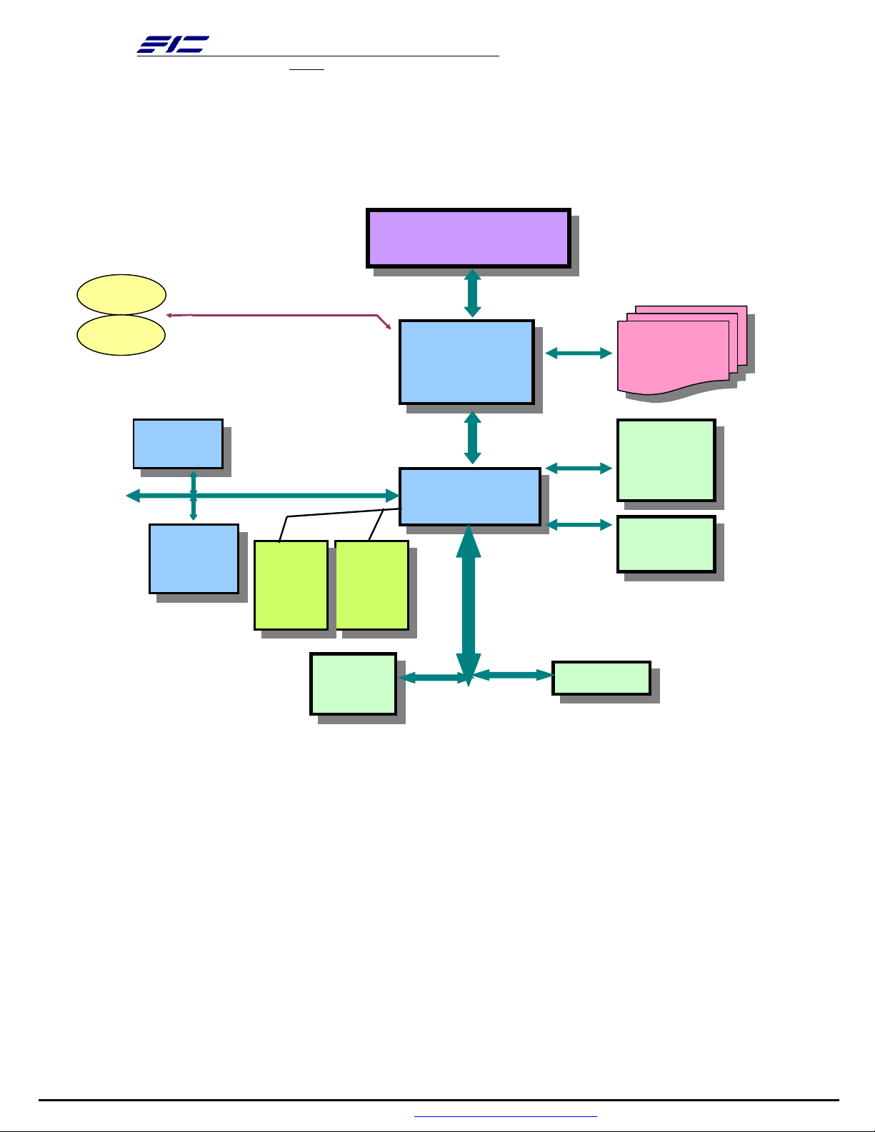
Main components block diagram:
Intel uFCPGA
NorthBridge
Montara
DDR
SDRAM
Cardbus
/1394
Mini PCI
South Bridge
Audi
o
AC’9
7
HDD
CDRO
USB
KBC
8
- -
PDF created with FinePrint pdfFactory trial version http://www.fineprint.com
Page 9

FIRST INTERNATIONAL COMPUTER,
INC.
9
- -
PDF created with FinePrint pdfFactory trial version http://www.fineprint.com
Page 10
FIRST INTERNATIONAL COMPUTER,
Synthesiz
INC.
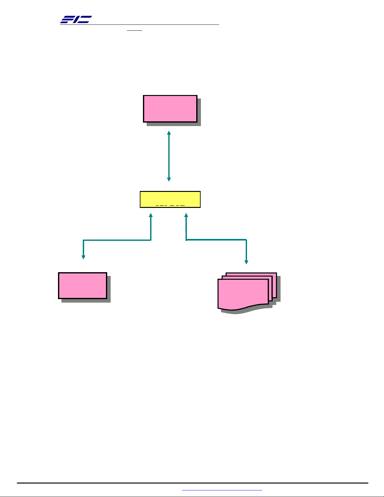
ICH4 SMBUS block diagram:
ICH4
Clock
SMB
SDRAM
SOCKET
PMU08 SMBUS block diagram:
10
- -
PDF created with FinePrint pdfFactory trial version http://www.fineprint.com
Page 11
FIRST INTERNATIONAL COMPUTER,
SMBUS
INC.
PMU08
PIC
Battery
MAX1617
OZ168
11
- -
PDF created with FinePrint pdfFactory trial version http://www.fineprint.com
Page 12

FIRST INTERNATIONAL COMPUTER,
INC.
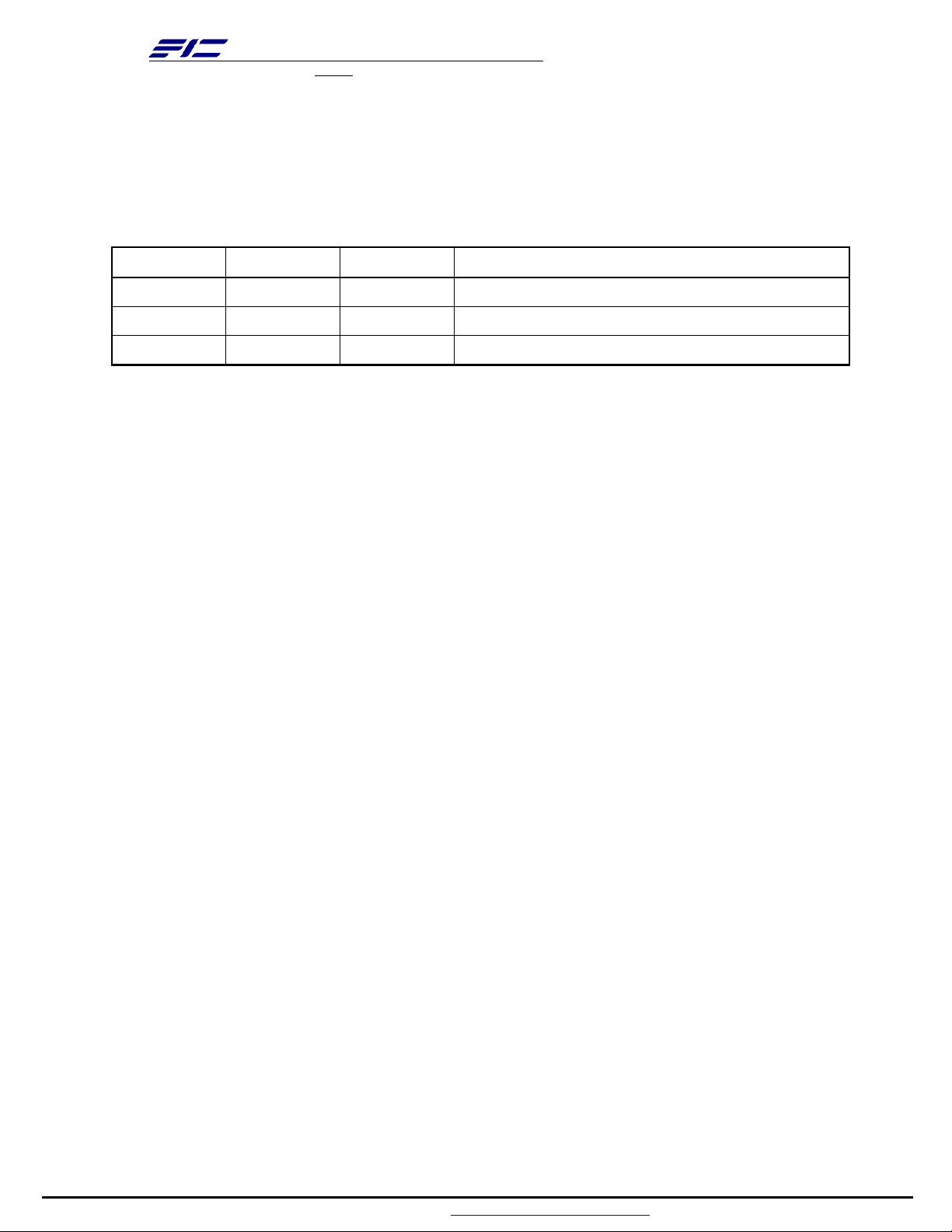
2.1 H/W Key Part List
Controller
Vender Description
Chip
Processor Intel Mobile Banias
North Bridge Intel MontaraGM
South Bridge Intel ICH4
Video Controller
PCMCIA
Intel Embedded in MontaraGM
RICOH R5C551
Controller
Audio Controller
Intel South Bridge Integrated
Audio Codec Intel ICH4
Keyboard
Misubishi M3885x
Controller
Power
NEC PMU08
Management
ROM BIOS SST 49LF004A
Clock Generator IMI CY28346
Temperature
NS MAX6690
Sensor
IEEE 1394 RICOH R5C551
LAN Intel ICH4
Modem Intel MDC AC’97
2.2 Marketing Related Spec.
Controller
Description
Chip
CPU Intel uFCPGA Banias
Level 2 Cache 1024KB L2 Cache
12
- -
PDF created with FinePrint pdfFactory trial version http://www.fineprint.com
Page 13

FIRST INTERNATIONAL COMPUTER,
INC.
System Memory § Two SO-DIMM sockets that can support up to 512MB
(Max)
§ PC-200/266 DDR SDRAM Specification
§ Base socket: 128/256/512MB, Expansion socket:
128/256/512MB
Video RAM UMA (8 ~32MB)
BIOS ROM 512KB flash ROM with boot block
HDD 2.5” 9.5mmH Pack
CD-ROM 24x CD-ROM
CD-R/W 8x CD-R, CD-RW
Combo 8x DVD, 8x CD-R, CD-RW write, 20x CD-ROM(read
only)
DVD-ROM 8x DVD
LCD Panel § 14.1” XGA LCD
Audio Software Audio , compliant with AC97
PCMCIA/1394 PCMCIA-Hot plug w/o external buffer/IEEE1394-Data
rate 100/200/400 Mbits per second.
Keyboard Support 2 extra Win 95 hot keys (87/88 KEYS)
Pointing Device Built-in glide pad with 2 buttons
Modem AC97 Modem
LED Indicators
§ IDE accessing LED (Blue)
§ Caps lock LED (Blue)
§ Scroll lock LED (Blue)
§ Num lock LED (Blue)
§ Battery in charging LED (Blue)
§ Power Status LED (Blue when power on, Blue Blinking
when system enter suspend mode, Turn off when Battery
Low)
13
- -
PDF created with FinePrint pdfFactory trial version http://www.fineprint.com
Page 14

FIRST INTERNATIONAL COMPUTER,
INC.
Ports
Switches and
Buttons
Options
CRT D-sub 15pin*1
USB 3pin*2 port (Ver1.1/2.0)
IEEE1394 One port
Cardbus One port
Mic In Min Jack *1
Modem RJ11*1
LAN RJ45*1
§ Power switch (Power/Suspend button)
§ Lid switch (Cover switch)
§ Expanded RAM module (SO-DIMM type)
§ Battery pack
§ AC Adapter
14
- -
PDF created with FinePrint pdfFactory trial version http://www.fineprint.com
Page 15

FIRST INTERNATIONAL COMPUTER,
INC.
3. Summary Of BIOS Spec.
Controller
Description
Chip
BIOS Feature § Microsoft PC99 logo and WinXP logo approval.
§ Support Boot Block / Crisis Rescue.
§ APM 1.2 Compliance
§ Support ACPI 1.0B (or above) Spec.
§ Support PCI 2.1 (or above) Spec.
§ Support SMBIOS 2.3 (or above) Spec
§ Support Windows XP.
§ Support flash function including both DOS and Windows
interface for new BIOS update.
§ Support US keyboard .
§ Support boot from LAN , USB FDD/FLASH , HDD and
CDROM Drive.
§ Support Phoenix First BIOS.
CPU Auto detecting the CPU type and speed for Intel Banias
based system.
Support Intel Geyserville III Technology .
DRAM Auto sizing and detection. Support PC-200/266 DDR
SDRAM.
Cache § Level 2 SRAM auto sizing and detection.
§ Always enable CPU L1 and L2 cache.
Shadow Always enable VGA and System BIOS shadow.
Display § System auto detects LCD or CRT presence on boot .
§Up to 32 MB of Dynamic Video Memory Allocation.
15
- -
PDF created with FinePrint pdfFactory trial version http://www.fineprint.com
Page 16

FIRST INTERNATIONAL COMPUTER,
INC.
Hard Disk § Enhanced IDE spec.
§ Support auto IDE detection.
§ Support LBA mode for larger capacity HDD.
§ Support Ultra DMA 33/66/100.
§ Support Fast PIO mode 1-4 transfer.
§ Support 32 bit PIO transfer.
§ Support Multi-Sector transfer.
§ Support SMART monitoring.
Multi Boot Allow the user to select boot from USB FDD/FLASH, HDD
LAN and CD-ROM.
Plug and Play Support PnP Run Time Service and conflict-free allocation
of resource during POST
Smart Battery Support BIOS interface to pass battery information to the
application via SMBus.
Keyboard
Controller
Support Fn hot keys, two Win95 hot keys, built-in Glide
Pad.
PCMCIA Compliant with PCMCIA 2.1 specification.
Power Management
Support (ACPI
Mode)
The power management is compliant with ACPI 1.0B
specification and supports the following power state:
§ S0 (Full-On) Mode
§ S3 (STR) Mode
§ S4 (STD) Mode
§ S5 (Soft-Off) Mode
16
- -
PDF created with FinePrint pdfFactory trial version http://www.fineprint.com
Page 17

FIRST INTERNATIONAL COMPUTER,
INC.
4. System
4.1 System Memory
The system memory consists of DDR SDRAM memory on 64-bit bus and the size options are
64/128/256MB. The BIOS will automatically detect the amount of memory in the system and
configure CMOS accordingly during the POST (Power On Self Test) process. This must be done in a
way that requires no user interaction.
DRAM Combination Configuration
Base SO-DIMM
DRAM slot
Expansion SO-DIMM
DRAM slot
(Bank 0&1) (Bank 2&3)
NIL 128MB 128MB
NIL 256MB 256MB
NIL 512MB 512MB
128MB NIL 128MB
128MB 128MB 256MB
128MB 256MB 384MB
128MB 512MB 640MB
256MB NIL 256MB
256MB 128MB 384MB
256MB 256MB 512MB
256MB 512MB 768MB
512MB NIL 512MB
512MB 128MB 640MB
Total Size
512MB 256MB 768MB
512MB 512MB 1024MB
4.2 Video
17
- -
PDF created with FinePrint pdfFactory trial version http://www.fineprint.com
Page 18

FIRST INTERNATIONAL COMPUTER,
INC.
4.2.1 Supported Video Mode
The following is the display modes supported by the INTEL Mobility Video
control in LCD only, CRT only, and simultaneous mode. The VGA BIOS will
allow mode sets of resolutions greater than the panel size but only show as
much mode display as will fit on the panel.
Supported standard VGA modes:
The VGA BIOS supports the IBM VGA Standard 7-bit VGA modes numbers.
Mode Pixel Resolution Colors Memory
00h/01h 40*25 16 Text
02h/03h 80*25 16 Text
04h/05h 320*200 4 2-bit Planar
06h 640*200 2 1-bit Planar
07h 80*25 Mono Text
0Dh 320*200 16 4-bit Planar
0Eh 640*200 16 4-bit Planar
0Fh 640*350 Mono 1-bit Planar
10h 640*350 16 4-bit Planar
11h 640*480 2 2-bit Planar
12h 640*480 16 4-bit Planar
13h 320*200 256 8-bit Planar
Note: All Standard VGA Modes are limited to the standard VGA refresh rates.
Supported extended video modes:
CRT device will support all listed VESA mode; and other devices such as PANEL
& TV may be limited to the mode support due to their characteristics.
VESA
Mode
Pixel
Resolution
Memory Model Refresh Rates In
(Hz)
Minimum
Memory
100h 640 x 400 8-bit Packed 70 2MB
101h 640 x 480 8-bit Packed 60, 72, 75, 85 2MB
102h 800 x 600 4-bit Planar 60, 72, 75, 85, 100
18
- -
PDF created with FinePrint pdfFactory trial version http://www.fineprint.com
2MB
Page 19

FIRST INTERNATIONAL COMPUTER,
INC.
103h 800 x 600 8-bit Packed 60, 72, 75, 85, 100
104h 1024 x 768 4-bit Planar 43(I), 60, 70, 75,
2MB
2MB
85, 100
105h 1024 x 768 8-bit Packed 43(I), 60, 70, 75,
2MB
85, 100
106h 1280 x 1024 4-bit Planar 43(I), 60, 75, 85 2MB
107h 1280 x 1024 8-bit Packed 43(I), 60, 75, 85 2MB
10Eh 320 x 200 16-bit Packed 70 2MB
10Fh 320 x 200 32-bit Unpacked
70 2MB
111h 640 x 480 16-bit Packed 60, 72, 75, 85 2MB
112h 640 x 480 32-bit Unpacked
114h 800 x 600 16-bit Packed 60, 72, 75, 85, 100
115h 800 x 600 32-bit Unpacked 60, 72, 75, 85, 100
117h 1024 x 768 16-bit Packed 43(I), 60, 70, 75,
60, 72, 75, 85 2MB
2MB
2MB
2MB
85, 100
118h 1028 x 768 32-bit Unpacked 43(I), 60, 70, 75,
4MB
85, 100
11Ah 1280 x 1024 16-bit Packed 43(I), 60, 75, 85 4MB
11Bh 1280 x 1024 32-bit Unpacked
43(I), 60, 75, 85 8MB
11Dh 640 x 400 16-bit Packed 70 2MB
11Eh 640 x 400 32-bit Packed 70 2MB
120h 1600 x 1200 8-bit Packed 48(I), 60, 75, 85 2MB
122h 1600 x 1200 16-bit Packed 48(I), 60, 75, 85 4MB
124h 1600 x 1200 32-bit Unpacked
48(I), 60, 75, 85 8MB
12Ah 640 x 480 24-bit Packed 60, 72, 75, 85 2MB
12Bh 800 x 600 24-bit Packed 60, 72, 75, 85, 100
12Ch 1024 x 768 24-bit Packed 43(I), 60, 70, 75,
2MB
4MB
85, 100
12Dh 1280 x 1024 24-bit Packed 43(I), 60, 75, 85 4MB
12Eh 320 x 200 8-bit Packed 70 2MB
131h 320 x 200 8-bit Packed 72 2MB
19
- -
PDF created with FinePrint pdfFactory trial version http://www.fineprint.com
Page 20

FIRST INTERNATIONAL COMPUTER,
INC.
133h 320 x 200 16-bit Packed 72 2MB
134h 320 x 200 32-bit Packed 72 2MB
13Bh* 1400 x 1050 8-bit Packed 60, 75 2MB
13Ch* 1400 x 1050 16-bit Packed 60, 75 4MB
13Eh* 1400 x 1050 32-bitUnpacked
60, 75 8MB
141h 400 x 300 8-bit Packed 72 2MB
143h 400 x 300 16-bit Packed 72 2MB
144h 400 x 300 32-bitUnpacked
72 2MB
151h 512 x 384 8-bit Packed 70 2MB
153h 512 x 384 16-bit Packed 70 2MB
154h 512 x 384 32-bitUnpacked
70 2MB
171h 720 x 480 8-bit Packed 75 2MB
173h 720 x 480 16-bit Packed 75 2MB
174h 720 x 480 24-bit Packed 75 2MB
175h 720 x 480 32-bitUnpacked
75 2MB
176h 720 x 576 8-bit Packed 75 2MB
178h 720 x 576 16-bit Packed 75 2MB
179h 720 x 576 24-bit Packed 75 2MB
17Ah 720 x 576 32-bitUnpacked
75 2MB
Note: “*” The modes may not be available. Their availability should be determined
by VESA function calls.
4.2.2 Panel Type Initialization
The VGA BIOS will issue INT 15h function call during POST. This function
call allows the system BIOS to specify the panel type to the VGA BIOS. The
system BIOS should get the panel type from GPIO pins before the VGA chip
initialized, and pass this information to VGA BIOS through INT 15 Function
5F40h.
20
- -
PDF created with FinePrint pdfFactory trial version http://www.fineprint.com
Page 21

FIRST INTERNATIONAL COMPUTER,
INC.
LCD Panel ID pin Definition:
ICH4 GPI Pins
GPIO 3 GPIO 2 GPIO 1 GPIO 0
Panel Type
0 0 0 0
0 0 0 1 ID0
0 0 1 0 ID1
0 0 1 1
0 1 0 0 ID2
0 1 0 1
0 1 1 0
0 1 1 1
1 0 0 0 ID3
1 0 0 1
1 0 1 0
1 0 1 1
1 1 0 0
1 1 0 1
1 1 1 0
1 1 1 1
4.3 Enhanced IDE
The system BIOS must be ready to support 4 IDE devises on two controllers. The BIOS support
Ultra DMA33/66/100 and also supports automatic configuration of drives using both the LBA and
CHS large drive remapping method. In addition to supporting standard drives through an
auto-configuration process that does NOT require user involvement or confirmation. The system
should automatically do this at POST time in a way that is transparent to the user. If a drive is
connected to the bus, the drive should be automatically recognized, configured and available for use
under MS-DOS 6.2x.
4.4 Audio
The audio subsystem will support the requirements identified by the AC 97
specification. Both software and hardware will control the volume level for the
internal audio subsystem. In addition to volume control, the user will be able to
21
- -
PDF created with FinePrint pdfFactory trial version http://www.fineprint.com
Page 22

FIRST INTERNATIONAL COMPUTER,
INC.
mute the sound to completely cut off the volume using both software and
hardware.
4.5 PCMCIA/IEEE 1394
R5C551 is the single chip solution offering PCI bus-PC Card bridge and PCI bus-IEEE 1394 OHCI
bridge with integrated PHY.The R5C551 is compliant with the latest specification in both PC card and
IEEE 1394.
4.6 LED Indicator
Indicator Function Description
IDE accessing
This LED will turn on while accessing the IDE Device.
LEDŒ
Battery Charging
LED
Turn on (Blue) – Battery is under charging mode
Turn off – Battery full charged or no battery
CapsLock LEDΠThis LED will turn on when the function of CapsLock is
active.
ScrollLock LEDΠThis LED will turn on when the function of ScrollLock is
active.
NumLock LEDΠThis LED will turn on when the function of NumLock is
active.
Power Status LED
Blue – System is powered on.
Blue Blinking- System is entered suspend mode.
Trun off – Battery Low.
Mail LEDΠThis LED will turn on while Mail was arrived.
NoteŒ: These LEDs will be turned off during Suspend mode.
4.7 Hot Keys Definition
All Hot keys must be active at all times under all operation systems.
22
- -
PDF created with FinePrint pdfFactory trial version http://www.fineprint.com
Page 23

FIRST INTERNATIONAL COMPUTER,
INC.
4.7.1 Hot Keys by Internal Keyboard
Function Function Handler
Fn + F3 Toggle Display
BIOS Handler
(LCD/CRT/TV/LCD&CRT)
Fn + F2 RF ON/OFF BIOS Handler
Fn + F6 System Speaker On/Off BIOS Handler
Fn + F8 Brightness Increase Controlled by PMU08
Fn + F9 Brightness Decrease Controlled by PMU08
ScrLock Scroll Lock
Internet
Internet Function Key Controlled by Driver
Button
Mail Button Mail Function Key Controlled by Driver
Note: The scale parameters of the brightness will be saved in CMOS before
Suspend to Disk and SoftOff.
4.8 Plug & Play
The BIOS supports the Plug and Play Specification 1.0A. (Include ESCD)
This section describes the device management. The system board devices and its resources are as
follows.
Device Connect
Resources
Type
I/O IRQ DMA
DMA Controller
Interrupt
Controller
Static 00~0F, 81~8F
Static 20~21,
A0~A1
- DMA
IRQ2 - -
System Timer Static 40~43 IRQ0 - -
RTC Static 70~71 IRQ8 - -
ISA Bus Static - - - -
23
- -
PDF created with FinePrint pdfFactory trial version http://www.fineprint.com
Memory
-
5
Page 24

FIRST INTERNATIONAL COMPUTER,
INC.
System Speaker
Static 61 - - -
System Board Static - - - E0000~FFFFF
PnP Mother
Static 80 - - -
Board
Keyboard
Static 60, 64 IRQ1 - -
Controller
PMU08
Static 68, 6C - - -
Controller
Math
Static F0~FF IRQ13
- -
Coprocessor
Glide Pad Static - IRQ12
Video Controller
Static 3B0~3BB,
3C0~3DF
Dual IDE
Controller
Static 170~177,
1F0~1F7,
IRQ5 - A0000~BFFFF,
IRQ14,
15
- -
C0000~CFFFF
- -
3F6
CardBus
Dynamic
3E0~3E1 IRQ10
- -
Controller
Audio chip Dynamic
IEEE1394 Dynamic
Modem Dynamic
LAN Dynamic 1080~10FF IRQ10
USB Host
Dynamic EF80~EF9F IRQ5 - -
Controller
IDSEL Pin
PCI Device
220~22F,
IRQ5 DMA
300~301,
388~38B
IRQ10
3E8~3EF IRQ10
4.9 PCI Device
IDSEL Pin Allocation:
24
- -
-
3
- -
- -
PDF created with FinePrint pdfFactory trial version http://www.fineprint.com
Page 25

FIRST INTERNATIONAL COMPUTER,
INC.
Device
Number
Function
Number
Device Name
AD23 Device 07 Function 0 RICOH Card Bus
Function 1 RICOH IEEE1394
AD17 Device 01 Function 0 MINI PCI
INT Pin Allocation:
INT Pin PCI Device
INTA CardBus/MiniPCI/LAN
INTB Cardbus/MiniPCI
INTC
INTD
PCI Bus Master Allocation:
Arbiter Signal Agents
Function Use
(Master)
REQ00/GNT0
0
REQ10/GNT1
RICOH Card Bus Controller
0
REQ20/GNT2
0
REQ30/GNT3
0
25
- -
PDF created with FinePrint pdfFactory trial version http://www.fineprint.com
Page 26

FIRST INTERNATIONAL COMPUTER,
INC.
4.10 SMBus Devices
The SMBus is a two-wire interface through which the system can communicate
with power-related chips. The BIOS should initialize the SMBus devices during
POST.
4.10.1 Ich4 SMBus Connection Devices
SMBus Device Host/Slave Addre
ss
SO-DIMM Slave A0h/A
2h
CY28346
Slave D2h Program the desired clock
CLK Generator
4.10.2 PMU 08 SMBus Connection Devices
SMBus Device Host/Slave Addre
ss
A7 ~
A1
BIOS Need to Initialization
Memory Auto Sizing (SPD).
frequency (Pin23 output
24MHz, Pin22 output 48MHz)
BIOS Need to Initialization
PMU08 Master 10h Enable PS01 decode interface
MAX6690 (Thermal
Slave 9Ch Program the desired
sensor)
Battery (1st Battery) Slave A8h No Need
4.11 Resource Allocation
4.11.1 I/O Map
26
- -
PDF created with FinePrint pdfFactory trial version http://www.fineprint.com
temperature range
Page 27

FIRST INTERNATIONAL COMPUTER,
INC.
Hex
Device
Address
000 - 01F 8237-1
020 - 021 8259-1
022
040 - 05F 8254
060 - 064 Keyboard Controller
068 – 06C PMU08 Controller
070 - 07F RTC & NMI Mask
080 - 08F DMA Page Registers
092 System Control Port
0A0 - 0A1 8259-2
0B2 Advanced Power Management Control Port
0B3 Advanced Power Management Status Port
0C0 – 0DF 8237-2
0F0 – 0FF Math Coprocessor
170 - 177 IDE Secondary Command Block
1F0 - 1F7 IDE Primary Command Block
220 - 22F Sound Blaster
279 ISA PnP Address
330 - 333 MIDI
376 IDE Secondary Control Block
388 - 38B FM Synthesizer
3B0 - 3DF Video Controller
3E0 - 3E1 PCMCIA Controller
3F0 - 3F5, 3F7
Floppy Disk Controller
3F6 IDE Primary Control Block
A79 ISA PnP Address
CF8 – CFF PCI BUS configuration Register
27
- -
PDF created with FinePrint pdfFactory trial version http://www.fineprint.com
Page 28

FIRST INTERNATIONAL COMPUTER,
INC.
4.11.2 ISA DMA Map
DMA Channel
Device
DMA 0 Unused
DMA 1 Unused
DMA 2 Floppy Disk
DMA 3 Audio
DMA 4 Unused
DMA 5 Unused
DMA 6 Unused
DMA 7 Unused
4.11.3 Memory Map
Address Range Length Description
00000 - 9FFFFh 640 KB System Memory
A0000 – BFFFFh
C0000 – C9FFFh
CA000 – DBFFFh
128 KB Video Memory
40 KB Video ROM
72 KB Unused
DC000 - DFFFFh
16 KB DMI information
E0000 – FFFFFh 128 KB System ROM BIOS
4.11.4 IRQ Map
IRQ# Description
IRQ 0 System Timer
IRQ 1 Keyboard
IRQ 2
IRQ 3
IRQ 4
IRQ 5 Audio/VGA/USB
IRQ 6 Floppy Disk Drive
IRQ 7
28
- -
PDF created with FinePrint pdfFactory trial version http://www.fineprint.com
Page 29

FIRST INTERNATIONAL COMPUTER,
INC.
IRQ 8 RTC Alarm
IRQ 9 ACPI
IRQ10 LAN / Modem or Combo, (Card Bus), IEEE 1394
IRQ11 Reserved for PCMCIA card
IRQ12 Glide Pad
IRQ13 FPU (FERR)
IRQ14 Hard Disk Drive
IRQ15 CD-ROM or DVD-ROM
4.12 GPIO Pin Assignment
The GPI and GPO pins connected to system devices. The BIOS can get device’s status and control the
device via the GPI and GPO pins.
4.12.1 ICH4 GPIOs pin assignment
GPIO
Number
Signal
Name
Defau
lt
I/O Notes
GPIO0 PanelID0 I Panel ID setting
GPIO1 PanelID1 I Panel ID setting
GPIO2 PanelID2 I Panel ID setting
GPIO3 PanelID3 I Panel ID setting
GPIO8
GPIO11 LPC_QPM
Q_SMI0 I 0:External K/B SMI0
1:Normal operation
1 O 0:LPC_QPME0 Event
E0
Enable
1:Normal operation --
GPIO12 EC_SCI0 I 0:PMU SCI Detect
1:PMU SCI not Detect
GPIO13
PM_RI0 I 0:PMU GPIO detect
1:PMU GPIO not Detect
29
- -
PDF created with FinePrint pdfFactory trial version http://www.fineprint.com
Page 30

FIRST INTERNATIONAL COMPUTER,
INC.
GPIO25 CB_HWSU
SP0
GPIO32 SPDMUX0
GPIO33
SPDMUX1
GPIO
number
GPIO
B6
GPIO
Signal
Name
PM_SLP_
S10
N.C. -- -- No used
B5
1 O R5C551 Hardware suspend
control pin
1 O SMBus select 1
1 0 SMBus select 0
4.14.2 PMU08 GPIO pin assignment
Defau
I/O Notes Rem
lt
1 I Suspend Plane A control
for ICH4
0: POS, STR and STD
suspend state.
1: not suspend state.
ark
GPIO
B4
GPIO
B1
GPIO
B0
GPIO
A7
GPIO
A6
GPIO
A0
N.C. -- -- No used
N.C. 1 O No used
N.C. -- -- No use
N.C -- -- No use
PCMRI0 1 I PC Card Ring event
0: Ring
1: No Ring
LID0 1 I LCD Open/Close Status
0: LCD Close
1: LCD Open
30
- -
PDF created with FinePrint pdfFactory trial version http://www.fineprint.com
Page 31

FIRST INTERNATIONAL COMPUTER,
INC.
GPIO
C1
GPIO
B7
GPIO
B2
GPIO
B0
GPIO
A5
GPIO
A4
GPIO
A1
GPIO
C2
NC -- -- No Use
PM_RI0 1 O Wake Up event request
0: Wake SMI(SCI)
1: There is no demand.
N.C. -- - No Use
N.C. -- -- No Use
PRSTMS
K0
1 O PCI Reset Mask
0: Reset Mask
1: Reset Enable
PCMUTE
1 O Mute PC Speaker
0
N.C. -- -- No use
CHGLED
Charge Battery indicator :
1 : charging Battery
0 : Stop charging Battery
GPIO
N.C. -- -- No Use
C3
GPIO
N.C. -- -- No Use
C0
5. ACPI
5.1 General Requirements
The BIOS must meet the following general Power Management requirements:
Refers to the portion of the firmware that is compatible with the ACPI 1.0b
specifications.
Support for Power ON(S0 state), Suspend-to-RAM (S3 state) , Suspend-to-Disk
31
- -
PDF created with FinePrint pdfFactory trial version http://www.fineprint.com
Page 32

FIRST INTERNATIONAL COMPUTER,
INC.
mode (S4 state) and Soft OFF(S5 state).
5.2 Global System State Definitions
Global system states (Gx states) apply to the entire system and are visible to the
user.
Following is a list of the system states:
G0/S0 - Working:
A computer state where the system dispatches user mode (application) threads
and they execute. In this state, devices (peripherals) are dynamically having their
power state changed. The user will be able to select (through some user interface)
various performance/power characteristics of the system to have the software
optimize for performance or battery life. The system responds to external events in
real time. It is not safe to disassemble the machine in this state.
G1 - Sleeping:
A computer state where the computer consumes a small amount of power, user
mode threads are not being executed, and the system “appears” to be off (from an
end user’s perspective, the display is off, etc.). Latency for returning to the
Working state varies on the wakeup environment selected prior to entry of this
state (for example, should the system answer phone calls, etc.). Work can be
resumed without rebooting the OS because large elements of system context are
saved by the hardware and the rest by system software. It is not safe to disassemble
the machine in this state.
G2/S5 - Soft Off:
A computer state where the computer consumes a minimal amount of power. No
user mode or system mode code is run. This state requires a large latency in order
to return to the Working state. The system’s context will not be preserved by the
hardware. The system must be restarted to return to the Working state. It is not
safe to disassemble the machine.
G3 – Mechanical Off:
A computer state that is entered and left by a mechanical means. It is implied by
the entry of this off state through a mechanical means that the no electrical
current is running through the circuitry and it can be worked on without
damaging the hardware or endangering the service personnel. The OS must be
32
- -
PDF created with FinePrint pdfFactory trial version http://www.fineprint.com
Page 33

FIRST INTERNATIONAL COMPUTER,
INC.
restarted to return to the Working state. No hardware context is retained. Except
for the real time clock, power consumption is zero.
5.3 Sleeping State Definitions
Sleeping states (Sx states) are types of sleeping states within the global sleeping
state, G1. The Sx states are briefly defined below. For a detailed definition of the
system behavior within each Sx state, refer to ACPI specification section 7.5.2. For
a detailed definition of the transitions between each of the Sx states, refer to ACPI
specification section 9.1.
S1 Sleeping State:
The S1 sleeping state is a low wake-up latency sleeping state. In this state, no
system context is lost (CPU or chip set) and hardware maintains all system
context.
S3 Sleeping State:
The S3 sleeping state is a low wake-up latency sleeping state where all system
context is lost except system memory. CPU, cache, and chip set context are lost in
this state. Hardware maintains memory context and restores some CPU and L2
configuration context. Control starts from the processor’s reset vector after the
wake-up event.
S4 Sleeping State:
The S4 sleeping state is the lowest power, longest wake-up latency sleeping state
supported by ACPI. In order to reduce power to a minimum, it is assumed that the
hardware platform has powered off all devices. Platform context is saved in disk.
S5 Soft Off State:
The S5 state is similar to the S4 state except the OS does not save any context nor
enable any devices to wake the system. The system is in the “SOFT” off state and
requires a complete boot when awakened. Software uses a different state value to
distinguish between the S5 state and the S4 state to allow for initial boot operations
within the BIOS to distinguish whether or not the boot is going to wake from a
saved memory image.
5.4 System Power Plane
The system components are grouped as the following parties to let the system to control the On/Off
33
- -
PDF created with FinePrint pdfFactory trial version http://www.fineprint.com
Page 34

FIRST INTERNATIONAL COMPUTER,
INC.
of power under different power management modes.
The power plane is divided as following:
Power
Group
Power
Control Pin
Controlled Devices
+B Nil IMM, (9V~20V)
+3VA Nil RTC I/F, PMU08
+12V PWRON PCMCIA Card, AC97 Codec
+5V PWRON PCMCIA Slot 5V
+3V PWRON VGA, PCMCIA, PCMCIA Slot 3V, DRAM,
Twister(DRAM I/F), M3885x, MAX3243
+5VS SUSB# FLASH ROM, HDD, CD-ROM, USB, Internal K/B,
Glide Pad, Audio AMP, Fan
+3VS SUSB# ISA I/F Power, Clock Generator & Buffer (W137)
+RTCVC
Nil RTC
CS
34
- -
PDF created with FinePrint pdfFactory trial version http://www.fineprint.com
Page 35

FIRST INTERNATIONAL COMPUTER,
INC.
5.5 Power Management Mode Transition Flow Chart
S1
Sleeping
SLP_TYPx=S1
and
SLP_EN
SLP_TYPx=S2
and
SLP_EN
SLP_TYPx=S3
and
SLP_EN
SLP_TYPx=S4
and
SLP_EN
S2
Sleeping
G1
S3
Sleeping
S4
G2 (S5) -
Soft Off
ACPI
Boot
(SCI_EN=1)
SLP_TYPx=S5
and
SLP_EN
or
PWRBTN_OR
Wake
Event
G0 (S0) -
Working
S4BIOS_REQ
to
SMI_CMD
Sleeping
OEM S4 BIOS
Handler
SLP_TYPx=S4
and
SLP_EN
5.6 Power States transition event
The following table summarize the entry events and wake-up events of each
power state
Power State
Entry Event Wake up Event
S3 OSPM control
Lid Close
Power Button
Sleep Button
Battery Low
35
- -
PDF created with FinePrint pdfFactory trial version http://www.fineprint.com
Power Button
Ring Wake up
RTC Alarm
LAN Wake Up
Lid open
Page 36

FIRST INTERNATIONAL COMPUTER,
INC.
S4 OSPM control,
Power button
Power Button
RTC Alarm
Sleep button
Lid Close
Battery Low
S5 Power Button
Battery Low
Power Button
OSPM control
x OSPM: OS-directed Power Management
5.7 Device Power Control Methodology
5.7.1 Power state of local devices table
This section illustrates the power control status of each key device/component of the system under
each power management mode.
PowerState
Doze Stand By STR STD/SOff
Component
CPU Stop
L2 CACHE
Grant
ON Power
Stop
Clock
Power Off Power Off
Power Off Power Off
Down
MontaraGM
ON Stop
Clock
Power Off (except
Vcc)
ICH4 ON ON Power Off (except
SUSVcc, RTCVcc )
DRAM ON Self
Self Refresh Power Off
Refresh
Clock
Synthesizer
CDROM ON Power
ON Low
Power
Power Off Power Off
Power Off Power Off
Down
36
- -
Power Off
Power Off (except
SUSVcc, RTCVcc)
PDF created with FinePrint pdfFactory trial version http://www.fineprint.com
Page 37

FIRST INTERNATIONAL COMPUTER,
INC.
HDD ON Power
Power Off Power Off
Down
FDD ON Power
Power Off Power Off
Down
KBC ON ON Power Down Power Off
PMU08 ON ON Power Down Power Down
VGA/VRA
M
PCMCIA ON Power
ON Power
Down
Power Down Power Off
Power Down Power Off
Down
AUDIO ON Power
Power Off Power Off
Down
Audio AMP
ON Power
Power Off Power Off
Down
LCD
ON Power Off
Power Off Power Off
Backlight
LAN ON Power
Power Down Power Down
Down
Internal
Modem
ON Power
Down
Power Down Power Down
5.7.2 Device Power Control Methodology During S3(Suspend to RAM) Mode
This section illustrates the control methodology of each device/component and its details under
Suspend to RAM mode.
Device Power Down
Description
Controlled by
CPU Hardware Controlled by SUSB# pin
L2 CACHE Hardware Power off
ICH4 Hardware Controlled by SUSB# pin
DRAM Software Self Refresh
Clock Synthesizer Hardware Controlled by SUSB# pin
37
- -
PDF created with FinePrint pdfFactory trial version http://www.fineprint.com
Page 38

FIRST INTERNATIONAL COMPUTER,
INC.
CDROM Hardware Power off
HDD Hardware Power off
FDD Hardware Power off
KBC Software Controlled by M3885xM8 power
down command
PMU08 Sofeware Controlled by PMU08 power
down command
VGA/VRAM Software Controlled by MontaraGM
PCMCIA Software Controlled by SUSB# pin
AUDIO Hardware Controlled by ICH4
Audio AMP Hardware Controlled by BIOS
LCD Backlight Hardware Power off
LAN Hardware Controlled by Driver enter Dx
status
Internal Modem Hardware Controlled by Driver enter Dx
ststus
5.8 Power Button
The function of Lid Switch is depends on the ACPI aware OS.
5.9 Lid Switch (Cover Switch)
The function of Lid Switch is depends on the ACPI aware OS.
38
- -
PDF created with FinePrint pdfFactory trial version http://www.fineprint.com
Page 39

FIRST INTERNATIONAL COMPUTER,
EC
ACI
RI1 PCM
LID
KBS
ICH4
INC.
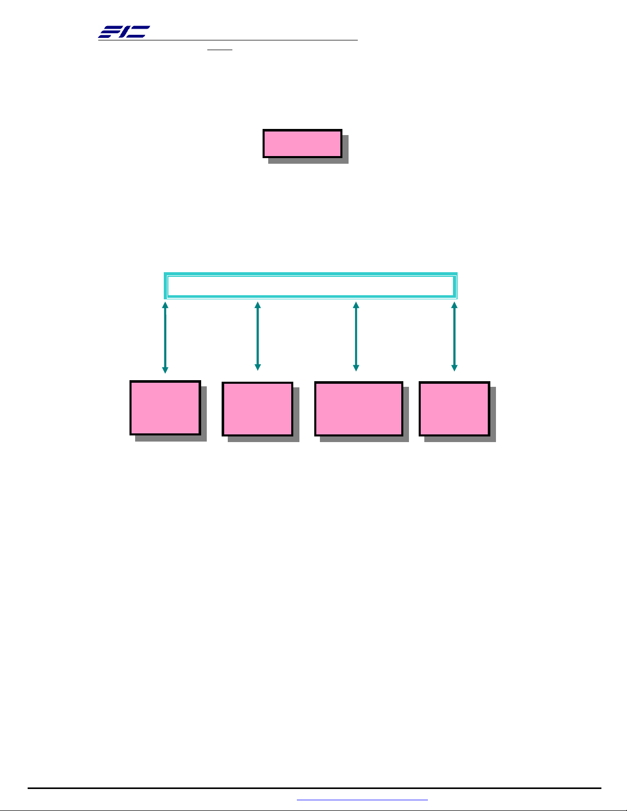
5.10 Expanding Event Through the Embedded Controller
The following figure shows the relationships between the devices that are wired to the embedded
controller, the embedded controller queries, and the ACPI specified General
THR
GPI8
GPI1
GPI13
39
- -
PDF created with FinePrint pdfFactory trial version http://www.fineprint.com
Page 40

FIRST INTERNATIONAL COMPUTER,
INC.
5.10.1 SCI Source and GPE Event from PMU08
PMU08 Input Event GPE Event Handler
ADPIN# AC Plug In/Out GPI12 AML Handler
BAT0# Battery Plug In/Out GPI12 AML Handler
GPIOA0 LID Event GPI13 AML Handler
GPIOA3 Keyboard SMI GPI8 AML Handler
GPIOA6 PCMCIA Ring In GPI13 AML Handler
GPIOA7 COM Port Ring In GPI13 AML Handler
THRM Thermal Event GPI12 AML Handler
5.10.2 Control Method Battery Subsystem
EC should support all the battery information to ACPI-OS
Designed Battery capacity
Designed Voltage
Designed battery waring capacity
Designed battery low capacity
Latest Full charged capacity
Present Remaining capacity
Present drain rate
Present voltage
Present Battery Status
5.11 Thermal Control
There are three primary cooling policies that the OS use to control the thermal state of the hardware.
Cooling Policy
Action
Temperature Setting
Action cooling Fan On Always On
Action cooling Fan High On
Fan High Off
40
- -
PDF created with FinePrint pdfFactory trial version http://www.fineprint.com
Over 70 oC
Below 65oC
Page 41

FIRST INTERNATIONAL COMPUTER,
INC.
Passive cooling Throttling CPU On
Throttling CPU Off
Critical trip point System Shutdown
Over 90 oC
Below 85oC
Over 110 oC
41
- -
PDF created with FinePrint pdfFactory trial version http://www.fineprint.com
Page 42

FIRST INTERNATIONAL COMPUTER,
INC.
6. Battery Management
6.1 Battery Sub-system
§ The charger will stop charge the battery when the following condition is detected.
- The temperature of the system is too high
- The remaining capacity is 95% and more.
Note that the battery life is depend on different configuration running. E.g. with CD-ROM
battery life is shorter, document keyin only battery life is longer, PMU disable battery life is short,
PMU enable battery life is longer.
- Battery reading methodology is through PMU08 SMBus.
6.2 Battery Warning
When the battery voltage is approaching to the Low level, the PMU08 will generate
a battery low SMI/SCI. The system will do the following action.
DOS Mode:
1) The Power Indicator will become blinking.
2) The system will issue a Warning beep.
ACPI Mode:
Depends on user setting .
6.3 Battery Low
When the battery voltage is approaching to the Low level, the PMU08 will generate
a battery low SMI/SCI. The system will do the following action.
DOS Mode:
1) The Power Indicator will keep on Blinking.
2) The system will be power off.
ACPI Mode:
Depends on User setting .
6.4 AC Adapter
When plug in the AC adapter, the system will do the following action:
- The charger will charge the Main Battery, if remaining capacity is not full.
42
- -
PDF created with FinePrint pdfFactory trial version http://www.fineprint.com
Page 43

FIRST INTERNATIONAL COMPUTER,
INC.
- The Battery Charging Indicator will turn on if the battery is in changing mode.
43
- -
PDF created with FinePrint pdfFactory trial version http://www.fineprint.com
Page 44

FIRST INTERNATIONAL COMPUTER,
W
W
W
W
W
W
W
INC.
7. PMU08
The Embedded controller PMU08 acts as a supplement for power management control. It supports a lot of
functions via SMBus interface.
7.1 The System EC RAM With PMU08
Embedded Controller Command Set
The EC I/F command set allows the OS to communicate with the PMU08.
For detail information refer to ACPI 1.0B specification.
Comm
EC I/F Command
and
Byte
Encodi
ng
By
te
Regis
ter
R
Description Interrupt
/
Read Embedded
Controller
(RD_EC)
Write Embedded
Controller
(WR_EC)
Burst Enable
Embedded
0x80
#1 EC_S
C
#2 EC_
DAT
A
#3 EC_
DAT
A
0x81
#1 EC_S
C
#2 EC_
DAT
A
#3 EC_
DAT
A
0x82 #1 EC_S
C
Command
byte Header
Address byte
to read
R Read data
to host
Command
byte Header
Address byte
to write
Data to
write
Command
byte Header
Interrupt
on IBF=0
No
Interrupt
Interrupt
on OBF=1
Interrupt
on IBF=0
Interrupt
on IBF=0
Interrupt
on IBF=0
No
Interrupt
44
- -
PDF created with FinePrint pdfFactory trial version http://www.fineprint.com
Page 45

FIRST INTERNATIONAL COMPUTER,
W
W
INC.
#2 EC_
Burst Disable
Embedded
Controller
(BD_EC)
Query Embedded
Controller
(QR_EC)
DAT
A
0x83 #1 EC_S
C
0x84
#1 EC_S
C
#2 EC_
DAT
A
R
Burst
acknowledge
byte
Command
byte Header
Command
byte Header
R Query value
to host
Interrupt
on OBF=1
Interrupt
on IBF=0
No
Interrupt
Interrupt
on OBF=1
45
- -
PDF created with FinePrint pdfFactory trial version http://www.fineprint.com
Page 46

FIRST INTERNATIONAL COMPUTER,
76
0
*3
*3
*3
*3
*3
*3
INC.
7.2 PMU08 EC RAM List
The micro controller PMU08 acts as a supplement for power management control. It supports the
following functions via SMBus Command ( 0x80 , 0xC0 )
Registe
Func
tion
A
dd
re
r
Name
Bit Number
R/
W
Logic
5 432 1
De
fau
lt
Description
ss
1st
Batte
ry
[ _BI
F ]
00
h
02
h
04
h
06
h
08
h
Power
unit
Design
capacit
y
Last
Full
Charge
Capaci
ty
Batter
y
Techno
logy
Design
Voltag
e
R(
DATA[15:0]
/
W
)
R(
/
DATA[15:0]
W
)
R(
DATA[15:0]
/
W
)
R(
/
DATA[15:0]
W
)
R(
DATA[15:0]
/
W
)
*1
*1
*1
*1
*1
0xf
fff
value]
0xffff: Unknown
0x0000: mWh [Fixed
0xf
-
-
fff
0xf
fff
0x0000-0xfffe(mWh)
0xffff: Unknown
0x0000-0xfffe(mWh)
0xffff: Unknown
0x0000 : Primary
0xf
fff
0x0001: Secondary [Fixed
value]
0xffff: Unknown.
0xf
fff
0x0000-0xfffe(mV)
0xffff: Unknown
Design
0
A
h
capacit
y of
Warni
ng
R(
/
DATA[15:0]
W
)
*1
-
46
- -
0xf
fff
PDF created with FinePrint pdfFactory trial version http://www.fineprint.com
0x0000-0xfffe(mWh)
0xffff: Unknown
Page 47

Func
76
0
*3
*3
*3
*3
*3
tion
A
dd
re
ss
0
C
h
0E
h
FIRST INTERNATIONAL COMPUTER,
INC.
Registe
r
Name
Design
capacit
y of
Low
Bit Number
R/
W
R(
/
DATA[15:0]
W
)
5 432 1
*1
Logic
-
Batter
y
capacit
y
Granul
R(
/
DATA[15:0]
W
)
*1
-
arity 1
De
fau
lt
0xf
fff
0xf
fff
Description
0x0000-0xfffe(mWh)
0xffff: Unknown
0x0000-0xfffe(mWh)
0xffff: Unknown
10
h
12
h
14
h
Batter
y
capacit
y
Granul
arity 2
Model
numbe
r
Serial
Numbe
r
R(
DATA[15:0]
/
W
)
R(
/
DATA[15:0]
W
)
R(
DATA[15:0]
/
W
)
*1
*1
*1
0xf
-
-
-
fff
0xf
fff
0xf
fff
0x0000-0xfffe(mWh)
0xffff: Unknown
0x0000 [Not support]
0x0000 [Not support]
47
- -
PDF created with FinePrint pdfFactory trial version http://www.fineprint.com
Page 48

Func
76
0
*3
*3
2: “”
3: “TBCL”
tion
A
dd
re
ss
FIRST INTERNATIONAL COMPUTER,
INC.
Registe
r
Name
Bit Number
R/
W
Logic
5 432 1
De
fau
lt
Description
DAT
16
h
Batter
y type
R(
/
W
)
A[15:
8] *1
All
bits
CEL
L_TY
PE
[7:0]
-
0xf
fff
are 0
CELL_TYPE [3:0] This
code depends on battery
data format. In the future,
this code may be added.
0x00: NiMH
0x01: Li-ion
0x10: Non-rechargeable
battery (Reserved)
Vender [7:0] This code
depends on battery data
format.
And the following name
should be described in the
ASL with the same
character code.
In the future, these codes
will be added.
0: “MoliEnergy”
1: “Panasonic”
18
h
OEM
Inform
ation
R(
/
W
)
DA
TA
[15:
8]
*1
All
Vender[
7:0]
0xf
fff
bits
are
0
(SANYO does not agree the
vender
*1: The register type is word.
*3: This register is not cleared if the system is in S4-S5 state.
R(/W): This is the read only register, but the written data will be able to read back
48
- -
PDF created with FinePrint pdfFactory trial version http://www.fineprint.com
name display)
(Toshiba)
4: “Sony”
Page 49

FIRST INTERNATIONAL COMPUTER,
INC.
till PMU updates the data periodically, or PMU detects the status change.
49
- -
PDF created with FinePrint pdfFactory trial version http://www.fineprint.com
Page 50

FIRST INTERNATIONAL COMPUTER,
76
0
C
RI TCHGDCHG
G
*3
INC.
Func
tion
1st
Batte
ry
[ _BS
T ]
Ad
dre
ss
1A
h
*3
1C
h
*3
1E
h
*3
Regis
ter
Nam
e
Batte
ry
State
Batte
ry
Prese
nt
rate
Batte
ry
Rem
ainin
g
Capa
city
R/
W
R(/
W)
R(/
W)
R(/
W)
Bit Number
5 432 1
DATA[
15:3] *1
All bits
are 0
DATA[15:0]
*1
DATA[15:0]
*1
Logic
- -
-
-
De
fau
lt
0xf
fff
0xf
fff
Description
DC
HG=
1:
CH
=1 :
CRI
T
The battery is
discharged
The battery is
charged
The battery is critical
(Empty)
=1 :
0x0000-0xfffe(mW)
0xffff: Unknown
0x0000-0xfffe(mWh)
0xffff: Unknown
Batte
ry
20h
prese
nt
R(/
W)
DATA[15:0]
*1
0xf
fff
Volta
ge
50
- -
PDF created with FinePrint pdfFactory trial version http://www.fineprint.com
0x0000-0xfffe(mV)
0xffff: Unknown
Page 51

FIRST INTERNATIONAL COMPUTER,
76
0
to
*3
[_BI
INC.
Func
tion
1st
Batte
ry
[ _BT
P ]
2nd
Batte
ry
[ _BI
F ]
2nd
Batte
ry
[ _BS
T ]
Ad
dre
ss
22h
24h
3C
h
*3
3E
h
to
44h
Regis
ter
Nam
e
Batte
ry
Trip
Point
*2 *2
*2 *2
R/
Bit Number
W
R/
DATA[15:0]
W
Logic
5 432 1
*1
-
*2 *2 *2
*2 *2 *2
De
fau
Description
lt
0x
0x0000 :Clear the trip point
00
00
0x0001-0xffff(mWh)
*2
*2
2nd
Batte
ry
[ _BT
P ]
-
1st
Batte
ry
46h *2 *2
Batte
48h
ry
data
R(/
W)
Size
Desig
n
49h
capac
R(/
W)
ity
*2 *2 *2
DATA[7:0] -
DATA[23:16]
*1 *7
-
51
- -
*2
0x01 : DATA size is
3byte.(PMU06A)
-
0x00 :DATA size is 2 byte.
(PMU06) *8
0xff PMU06A use this data with
02/03h. *7 *8
PDF created with FinePrint pdfFactory trial version http://www.fineprint.com
Page 52

FIRST INTERNATIONAL COMPUTER,
76
0
INC.
Func
tion
1st
Batte
ry
[_BS
T]
1st
Batte
ry
[_BT
P]
Ad
dre
ss
4A
h
4B
h
4C
h
Regis
ter
Nam
e
Last
Full
Char
ge
Capa
city
Batte
ry
Rem
ainin
g
Capa
city
Batte
ry
Trip
Point
R/
Bit Number
W
R(/
DATA[23:16]
W)
R(/
DATA[23:16]
W)
R(/
DATA[23:16]
W)
5 432 1
*1 *7
*1 *7
*1 *7
Logic
-
-
-
De
fau
Description
lt
0xff PMU06A use this data with
04/05h. *7 *8
0xff PMU06A use this data with
1E/1Fh. *7 *8
0x
PMU06A use this data with
00
22/23h. *7 *8
Desig
2nd
Batte
ry
[_BI
F]
4D
h
4E
h
n
capac
ity
Last
Full
Char
ge
Capa
R(/
DATA[23:16]
W)
R/(
DATA[23:16]
/W
)
*1 *7
*1 *7
0xff PMU06A use this data with
-
0xff PMU06A use this data with
-
city
52
- -
PDF created with FinePrint pdfFactory trial version http://www.fineprint.com
26/27h. *7 *8
28/29h. *7 *8
Page 53

FIRST INTERNATIONAL COMPUTER,
76
0
to
INC.
Func
tion
2nd
Batte
ry
[_BS
T]
2nd
Batte
ry
[_BT
P]
Ad
dre
ss
4F
h
50h
51h
6B
h
Regis
ter
Nam
e
Batte
ry
Rem
aing
Capa
city
Batte
ry
Trip
Point
Reser
ved R/W
R/
Bit Number
W
R(/
DATA[23:16]
W)
R(/
DATA[23:16]
W)
Don’t care - -
5 432 1
*1 *7
*1 *7
Logic
-
De
fau
Description
lt
0xff PMU06A use this data with
42/43h. *7 *8
0x
PMU06A use this data with
00
46/47h. *7 *8
*3
*1: The register type is word.
*2: Same as 1st Battery CMBatt Data
*3: This register is not cleared if the system is in S4-S5 state.
R(/W): This is the read only register, but the written data will be able to
read back till PMU updates the data periodically, or PMU detects the
status change.
53
- -
PDF created with FinePrint pdfFactory trial version http://www.fineprint.com
Page 54

Func
76
0
*7
*7
DONEALRMRE
S
RES
tion
PMU
Acces
s
A
dd
re
ss
6
C
h
6
D
h
6E
h
FIRST INTERNATIONAL COMPUTER,
INC.
Regist
er
Name
R/
W
Bit Number
Logic
5 432 1
PMU_
LOW
_
R/
W
DATA [7:0] - -
ADR
PMU_
HIG_
R/
DATA [15:8]
W
- -
ADR
CHE
CK_
R/
W
DATA [7:0] - -
SUM
De
fau
Description
lt
These registers are available
when PMU slave mode or
charger mode is selected.
For detail information, refer
to PMU slave
communication section in
this document
SMB
us
6F
h
70
h
71
h
72
h
73
h
PMU_
DATA
SMB_
PTCL
SMB_
STS R/W
SMB_
ADD
R
SMB_
CMD
R/
W
R/
DATA [7:0] - -
PROTOCOL[
W
ADDRESS
R/
W
R/
W
[6:0]
COMMAND
7:0]
STATU
S
[4:0]
- -
- -
- -
- -
For detail information, refer
to ACPI 1.0 specification
[ 13.9 SMBus Host
controller Interface via
Embedded controller]
These registers are not
available when PMU slave
mode or charger mode is
selected.
The PMU06 has access
protect function for the
54
- -
PDF created with FinePrint pdfFactory trial version http://www.fineprint.com
Page 55

Func
76
0
to
RES
to
PRT
to
tion
A
dd
re
ss
FIRST INTERNATIONAL COMPUTER,
INC.
Regist
er
Name
R/
W
Bit Number
Logic
5 432 1
De
fau
lt
Description
74
h
93
h
94
h
95
h
96
h
97
h
SMB_
DATA
[0-31]
SMB_
BCNT
SMB_
ALAR
M_
ADD
R
AMB_
ALAR
M_
DATA
[0-1]
R/
W
RE
R/
S[7:
W
R(/
ADDRESS[
W)
R(/
W)
DATA - -
5]
BCNT[
4:0]
6:0]
- -
- -
DATA - -
PR
98
h
SMB_
CNRL
R/
W
RES[7:1]
0x
00
=1 :
99
h
Reser
ved
Reser
ved R/W
Don't care - -
9F
h
R(/W): This is the read only register, but the written data will be able to
read back till PMU updates the data periodically, or PMU detects the
55
- -
PDF created with FinePrint pdfFactory trial version http://www.fineprint.com
T
The SMBus address
(A8-AE) protection is
cancelled.
Page 56

FIRST INTERNATIONAL COMPUTER,
INC.
status change.
*7: When this register is checked by polling, the interval time is necessary more
than 500usec.
56
- -
PDF created with FinePrint pdfFactory trial version http://www.fineprint.com
Page 57

Func
0
*3
CON
*3
*3
BTPEMPLOWWARERRDCHGCHGCO
N
*3
*3
tion
A
dd
re
ss
FIRST INTERNATIONAL COMPUTER,
INC.
Regist
er
Name
Bit Number
R/
W
7 6 5 432 1
Logic
Def
aul
t
Description
Statu
s
A
0h
A
1h
A
2h
ADP_
STS
BAT1
_STS
(1st
Batter
y)
BAT2
_STS
(2nd
Batter
y)
R(/
W)
R(/
W)
R(/
W)
RES[7:1]
- - CON =
1 :
BTP
=1:
- -
EM
P
=1:
LO
W
=1:
WA
R=1:
ERR
=1:
- -
DC
HG=
1:
CH
G=1
:
AC adapter is
connected
Battery trip point is
detected.
Battery is empty.
Battery is Low
battery state.
Battery is Warning
state.
Battery is Error
state.
Battery is
discharged.
Battery is charged.
Battery is
connected.
A
Reser
3h
ved R/W
Don’t care - -
A
4h
BAT1
_CAP
R(/
W)
BCAP - -
57
- -
PDF created with FinePrint pdfFactory trial version http://www.fineprint.com
CO
N=1:
0x00-0x64 = 0-100(%)
0x7F =
Unknown
Page 58

Func
0
*3
*3
RES
*5
*5
tion
A
dd
re
ss
FIRST INTERNATIONAL COMPUTER,
INC.
Regist
er
Name
Bit Number
R/
W
7 6 5 432 1
Logic
Def
aul
t
Description
A
5h
BAT2
_CAP
R(/
W)
BCAP - -
A
Reser
6h
ved R/W
Don’t care - -
SMBAlert output device
address
The alert response
function is available when
this register is cleared
A
7h
SMB_
Alert_
ADD
R
R/
ADDRESS[
W
6:0]
-
0x0
0
When the several devices
assert the alert signal at
the same time, the least
(0x00) only.
address is stored to this
register. And when this
register is cleared , next
alert address is stored to
this register.
A
8h
A
9h
GPIO
-A_
EVT_
STS
GPIO
-B_
EVT_
STS
R/
STS_A [7:0]
W
R/
0 STS_B [6:0]
W
Read
0:No
event
1:EVT
detectio
n
Write
0:Clear
58
- -
0x0
0
0x0
0
PDF created with FinePrint pdfFactory trial version http://www.fineprint.com
To clear the notified event
flag without unexpected
event loss, clear the
corresponding bit flag
only.
For this operation, this
register has special
writing manner as follows.
Page 59

Func
0
*5
00000 0
_C
*5
*5
BT
P2SMBALRTGPI ORESBAT2BA
T1 AD
P
ADP
TH
tion
A
dd
re
ss
FIRST INTERNATIONAL COMPUTER,
INC.
Regist
er
Name
Bit Number
R/
W
7 6 5 432 1
Logic
Def
aul
t
Description
S
T
A
A
h
GPIO
-C_
EVT_
STS
R/
W
S
0x0
0
[1
:0
]
A
B
h
RUN_
EVT_
STS
R/
W
Read
0x0
0
BTP2
=1:
SMB
=1 :
ALR
T=1 :
BTP2 event is
detected
SMBus event is
detected.
SMBAlert is
detected.
0:No
event
GPIO
=1 :
GPIO event is
detected.
1:EVT
A
C
h
WAK
E_
EVT_
STS
R/
W
detectio
n
Write
0:Clear
event
1:Ignor
e
0x0
0
BATn
=1 :
=1 :
=1 :
HIG
H=1 :
Battery event is
detected.
Battery event is
detected.
Thermal event is
detected
High alarm point
is detected.
LOW
=1 :
Low alarm point is
detected.
59
- -
PDF created with FinePrint pdfFactory trial version http://www.fineprint.com
ERR
=1 :
Polling
communication
failure with retry.
Page 60

Func
0
*5
T
H
*5
T
H
*5
ERRLOW
HI GH
tion
A
dd
re
ss
A
D
h
A
E
h
A
Fh
FIRST INTERNATIONAL COMPUTER,
INC.
Regist
er
Name
Bit Number
R/
W
7 6 5 432 1
Logic
RUN_
EVT_
STS_
R/
W
Reserved
[7:1]
2
WAK
E
EVT_
R/
W
Reserved
[7:1]
STS_
2
THE
RMA
L_EV
T_ST
R/
W
Reserve
d [7:3]
S
Def
aul
Description
t
0x0
0
To clear the notified event
flag without unexpected
event loss, clear the
corresponding bit flag
0x0
0
For this operation, this
only.
register has special
writing manner as follows.
STS_X ß (STS_X)
0x0
AND (Written data)
0
*3: This register is not cleared if the system is in S4-S5 state.
R(/W): This is the read only register, but the written data will be able to
read back till PMU updates the data periodically, or PMU detects the
status change.
*5: After writing to this register, Set the “00h” to the BURST_FLG_CLR
register.
60
- -
PDF created with FinePrint pdfFactory trial version http://www.fineprint.com
Page 61

Func
76
0
BTP2SMBALR
T
ADP
BTPEMPLOWWARERRCAP
C/ DCON
tion
A
dd
re
ss
FIRST INTERNATIONAL COMPUTER,
INC.
Registe
r
Name
Bit Number
R/
W
Logic
5 432 1
Def
aul
t
Description
Even
t/
GPI
O
Cont
rol
B0
h
B1
h
B2
h
B3
h
EC_R
UN_
ENB
EC_W
AKE_
ENB
BATT
_RUN_
ENB
BATT
_WAK
E
_ENB
R/
W
R/
W
R/
W
R/
W
RES[
4:1]
0:
Disable
1:
Enable
0:
Disable
1:
Enable
0:
Disable
1:
Enable
0:
Disable
1:
Enable
0x0
0
0x0
0
0x0
0
0x0
0
BT
P2:
SM
B :
AL
RT
:
AD
P:
BT
P:
E
M
P:
LO
W:
W
AR
:
ER
R:
CA
P:
BTP2 event
SMBus event.
SMBAlert event.
Adapter event.
Battery trip point
Empty.
Low battery
Warning
Error
Capacity learning
Charge/Discharge
Battery presence
61
- -
PDF created with FinePrint pdfFactory trial version http://www.fineprint.com
C/
D:
CO
N:
Page 62

Func
76
0
1
0
tion
A
dd
re
ss
FIRST INTERNATIONAL COMPUTER,
INC.
Registe
r
Name
Bit Number
R/
W
Logic
5 432 1
Def
aul
t
Description
B4
h
GPIO-
A_
IO_CO
NF
R/
W
CONF_A
[7:0]
0: Input
1:
Output
0x0
0
For detail information,
refer to GPIO section in
this document.
GPIO-
B5
h
A_
R/
W
DATA_A
[7:0]
-
DATA
B6
h
GPIO-
A_
RUN_
ENB
R/
RUN_ENB_A
W
[7:0]
0:
Disable
1:
Enable
0x0
0
0:
B7
h
GPIO-
A_
EVT_P
OL
R/
POL_A [7:0]
W
Falling
edge
1:
Rising
0x0
0
edge
B8
h
GPIO-
A_
WAKE
_ENB
R/
WAKE_ENB
W
_A [7:0]
0:
Disable
1:
Enable
0x0
0
B9
h
B
A
h
GPIO-
B_
IO_CO
NF
GPIO-
B_
DATA
R/
W
R/
W
CONF_B
[6:0]
DATA_B
[6:0]
0: Input
1:
Output
-
62
- -
0x8
0
PDF created with FinePrint pdfFactory trial version http://www.fineprint.com
Page 63

Func
76
0
0
0
0
000000
C
tion
A
dd
re
ss
FIRST INTERNATIONAL COMPUTER,
INC.
Registe
r
Name
Bit Number
R/
W
Logic
5 432 1
Def
aul
t
Description
B
B
h
GPIO-
B_
RUN_
ENB
R/
W
RUN_ENB_
B [6:0]
0:
Disable
1:
Enable
0x0
0
0:
B
C
h
GPIO-
B_
EVT_P
OL
R/
W
POL_B
[6:0]
Falling
edge
1:
Rising
0x0
0
edge
B
D
h
B
E
h
GPIO-
B_
WAKE
_ENB
GPIO-
C_
DATA
R/
W
R/
W
WAKE_EN
B_B [6:0]
RES
[7 :4]
*4
DAT
A_C
[3:0]
0:
Disable
1:
Enable
-
0x0
0
R
U
N
_
E
N
B_
0:
Disable
1:
Enable
0x0
0
B
Fh
GPIO-
C_
RUN_
ENB
R/
W
[1:
0]
*4: Should be 0.
63
- -
PDF created with FinePrint pdfFactory trial version http://www.fineprint.com
Page 64

Func
765 432 1
0
000
0
000
Enable
tion
Even
t/
GPI
O
Cont
rol
A
dd
re
ss
C
0h
FIRST INTERNATIONAL COMPUTER,
INC.
Registe
r
Bit Number
R/
W
Logic
Name
P
GPIO-
C_
EVT_P
OL
R/
W
0 0
O
L
_
C
[1
:0
0:
Falling
edge
1:
Rising
edge
]
Def
aul
t
0x0
0
Description
C
1h
GPIO-
C_
WAKE
_ENB
R/
W
0 0 0
W
A
K
E
_
E
N
B
_
C
[1
:0
]
0:
Disable
1:
0x0
0
64
- -
PDF created with FinePrint pdfFactory trial version http://www.fineprint.com
Page 65

Func
765 432 1
0
WAKES
CI RES
Q_ RUN WAKE_ OUTSUS_X
SCI is not output
tion
A
dd
re
ss
FIRST INTERNATIONAL COMPUTER,
INC.
Registe
r
Bit Number
R/
W
Logic
Name
Def
aul
t
Description
=0: Wake#
output is “Level”.
=1: Wake#
output is “Pulse”.
=0: SCI is always
output by event
detection
and SCI_EVT
shows
the query
data is stored.
And next
WAK
E
SCI
until
SCI_EVT is
cleared.
=1: SCI is output
when the
command set is
not executed
and
OBF=0.
SCI_EVT shows
the output
R
E
S
C
2h
EVT_
CONT
R/
W
65
- -
0x0
0
[7
:6
*
]
4
PDF created with FinePrint pdfFactory trial version http://www.fineprint.com
Q_RU
N
WAK
E_OU
SCI is
for event
notification.
=0: Runtime
event ststus is
reflected
to
RUN_EVT_STS
register.
Page 66

Func
765 432 1
0
T
H
To
*6
*6
*6
tion
A
dd
re
ss
FIRST INTERNATIONAL COMPUTER,
INC.
Registe
r
Bit Number
R/
W
Logic
Name
Def
aul
t
Description
EC_R
C
3h
UN_
R/
W
ENB_2
Reserved
[7:1]
EC_W
C
4h
AKE_
ENB_2
R/
W
0:
Disable
1:
Enable
0:
Disable
1:
0x0
0
TH: Thermal event
0x0
0
Enable
C
5h
Reserv
ed R/W
Don’t care
- -
C
7h
C
8h
GPI_A
D0
AD0_DATA
R
[7:0]
- For detail information,
C
9h
GPI_A
D1
AD1_DATA
R
[7:0]
- -
refer to GPIO section in
this document.
C
A
h
C
B
h
Reserv
ed R/W
D/A_C
ONT R/W
Don’t care - -
DATA [7:0] -
66
- -
0xf
f
PDF created with FinePrint pdfFactory trial version http://www.fineprint.com
0x00-0xfe: D/A converter
output data
0xff : Battery
capacity(%) output
Page 67

Func
765 432 1
0
76
0
CHG_RDY
CHG2CHG
1
tion
A
dd
re
ss
FIRST INTERNATIONAL COMPUTER,
INC.
Registe
r
Bit Number
R/
W
Logic
Name
Def
aul
t
Description
Func
tion
Batte
ry
contr
ol
C
C
h
WAKE
_DIS R/W
DATA [7:0] -
0x0
0
0x01 : WAKE# output
disable
*4: Should be 0.
*6: This register’s response time is 150usec max.
Registe
0x00 : WAKE# output
A
dd
re
ss
D
0h
r
Name
BAT_
CHG_
CONT
Bit Number
R/
W
RE
R/
S[7:
W
5]
Logic
5 432 1
R
E
S
- -
[3
:2
]
Def
aul
t
Description
CHG_RDY# =0 : Charge
CHGn =1 :
The nth battery is
charged
enable
ready
#
67
- -
PDF created with FinePrint pdfFactory trial version http://www.fineprint.com
Page 68

Func
76
0
DCHG2DCHG1
tion
A
dd
re
ss
FIRST INTERNATIONAL COMPUTER,
INC.
Registe
r
Name
Bit Number
R/
W
Logic
5 432 1
Def
aul
t
Description
Battery discharge
priority
0 : 2 1
1 : 1 2
2 : 2 1
PA
T
[2:0
]
-
0x0
0
4 : 1 2
5 : 1 2
3 : 2 1
D
1h
BAT_
DCH_
PRI
R/
W
RES[7:
3]
6 : Same as 0
7 : Simultaneously
discharge (Read only :
This data can be set
using PMU register)
0: Not
D
2h
BAT_
DCH_
CONT
R/
W
dischar
ge
RES[7:2]
1:
Dischar
The discharge battery can
-
be selected one of the
batteries can be
discharged.
ge
BAT_
D
3h
WAR_
R/
DATA[15:0]
W
*1
-
0x0
000
ABS
BAT_
D
5h
LOW_
R/
DATA[15:0]
W
*1
-
0x0
000
ABS
BAT_
D
7h
WAR_
R/
DATA [7:0] -
W
0x1
0
REL
68
- -
PDF created with FinePrint pdfFactory trial version http://www.fineprint.com
Absolute capacity battery
Warning detection point
0x0000-0xffff (mWh)
Absolute capacity battery
Low detection point
0x0000-0xffff (mWh)
Relative capacity battery
Warning detection point
00-C8h (0-100% step
0.5%)
Page 69

Func
76
0
*3
R
To
tion
A
dd
re
ss
FIRST INTERNATIONAL COMPUTER,
INC.
Registe
r
Name
Bit Number
R/
W
Logic
5 432 1
Def
aul
t
Description
BAT_
D
8h
LOW_
R/
DATA [7:0] -
W
0x0
REL
D
9h
FULL_
DATA
R/
DATA [7:0] -
W
Relative capacity battery
Low detection point
6
00-C8h (0-100% step
0.5%)
Full charge cancel point
0x
be
00-C8h (0-100% step
0.5%)
Battery charging current
setting
0x01-0xff (0.02-5.10A step
0.02A)
the battery
D
ah
CC_C
UR_
DATA
DATA [7:0] -
0x0
0x00 Depends on
0
This register is “read
only”, to change the
value, use the register in
PMU registers area.
D
B
h
D
C
h
BTP2
R/
DATA [15:0]
W
-
0x0
000
0x0000: Clear the trip
point
0x0001-0xffff : (mWh)
When all of the battery’s
capacities lesser than this
setting value, the BTP2 is
detected if event is
enabled.
69
- -
PDF created with FinePrint pdfFactory trial version http://www.fineprint.com
Page 70

Func
76
0
To
76
0
EC_REG BAY_LEDPOW_LED
ED =1:
tion
FIRST INTERNATIONAL COMPUTER,
INC.
Registe
A
dd
re
ss
r
Name
Bit Number
R/
W
Logic
5 432 1
Def
aul
t
Description
D
D
h
Reserv
ed R/W
Don't care - -
D
Fh
*3: This register is not cleared if the system is in S4-S5 state.
R(/W): This is the read only register, but the written data will be able to
read back till PMU updates the data periodically, or PMU detects the
status change.
Func
tion
PMU
contr
ol
A
dd
re
ss
E0
h
Registe
r
Name
PMU_
CONT
Bit Number
R/
W
R/
RES[7:
W
5 432 1
3]
Logic
-
Def
aul
t
0x0
0
EC_RE
G =1:
BAY_L
POW_
LED
=1:
Description
PMU does not
initialize EC
register when
system power
is off.
PMU indicates
the Battery
discharge status
to the
LED_BAY#n,
when the battery
is installed.
The Power LED
blink
70
- -
PDF created with FinePrint pdfFactory trial version http://www.fineprint.com
Page 71

Func
76
0
OS_ST
S
RES
tion
A
dd
re
ss
E1
h
E2
h
FIRST INTERNATIONAL COMPUTER,
INC.
Registe
r
Name
Bit Number
R/
W
Logic
5 432 1
ACPI_
ACC_
R/
W
RES [7:1]
-
ENB
OFF_T
IME R/W
DATA [7:0] -
Def
aul
t
0x0
0
0x6
4
Description
OS_S
TS =
1:
ACPI mode
Legacy mode
= 0:
Power switch over ride
function timer
01h-FFh (0.1-25.5esc
step 0.1sec)
Ther
mal
Senso
r
Polli
ng
E3
h
E4
h
E5
h
E6
h
POLLI
NG_
ADDR
ESS
HIGH
_
ALAR
M
LOW_
ALAR
M
POLLI
NG_
INTER
VAL
R/
W
R/
W
R/
W
R/
W
Slave
Address
[6:0]
DATA [7:0]
DATA [7:0]
DATA [7:0]
Signed
value
Signed
value
00h : Reserved
Address: 0x00-0x7F
0x0
The polling slave address
0
setting
If this address is 00, the
Polling is disabled.
0x0
0x0
If the received data GE
this value, the event will
0
be detected.
If the received data LE
this value, the event will
0
be detected.
0x00 :Poll
0x0
0
0x01 – 0xFF [x 250ms]
ing disable
(250ms to 63.75sec)
71
- -
PDF created with FinePrint pdfFactory trial version http://www.fineprint.com
Page 72

Func
76
0
To
tion
A
dd
re
ss
FIRST INTERNATIONAL COMPUTER,
INC.
Registe
r
Name
Bit Number
R/
W
Logic
5 432 1
Def
aul
t
Description
E7
POLLI
NG_
h
DATA
HARD
WARE
E8
_SHU
h
T_DO
WN
R(
/
DATA [7:0]
W
)
R/
DATA [7:0]
W
Signed
value
Signed
value
0x00 This register shows data
at latest polling.
If the thermal sensor read
0x7
D
value GE this value, the
PMU automatically off
the power.
POLLI
h
NG_
COM
R/
DATA [7:0]
W
0x00 Polling command (data
register) address.
E9
MAND
RETR
E
A
h
Y_
COUN
R/
DATA [7:0]
W
0x10 0x00 - 0xFF: Retry count
value (0-255)
T
E
B
h
Reserv
ed R/W
Don't care
E
Fh
PMU
contr
ol
F0
h
BURS
T_FL
G_CL
R
R/
DATA [7:0] - -
W
- -
72
PDF created with FinePrint pdfFactory trial version http://www.fineprint.com
After writing to the
register addressed
A8h-AFh,
Set the 00h to this
register.
Page 73

FIRST INTERNATIONAL COMPUTER,
76
0
To
INC.
Registe
Func
tion
A
dd
re
ss
F1
r
Name
Bit Number
R/
W
Logic
5 432 1
Def
aul
t
Description
h
Reserv
ed R/W
Don't care
F
Fh
R(/W): This is the read only register, but the written data will be able to read back
till PMU updates the data periodically, or PMU detects the status change.
73
- -
PDF created with FinePrint pdfFactory trial version http://www.fineprint.com
Page 74

FIRST INTERNATIONAL COMPUTER,
INC.
8. Miscellaneous
8.1 Security
The user may enter up to 8 standard text characters for a password. The password includes two
levels. The higher priority is the Supervisor Password. The lower priority is the User Password. The
Supervisor Password can access all the system resource, while the User Password may not access the
floppy disk when it is protected by Supervisor Password. When the security function is enabled, the
system will request the user to enter password during the following situation.
I. Power On: The system will prompt the user to enter the password before booting the OS.
If the user key in the wrong password for 3 times, then the system will halt.
II. Resume: The system will prompt the user to enter password while resuming from STR or
STD mode. If the user keys in the wrong password for 3 times, the system will not resume and
should return to Suspend mode again.
III. Entering CMOS Setup: The system will prompt the user to enter the password before
entering the CMOS Setup. If the user keys in the wrong password for 3 times, then the system
will halt.
8.2 Phoenix FirstBIOS Security.
74
- -
PDF created with FinePrint pdfFactory trial version http://www.fineprint.com
Page 75

FIRST INTERNATIONAL COMPUTER,
INC.
9. CMOS Setup Utility
The Setup utility is used to configure the system. The Setup contains the
information regarding the hardware for boot purpose. The changed settings
will take effect after the system rebooted.
9.1 Main Menu Default
PhoenixBIOS Setup Utility
Main Advanced Security Boot Exit
Item Specific Help
System Time : [12: 00 : 00]
System Date : [01 / 01 / 2003]
Language: [English (US)]
Boot Display
Device
[Both] Select the display
device
Primary Master [HITACHI_DK23DA-30-(P
M)]
Secondary Master
Installed CD/DVD
System Memory: 640 KB
Extended
228352 KB
Memory:
CPU Type Genuine Intel Processor-M
CPU Speed 1500 MHz
BIOS Version: 0.1A-2834-0812
F1 Help áâ Select Item -/+ Change Values
75
- -
PDF created with FinePrint pdfFactory trial version http://www.fineprint.com
Page 76

FIRST INTERNATIONAL COMPUTER,
INC.
F9 Setup Defaults
ESC Exit ßà Select Menu Enter Select Sub-Menu
F10 Save and Exit
System Time: [12:00:00] <Tab>, <Shift-Tab>, or <Enter>
selects Field.
System Date: [01/01/2003] <Tab>, <Shift-Tab>, or <Enter>
selects field.
Primary Master [30006MB]
Primary Slave [None]
SecondaryMastr [CD-ROM]
Secondary Slave [None]
System Memory 640 KB (BIOS auto detect, display for
information only)
Extended
Memory
CPU Type Intel Banias
227328 KB (BIOS auto detect, display for
information only)
(BIOS auto detect, display for
Processor
information only)
CPU Speed 1600 MHz (BIOS auto detect, display for
information only)
BIOS Version 0.3A-2869-0812 (BIOS-VGA-uP version, display for
information only)
76
- -
PDF created with FinePrint pdfFactory trial version http://www.fineprint.com
Page 77

FIRST INTERNATIONAL COMPUTER,
INC.
9.1.1 Internal HDD Sub-Menu Default
PhoenixBIOS Setup Utility
Main
Primary Master
Item Specific Help
[HITACHI_DK23DA-30-(PM)]
Type: [Au
Select the drive type
to]
LBA Format fixed disk installed in
Total Sectors: 58605120 your system. If type
Maximum
30006MB USER is selected,
Capacity:
Cylinders, Heads &
Multi-Sector
16 Sectors Sectors can be edited
Transfers:
LBA Mode
Enabled directly.
Control:
32 Bit I/O: [Disabled]
Transfer Mode: Fast PIO 4
Ultra DMA
Mode 5
Mode:
F1 Help áâ Select Item -/+ Change Values
F9 Setup Defaults
ESC Exit ßà Select Menu Enter Select Sub-Menu
F10 Save and Exit
77
- -
PDF created with FinePrint pdfFactory trial version http://www.fineprint.com
Page 78

FIRST INTERNATIONAL COMPUTER,
INC.
Type: [Auto] / [None] /
[ATAPI
Select the drive type corresponding to
the
Removable] /
[CD-ROM]
/ [User]
LBA Format USER is selected, Cylinders, Heads &
Sectors
Total Sectors: 58605120 edited directly.
Maximum
30006MB
Capacity:
Multi-Sector
Transfers:
[16 Sectors] /
[Disabled] /
Determine the number of sectors per
block for multiple sector transfers.
[2 Sectors] / [4
Sectors] /
[8 Sectors]
LBA Mode
Control:
[Enabled] /
[Disabled]
Enabling LBA causes Logical Block
Addressing to be used in place of
Cylinders, Heads & Sectors
32 Bit I/O : [Disabled] /
[Enabled]
Transfer
Mode:
[Standard] / [Fast
PIO 1] /
[Fast PIO 2] / [Fast
PIO 3] / [Fast PIO
4] / [FPIO 3 / DMA
1] / [FPIO 4 / DMA
2]
Ultra DMA
Mode 2 (BIOS auto detect, display for
Mode:
This setting enables or disables 32 bit
IDE data transfers
Select the method for moving data
to/from the drive. Autotype the drive
to select the optimum transfer mode
information only)
78
- -
PDF created with FinePrint pdfFactory trial version http://www.fineprint.com
Page 79

FIRST INTERNATIONAL COMPUTER,
INC.
Advanced Menu Default
PhoenixBIOS Setup Utility
Main Advanced Security Boot Exit
Item Specification Help
Installed o/s [xp] Select the operating
System installed
On your system which
you will use most
commonly.
Reset Configuration
Date:
Legacy Disk Access
Mode:
[No] Select ‘Yes’ if you
Want to clear the
Extended System
Configuration
Date (ESCD) area.
[DOS] UNIX,Novell Netware
Or other operating
System,select
‘other’.
If you are installing
new software and the
drive fail ,change this
selection and try again
79
- -
PDF created with FinePrint pdfFactory trial version http://www.fineprint.com
Different operating
system require
different
representations of
drive geometries.
Page 80

FIRST INTERNATIONAL COMPUTER,
INC.
F1 Help áâ Select Item -/+ Change Values
F9 Setup Defaults
ESC Exit ßà Select Menu Enter Select Sub-Menu
F10 Save and Exit
Boot-time Diagnostic
Screen :
[Disable] Display the diagnostic
Screen during boot
Legacy USB Support: [Enable] Enable support for
legacy Universal Serial
Bus
80
- -
PDF created with FinePrint pdfFactory trial version http://www.fineprint.com
Page 81

FIRST INTERNATIONAL COMPUTER,
INC.
9.2 Security Menu Default
PhoenixBIOS Setup Utility
Main Advanced Security Boot Exit
Item Specification Help
Supervisor Password
Is:
Cle
ar
User Password Is: Clear Supervisor Password
controls access to the
Set Supervisor
[Enter] setup utility.
Password
Set User Password [Enter]
Fixed disk boot sector: [Normal] Write protecte boot
sector on hard disk to
protect against viruses.
Password on boot: [Disabled]
F1 Help áâ Select Item -/+ Change Values
F9 Setup Defaults
ESC Exit ßà Select Menu Enter Select Sub-Menu
F10 Save and Exit
Set Supervisor
Password
Enter New
Password
Supervisor Password controls access to
81
- -
PDF created with FinePrint pdfFactory trial version http://www.fineprint.com
the setup utility.
Page 82

FIRST INTERNATIONAL COMPUTER,
INC.
Confirm New
Set User
Password
Fixed disk boot
sector:
Password on
boot
Password
Press Enter User Password controls access to the
system.
[Normal]/[Write
Protect]
[Disabled] /
Write protects boot sector on hard disk
to protect against viruses.
Enabled password entry on boot
[Enabled]
82
- -
PDF created with FinePrint pdfFactory trial version http://www.fineprint.com
Page 83

FIRST INTERNATIONAL COMPUTER,
INC.
9.3 Boot Menu Default
PhoenixBIOS Setup Utility
Main Advanced Security Boot Exit
Item Specific Help
1. Removable Device
2. + Hard Drive Key used to view or
3. CD-ROM Driver configure Device:
4. IBA FE Slot 0240 v4109 <Enter> expands or
collapses
devices with
a + or <Ctrl + Enter>
expands all
<Shift + 1> enables or
disable a device.
<+> and <-> moves
the
device up or down.
<n> May move
removable
device between Hard
Disk
or Removable Disk
<d> Remove a device
that is not installed.
F1 Help áâ Select Item -/+ Change Values F9
Setup Defaults
ESC Exit ßà Select Menu Enter Select Sub-Menu
F10 Save and Exit
83
- -
PDF created with FinePrint pdfFactory trial version http://www.fineprint.com
Page 84

FIRST INTERNATIONAL COMPUTER,
INC.
84
- -
PDF created with FinePrint pdfFactory trial version http://www.fineprint.com
Page 85

FIRST INTERNATIONAL COMPUTER,
INC.
9.4 Exit Menu
PhoenixBIOS Setup Utility
Main Advanced Security Boot Exit
Item Specific Help
Exit Saving Changes
Exit Discarding Changes Exit System Setup
and
Load Setup Defaults save your changes
to
Discard Changes CMOS.
Save Changes
Battery Refresh
F1 Help áâ Select Item -/+ Change Values F9
Setup Defaults
ESC Exit ßà Select Menu Enter Select Sub-Menu
F10 Save and Exit
Exit Saving
Changes
Exit Discarding
Exit System Setup and save your changes to
CMOS.
Exit utility without saving Setup data to CMOS.
Changes
Load Setup
Load default values for all SETUP items.
Defaults
Discard Changes Load previous values from CMOS for all SETUP
items.
Save Changes Save Setup Data to CMOS.
85
- -
PDF created with FinePrint pdfFactory trial version http://www.fineprint.com
Page 86

FIRST INTERNATIONAL COMPUTER,
INC.
Battery Refresh Reactivate the battery.
(This utility used for Ni-MH battery only.)
10. Definitions of Terms
86
- -
PDF created with FinePrint pdfFactory trial version http://www.fineprint.com
Page 87

FIRST INTERNATIONAL COMPUTER,
INC.
10Base-T (Ethernet) - A networking standard that supports data transfer rates up to 10Mbps (10
megabits per second).
100Base-T (Fast Ethernet) - A relatively new networking standard that supports data transfer rates
up to 100Mbps.
ACPI - Advanced Configuration and Power Management Interface, a power management
specification developed by Intel, Microsoft, and Toshiba.
CardBus - The 32-bit version of the PCMCIA PC Card standard. In addition to supporting a wider
bus (32 bits instead of 16 bits), CardBus also supports bus mastering and operation speeds up to
33MHz.
Clock Throttling – South bridge function that allows the CPU clock to be stopped and started at a
known duty cycle using the STPCLK# pin to enter and exit Stop Grant mode. Clock throttling is used
for power saving, thermal management, and reducing the processing speed.
DIMM (SODIMM) - Dual In-line Memory Module, a small circuit board that holds memory chips.
A Single In-line Memory Module (SIMM) has a 32-bit path to the memory chips whereas a DIMM
has 64-bit path. Because the processor requires a 64-bit path to memory, you need to install SIMMs
two at a time. With DIMMs, you can install one DIMM at a time. SODIMM is Small Outline Dual
In-line Memory Module used in notebook computers.
DMI - Desktop Management Interface, an API to enable software to collect information about a
computer environment about a computer environment. For example, using DMI a program can
determine what hardware and expansion boards are installed on a computer.
GPI - General Purpose Input.
GPO - General Purpose Output.
Lid Switch - A switch that indicates the notebook LCD Panel has been closed and it can be turned
off.
MPEG-2 - Moving Picture Experts Group, a working group of ISO. The term also refers to the
family of digital video compression standards developed by the group. There are two major MPEG
standards : MPEG-1 and MPEG-2. The most common implementations of the MPEG-1 standard
provide a video resolution 352x240 at 30 frames per second(fps). A newer standard, MPEG-2, offers
resolution of 720x480 and 1280x720 at 60 fps, with full CD-quality audio.
North Bridge - The CPU to PCI interface, also contains the memory and cache controllers.
South Bridge - The PCI to ISA interface, also contains many legacy devices.
SMM - System Management Mode, Mode of operation while an SMI is active.
SMI - System Management Interrupt, non-maskable interrupt that causes the system to enter
SMM. SMM functions include power management, USB legacy keyboard control, security, hot keys,
and thermal monitoring.
SMB - System Management Bus, that is used for managing smart batteries, reading SDRAM
configuration information, and other miscel1aneous system function.
TBD -To Be Discussed. The mentioned specification is not final that should be discussed with
related engineers.
Ultra DMA-33 - A protocol developed by Quantum Corporation and Intel that supports burst mode
data transfer rates of 33.3 MBps.
USB - A new external bus standard that supports data transfer rates of 12 MBps. A single USB
87
- -
PDF created with FinePrint pdfFactory trial version http://www.fineprint.com
Page 88

FIRST INTERNATIONAL COMPUTER,
INC.
port can be used to connect up to 127 peripheral devices, such as mice, modems, and keyboards. USB
also supports Plug-and-Play installation and hot plugging.
88
- -
PDF created with FinePrint pdfFactory trial version http://www.fineprint.com
 Loading...