

Page 1

Chapter
Hardware Functional Overview
4.1 Overview
The FIC MB02 notebook consists of several important functions and subsystems including:
Notebook size, 2 spindle, IBM PC/AT compatible personal computer with PCIbus and Multimedia functions , provide full basic function with lowest price and
easy of use.
The following is a summary of MB02 features:
CPU
CPU Type uFCPGA 479pin
Intel Banias 1.3/1.4/1.5/1.6/1.7 GHZ
TDP(Target) 24.5W
Chip Set
Core Logic Intel Montara-GM (North) :CPU(Banias) I/F, LVDS I/F,
RGB analog I/F 200/266 DDR MEMORY I/F, Hub-Link
I/F, DVOB&DVOC IF….
Intel ICH4-M (South) : PCI I/F, LPC I/F, ATA100 IDE I/F,
Hub-Link I/F ,AC97 V2.2 I/F, RTC, 2.0/1.1USB I/F,
10/100M LAN I/F, GPIO, ACPI, APIC….
Memory
Support Memory DDR266/200 SDRAM 128/256/512MB/1G SO-DIMM
Memory Slots 2 Slots SO-DIMM (1.25”)
Max Memory 2GB (1GB per DIMM )
Video
Controller Embedded in Intel Montara-GM.
UMA (using DVMT configuration)
High performance & High quality 3D accelerator
High performance 2D accelerator
Complete TV-OUT/Digital flat panel solution
MPEG-2/1 video decoder
Video accelerator
LCD Panel 14.1” XGA
Controlled by hot key (8 level)
PCMCIA
Controller RICOH R5C551 Single Slot PCI-CARDBUS BRIDGE
Built in Smart Card reader(None)
ZV-Port Support (None)
Ring wakeup support(None)
Power Switch TPS2211A(TI)
FIC MB02 Service Manual 4-1
PDF created with FinePrint pdfFactory trial version http://www.fineprint.com
Page 2

Hardware Functional Overview
Sound
Controller Integrated in Intel ICH4-M (PCI audio)
CODEC Realtek ALC202 AC97 CODEC 2.2 S/PDIF
Function Sound Blaster Compatible
S/W Wave Table
Buzzer Support (None)
Volume SW control.
IEEE 1394(Option)
Controller RICOH R5C551 two IEEE1394 ports BRIDGE
Function Compliant with Link Layer Services as defined in 1394
Storage
USB FDD 3.5” 3 mode(option)
IDE bus IDE bus
Internal HDD 2.5” 9.5 mmH Pack
Internal Optical Drive
DVD Combo 8x DVD , 8x CDR, CDRW write , 20x CD-ROM 9.5mm
Communication
Internal Modem ASKEY (1456VQL19V) (MDC Modem AC97 Interface)
(Option)
Internal Bluetooth/Modem Combo
(Option)
V.90, K56flex
Internal LANIntel ICH4-M + Intel 82562EZ
Internal LAN Intel 82541EI (PCI device) (Option)
Giga Lan solution
Support one port
Open Host Controller Interface specification release 1.0
Compliant with Physical Layer Services as defined in
P1394a draft 2.0(Data Rate 100/200/400 Mbps)
Bus Mastering
Ultra DMA 33/66/100
PIO mode 0,1,2,3,4
type (KME: UJDA745, Toshiba: SD-R9022)
V.90, K56flex
RJ11 Jack
Wake up on Ring support S1 or S3
Voice Function not support
ActionTec (MBC) (MDC Modem AC97 Interface / USB)
MDC Modem:
RJ11 Jack
Wake up on Ring support S1 or S3
Voice Function not support
Bluetooth:
2.4GHz~2.4835GHz
CSR solution
Support Coexistence function.
10Base-T/100Base-TX
RJ-45 jack
4-2 FIC MB02 Service Manual
PDF created with FinePrint pdfFactory trial version http://www.fineprint.com
Page 3

Hardware Functional Overview
RJ-45 jack
I/O
Serial port Not support
Parallel port Not support
CRT D-sub 15pin x1
USB 4pin x3 port
IEEE 1394 one port
H/P Min Jack x1
Mic In Min Jack x1
PDC/PIAFS Special 24pin cancel (support by USB)
Modem RJ11 x1
LAN RJ45 x1
Docking Not support
IR Not support
Versa Bay III Not support
Keyboard
Pitch/Travel 19mm/3mm
Language US, Japan, French, UK, Italian, Spanish, Germany, Belgian
Norwegian, Danish, Swedish, Portuguese, T.Chinless, Korean
Tbits
Hot Key Fn+F2: Wireless On/Off
Fn+F3: Display Mode
Fn+F4: Sleep
Fn+F6: Speaker On/Off
Fn+F8: Brightness Up (8 level)
Fn+F9: Brightness Down (8 level)
Fn+F12: Scroll Lock
Fn+ArrowR: Sound up
Fn+ArrowL: Sound down
Point Device SYNAPTICS TM41PDG351-1 Glide Pad
AC Adapter
Input AC 100-240V
Output 19V, 60W Peak80W
Color Black or White
Battery
1st battery Li-ion (8 cell) :Pansonic 52Wh
Battery Life Under ACPI
RTC battery x1
Bridge battery Not support
Switch
Power SW Push button type (As asserted switch over 4s,system will
Short Cut Key User define button x2 , define by user
( Internet button , support power on from S1/S4/S5
E-Mail button , support power on from S1/S4/S5 )
LED
Power Status Yes (Need see while LCD is closed)
LITEON PA-1600-05
be powered down by force )
FIC MB02 Service Manual 4-3
PDF created with FinePrint pdfFactory trial version http://www.fineprint.com
Page 4

Hardware Functional Overview
Battery Charge Yes (Need see while LCD is closed)
IDE Device Acces s Yes (HDD & CD-ROM )
FDD Access No
Caps Lock Yes
Scr Lock Yes
Num Lock Yes
Mail arrival No
RF Access Yes
Security
Kensington Lock Hole x1
PMU PMU08
Compliance
PC2001 compliant
ACPI compliant
Plug and Play Support
Auto Configuration
16bit I/O Address Decoded
Selectable I/O Address, IRQ and DMA
4-4 FIC MB02 Service Manual
PDF created with FinePrint pdfFactory trial version http://www.fineprint.com
Page 5
Hardware Functional Overview
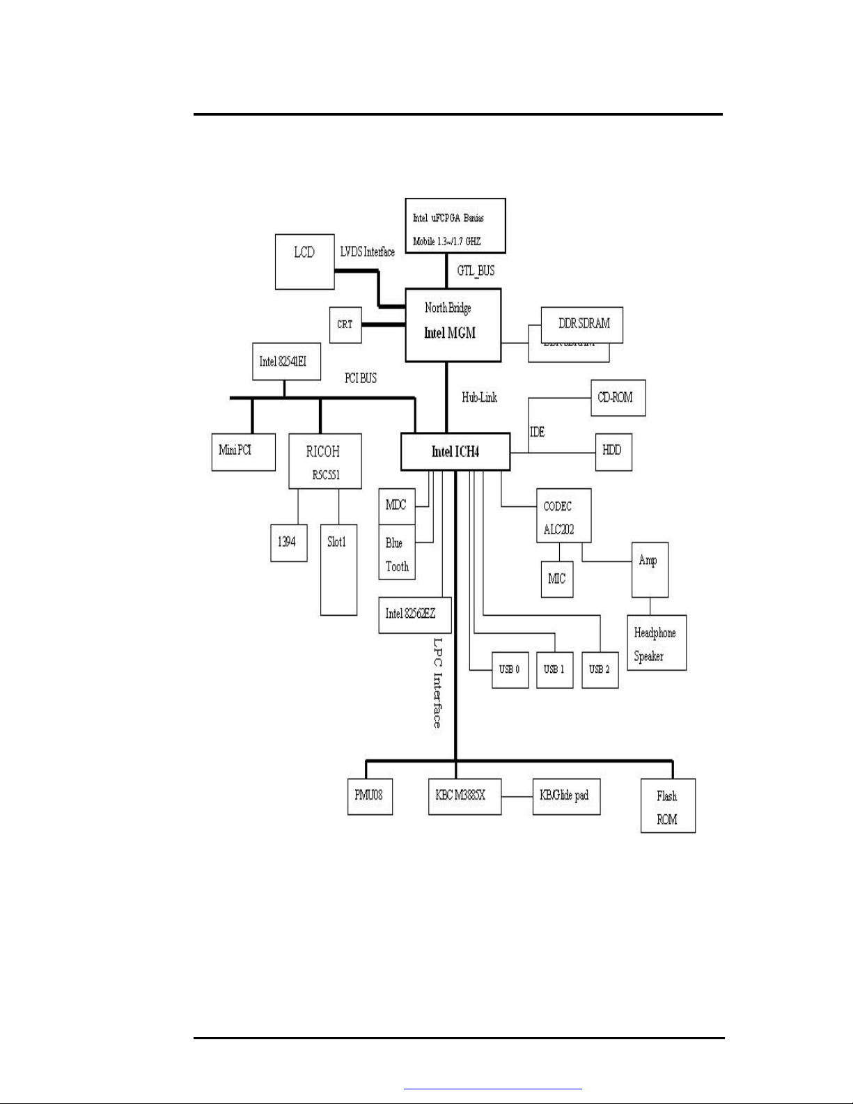
4.2 System Hardware Block Diagram
Figure 1-1 MB02 Block Diagram
FIC MB02 Service Manual 4-5
PDF created with FinePrint pdfFactory trial version http://www.fineprint.com
Page 6
Hardware Functional Overview
4.3 Chipset Summary
The MB02 notebook consists of following major chipsets:
Controller Chip Vendor Description
Processor
North Bridge
South Bridge
Video Controller
PCMCIA Controller
Audio Chip
Audio Codec
Keyboard Controller
PMU Controller
ROM BIOS
Clock Generator
Temperature Sensor
IEE 1394
LAN
Modem
Intel Mobile Banias
Intel MontaraGM
Intel ICH4
Intel Embedded in MontaraGM
RICOH R5C551
Intel South Bridge Integrated
Intel ICH4
Misubishi M3885x
NEC PMU08
SST 49LF004A
IMI CY28346
NS MAX6690
RICOH R5C551
Intel ICH4
Intel MDC AC’97
4.4 System Processor (CPU)
The FIC MB02 runs on Intel Banias based on uFCPGA packaging. It supports CPU with
up to 1.3/1.4/1.5/1.6/1.7 GHZ clock speed rating. The processor operates in conjunction
with the RAM and ROM memory and the system control logic to process software
instructions (BIOS, Windows, and Applications).
Intel Pentium M Features
The Intel® Pentium® M processor is a high performance, low power mobile processor
with several micro-architectural enhancements over existing Intel mobile processors.
The following list provides some of the key features on this processor:
• Supports Intel® Architecture with Dynamic Execution
• High performance, low-power core
• On-die, primary 32-kbyte instruction cache and 32-kbyte write-back data cache
• On-die, 1-MByte second level cache with Advanced Transfer Cache Architecture
• Advanced Branch Prediction and Data Prefetch Logic
• Streaming SIMD Extensions 2 (SSE2)
• 400-MHz, Source-Synchronous processor system bus
• Advanced Power Management features including Enhanced Intel® SpeedStep®
technology
• Micro-FCPGA and Micro-FCBGA packaging technologies
The Intel Pentium M processor is manufactured on Intel’s advanced 0.13 micron process
technology with copper interconnect. The processor maintains support for MMX™
technology and Internet Streaming SIMD instructions and full compatibility with IA-32
software. The high performance core features architectural innovations like Micro-op
Fusion and Advanced Stack Management that reduce the number of micro-ops handled by
the processor. This results in more efficient scheduling and better performance at lower
4-6 FIC MB02 Service Manual
PDF created with FinePrint pdfFactory trial version http://www.fineprint.com
Page 7

Hardware Functional Overview
power. The on-die 32-kB Level 1 instruction and data caches and the 1-MB Level 2 cache
with Advanced Transfer Cache Architecture enable significant performance improvement
over existing mobile processors. The processor also features a very advanced branch
prediction architecture that significantly reduces the number of mispredicted branches. The
processor’s Data Prefetch Logic speculatively fetches data to the L2 cache before an L1
cache requests occurs, resulting in reduced bus cycle penalties and improved performance.
The Streaming SIMD Extensions 2 (SSE2) enable break-through levels of performance in
multimedia applications including 3-D graphics, video decoding/encoding, and speech
recognition.The new packed double-precision floating-point instructions enhance
performance for applications that require greater range and precision, including scientific
and engineering applications and advanced 3-D geometry techniques, such as ray tracing.
The Intel Pentium M processor’s 400-MHz processor system bus utilizes a split-transaction,
deferred reply protocol. The 400-MHz processor system bus uses Source-Synchronous
Transfer (SST) of address and data to improve performance by transferring data four times
per bus clock (4X data transfer rate, as in AGP 4X). Along with the 4X data bus, the
address bus can deliver addresses two times per bus clock and is referred to as a “doubleclocked” or 2X address bus.Working together, the 4X data bus and 2X address bus provide
a data bus bandwidth of up to 3.2 Gbytes/second. The processor system bus uses Advanced
Gunning Transceiver Logic (AGTL+)signal technology, a variant of GTL+ signalling
technology with low power enhancements.
The processor features Enhanced Intel SpeedStep technology, which enables real-time
dynamic switching between multiple voltage and frequency points instead of two points
supported on previous versions of Intel SpeedStep technology. This results in optimal
performance without compromising low power. The processor features the Auto Halt,
Stop-Grant, Deep Sleep, and Deeper Sleep low power states.
The Intel Pentium M processor utilizes socketable Micro Flip-Chip Pin Grid Array (MicroFCPGA) and surface mount Micro Flip-Chip Ball Grid Array (Micro-FCBGA) package
technology. The Micro-FCPGA package plugs into a 479-hole, surface-mount, Zero
Insertion Force (ZIF) socket, which is referred to as the mPGA479M socket.
This document includes specifications for the Intel Pentium M processor at Highest
Frequency Mode (HFM) core frequencies of 1.30, 1.40, 1.50, and 1.60 GHz, the Low
Voltage Intel Pentium M processor at HFM core frequency of 1.10 GHz and the Ultra Low
Voltage Intel Pentium M processor at HFM core frequency of 900 MHz.
4.5 System Core Logic
4.5.1 Intel 852GM Chipset GMCH Features
Processor/Host Bus Support
― Mobile Intel® Pentium® 4 Processor-M (478-pin package)
. Supports the Intel Pentium 4 Processor-M subset of the Enhanced Mode Scalable Bus
Protocol
. 2X Address, 4X data
. Intel Pentium 4 Processor-M System Bus interrupt delivery
. Supports system bus at 400-MHz or 3.2 GB/s
. Supports host Dynamic Bus Inversion (DBI)
. Supports 32-bit host bus addressing
FIC MB02 Service Manual 4-7
PDF created with FinePrint pdfFactory trial version http://www.fineprint.com
Page 8

Hardware Functional Overview
. 12-deep In-Order-Queue
. AGTL+ bus driver technology with integrated AGTL termination resistors (1.3-V
operation)
. Supports Enhanced Intel® SpeedStep® technology
Memory System
. Directly supports one DDR SDRAM channel, 64-bits wide
. Supports 200/266-MHz DDR SDRAM devices with max of 2 Double-Sided SO-DIMMs
(4 rows populated) with unbuffered PC1600/PC2100 DDR SDRAM (without ECC).
. Supports 128-Mbit, 256-Mbit, and 512-Mbit technologies providing maximum capacity
of 1-GB with x16 devices
. All supported devices have 4 banks
. Supports up to 16 simultaneous open pages
. Supports page sizes of 2-kB, 4-kB, 8-kB, and 16-kB. Page size is individually selected for
every row
. UMA support only
System Interrupts
. Supports Intel 8259 and Processor System Bus interrupt delivery mechanism
. Supports interrupts signaled as upstream Memory Writes from PCI and Hub Interface
. MSI sent to the CPU through the System Bus
. From IOxAPIC in ICH4-M
. Provides redirection for upstream interrupts to the System Bus
Hub Interface to ICH4-M
. 266 -MB/s point-to-point Hub Interface to ICH4-M
. 66-MHz base clock
Power Management
. SMRAM space remapping to A0000h (128-kB)
. Supports extended SMRAM space above 256-MB, additional 1-MB TSEG from Top of
Memory,cacheable (cacheability controlled by CPU)
. APM Rev 1.2 compliant power management
. Supports Suspend to System Memory (S3), Suspend to Disk (S4) and Hard Off/Total
Reboot (S5)
. ACPI 1.0b, 2.0 Support
Package
. 732-pin Micro-FCBGA (37.5 x 37.5 mm)
4.5.2 Intel ICH4 Features
The ICH4 provides extensive I/O support. Functions and capabilities include:
•PCI Local Bus Specification, Revision 2.2-compliant with support for 33-MHz PCI
operations.
•PCI slots (supports up to 6 Req/Gnt pairs)
•ACPI Power Management Logic Support
4-8 FIC MB02 Service Manual
PDF created with FinePrint pdfFactory trial version http://www.fineprint.com
Page 9

Hardware Functional Overview
•Enhanced DMA Controller, Interrupt Controller, and Timer Functions
•Integrated IDE controller supports Ultra ATA100/66/33
•USB host interface with support for 6 USB ports; 3 UHCI host controllers; 1 EHCI
high-speed USB 2.0 Host Controller
•Integrated LAN Controller
•System Management Bus (SMBus) Specification, Version 2.0 with additional support
for I2C devices
•Supports Audio Codec ’97, Revision 2.3 specification (a.k.a., AC ’97 Component
Specification, Revision 2.3). Link for Audio and Telephony codecs (up to 7 channels)
•Low Pin Count (LPC) interface
•Firmware Hub (FWH) interface support
•Alert On LAN* (AOL) and Alert On LAN 2* (AOL2)
Hub Architecture
As I/O speeds increase, the demand placed on the PCI bus by the I/O bridge has become
significant. With AC ’97, USB 2.0, and Ultra ATA/100, coupled with the existing USB, I/O
requirements could impact PCI bus performance. The chipset’s hub interface architecture
ensures that the I/O subsystem; both PCI and the integrated I/O features (IDE, AC ‘97,
USB, etc.), receive adequate bandwidth. By placing the I/O bridge on the hub interface
(instead of PCI), the hub architecture ensures that both the I/O functions integrated into the
ICH4 and the PCI peripherals obtain the bandwidth necessary for peak performance.
PCI Interface
The ICH4 PCI interface provides a 33-MHz, Rev. 2.2 compliant implementation. All PCI
signals are 5-V tolerant, except PME#. The ICH4 integrates a PCI arbiter that supports up
to six external PCI bus masters in addition to the internal ICH4 requests.
IDE Interface (Bus Master Capability and Synchronous DMA Mode)
The fast IDE interface supports up to four IDE devices providing an interface for IDE hard
disks and ATAPI devices. Each IDE device can have independent timings. The IDE
interface supports PIO IDE transfers up to 16 Mbytes/sec and Ultra ATA transfers up 100
Mbytes/sec. It does not consume any ISA DMA resources. The IDE interface integrates
16x32-bit buffers for optimal transfers.
The ICH4’s IDE system contains two independent IDE signal channels. They can be
electrically isolated independently. They can be configured to the standard primary and
secondary channels (four devices). There are integrated series resistors on the data and
control lines (see Section 5.15, “IDE Controller (D31:F1)” on page 5-175 for details).
Low Pin Count (LPC) Interface
The ICH4 implements an LPC Interface as described in the LPC 1.0 specification. The
FIC MB02 Service Manual 4-9
PDF created with FinePrint pdfFactory trial version http://www.fineprint.com
Page 10

Hardware Functional Overview
Low Pin Count (LPC) Bridge function of the ICH4 resides in PCI Device 31:Function 0. In
addition to the LPC bridge interface function, D31:F0 contains other functional units
including DMA, Interrupt Controllers, Timers, Power Management, System Management,
GPIO, and RTC.
Note that in the current chipset platform, the Super I/O (SIO) component has migrated to
the Low Pin Count (LPC) interface. Migration to the LPC interface allows for lower cost
Super I/O designs.
Compatibility Modules (DMA Controller, Timer/Counters, Interrupt Controller)
The DMA controller incorporates the logic of two 82C37 DMA controllers, with seven
independently programmable channels. Channels 0–3 are hardwired to 8-bit, count-by-byte
transfers, and channels 5–7 are hardwired to 16-bit, count-by-word transfers. Any two of
the seven DMA channels can be programmed to support fast Type-F transfers.
The ICH4 supports two types of DMA (LPC and PC/PCI). DMA via LPC is similar to ISA
DMA. LPC DMA and PC/PCI DMA use the ICH4’s DMA controller. The PC/PCI
protocol allows PCI-based peripherals to initiate DMA cycles by encoding requests and
grants via two PC/PCI REQ#/GNT# pairs.
LPC DMA is handled through the use of the LDRQ# lines from peripherals and special
encodings on LAD[3:0] from the host. Single, Demand, Verify, and Increment modes are
supported on the LPC interface. Channels 0–3 are 8 bit channels. Channels 5–7 are 16 bit
channels. Channel 4 is reserved as a generic bus master request.
The timer/counter block contains three counters that are equivalent in function to those
found in one 82C54 programmable interval timer. These three counters are combined to
provide the system timer function, and speaker tone. The 14.31818-MHz oscillator input
provides the clock source for these three counters.
The ICH4 provides an ISA-Compatible Programmable Interrupt Controller (PIC) that
incorporates the functionality of two 82C59 interrupt controllers. The two interrupt
controllers are cascaded so that 14 external and two internal interrupts are possible. In
addition, the ICH4 supports a serial interrupt scheme.
All of the registers in these modules can be read and restored. This is required to save and
restore system state after power has been removed and restored to the platform.
Advanced Programmable Interrupt Controller (APIC)
In addition to the standard ISA compatible Programmable Interrupt Controller (PIC)
described in the previous section, the ICH4 incorporates the Advanced Programmable
Interrupt Controller
Universal Serial Bus (USB) Controller
The ICH4 contains an Enhanced Host Controller Interface (EHCI) compliant host ontroller
that supports USB high-speed signaling. High-speed USB 2.0 allows data transfers up to
480 Mb/s which is 40 times faster than full-speed USB. The ICH4 also contains three
Universal Host Controller Interface (UHCI) controllers that support USB full-speed and
4-10 FIC MB02 Service Manual
PDF created with FinePrint pdfFactory trial version http://www.fineprint.com
Page 11

Hardware Functional Overview
low-speed signaling.
The ICH4 supports 6 USB 2.0 ports. All six ports are high-speed, full-speed, and low-
speed capable. ICH4’s port-routing logic determines whether a USB port is controlled by
one of the UHCI controllers or by the EHCI controller. See Section 5.16, “USB UHCI
Controllers (D29:F0, F1 and F2) and Section 5.17, “USB EHCI Controller (D29:F7) for
details.
LAN Controller
The ICH4’s integrated LAN Controller includes a 32-bit PCI controller that provides
enhanced scatter-gather bus mastering capabilities and enables the LAN Controller to
perform high speed data transfers over the PCI bus. Its bus master capabilities enable the
component to process high-level commands and perform multiple operations; this lowers
processor utilization by off-loading communication tasks from the processor. Two large
transmit and receive FIFOs of 3 kB each help prevent data underruns and overruns while
waiting for bus accesses. This enables the integrated LAN Controller to transmit data with
minimum interframe spacing (IFS).
The LAN Controller can operate in either full duplex or half duplex mode. In full duplex
mode the LAN Controller adheres with the IEEE 802.3x Flow Control specification. Half
duplex performance is enhanced by a proprietary collision reduction mechanism. See
Section 5.2, “LAN Controller (B1:D8:F0)” on page 5-78 for details.
RTC
The ICH4 contains a Motorola* MC146818A-compatible real-time clock with 256 bytes of
battery-backed RAM. The real-time clock performs two key functions: keeping track of the
time of day and storing system data, even when the system is powered down. The RTC
operates on a 32.768 KHz crystal and a separate 3-V lithium battery that provides up to
seven years of protection.
The RTC also supports two lockable memory ranges. By setting bits in the configuration
space, two 8-byte ranges can be locked to read and write accesses. This prevents
unauthorized reading of passwords or other system security information.
The RTC also supports a date alarm that allows for scheduling a wake up event up to 30
days in advance, rather than just 24 hours in advance.
4.6 Clock Frequency Generator
The notebook utilizes the IMI CY28346 chip to supply the system clock needed to run the
computer. The following are the available clock frequencies:
System clock:
Clock generator IMI CY28346 support:
- 66/100 MHz for Pentium III Mobile CPU
- 30/33 MHz for PCI device bus clock use
- 48 MHz for PIIX4M
- 14.318 MHz for PIIX4M refresh use
•
14.318 MHz XTAL for Clock Generator use
FIC MB02 Service Manual 4-11
PDF created with FinePrint pdfFactory trial version http://www.fineprint.com
Page 12

Hardware Functional Overview
•
32.768 KHz XTAL for RTC real time clock
• 8.0 MHz XTAL for K/B controller use
• 14.318 MHz OSC for sound blaster use
4.7 Cache Memory
The primary (L1) and secondary (L2) level cache are integrated on the CPU. By
incorporating the cache on-die (meaning it is combined with the CPU into one component),
Intel eliminates the need for separate components. The 512KB on-die L2 cache provides
three (3X) times faster processor access, resulting in significant improvements in
performance. Likewise, an integrated cache means a reduction of connections resulting in
increased reliability.
4.8 System Memory
The memory subsystem, implemented on the motherboard, includes System and Video
memory. The Intel 852GM System Controller chip provides primary control for the system
memory.
4.8.1 System Memory
The notebook offers two 64-bit SODIMM (Small Outline Dual Inline Memory Module)
sockets for main memory configuration. The memory sockets accept any standard 144-pin
SODIMM modules at 128MB, 256MB,512MB and 1GMB sizes. Memory modules are
DDR 200/266 SDRAM type.
4.8.2 Video Memory
The video memory of the notebook is using share system memory with 8~32MB UMA
video memory that can support display resolutions of up to 1024 x 768 at 32-bit 16M color
(TFT LCD).
4.9 System BIOS
The notebook utilizes the Phoenix BIOS 4.0 Release 6.0 (Basic I/O System) that contains
both the main system BIOS and the VGA BIOS with Shadow BIOS capability. It utilizes
Flash EPROM BIOS that allows instant erasing and programming without replacing the
EPROM chip.
The BIOS is stored in a 32-pin PLCC package FLASH ROM SST 49LF040A with 4Mbit
size and is mounted into the motherboard. While posting the system, the Shadow RAM
will be enabled and the ROM will be disabled.
4.10 Video Subsystem
The video subsystem, embedded inside the North Bridge chip and the LCD panel, controls
the display output to both the LCD Panel screen and to the external VGA port.
4.10.1 Video Chip Controller
Features summary of the Intel 852GM Video Chip Controller:
Video Stream Decoder
4-12 FIC MB02 Service Manual
PDF created with FinePrint pdfFactory trial version http://www.fineprint.com
Page 13

Hardware Functional Overview
. Improved HW Motion Compensation for MPEG2
. All format decoder (18 ATSC formats) supported
. Dynamic Bob and Weave support for Video Streams
. Software DVD at 60 fields/second and 30 frames/second full screen
. Support for standard definition DVD (i.e. NTSC pixel resolution of 720x480, etc.) quality
encoding at low CPU utilization
Video Overlay
. Single high quality scalable Overlay and second Sprite to support second Overlay
. Multiple Overlay functionality provided via Arithmetic Stretch Blt
. 5-tap horizontal, 3-tap vertical filtered scaling
. Multiple Overlay formats
. Direct YUV from Overlay to TV-out
. Independent Gamma Correction
. Independent Brightness / Contrast/ Saturation
. Independent Tint/Hue support
. Destination Colorkeying
. Source Chromakeying
Multiple hardware color cursor support (32-bit with alpha and legacy 2-bpp mode)
Accompanying I2C and DDC channels provided through multiplexed interface
Display
. Analog Display Support
. 350-MHz integrated 24-bit RAMDAC that can drive a standard progressive scan analog
monitor with pixel resolution up to 1600x1200 at 85-Hz and up to 1920x1440 at 60 Hz
. Dual independent pipe support
‧ Concurrent: Different images and native display timings on each display device
‧ Simultaneous: Same images and native display timings on each display device
. DVO (DVOC) support
‧ Digital video out port DVOC with 165-MHz dot clock on 12-bit double pumped
interface
‧ Variety of DVO devices supported
‧ Compliant with DVI Specification 1.0, thereby providing support for a display
resolution up to 1400x1050 @ 75-Hz, up to 1600x1200 at 60-Hz, or up to 1920x1200 @
60 Hz
. Dedicated LFP (local flat panel) LVDS interface
‧ Single or dual channel LVDS panel support up to SXGA+(1400x1050 @ 60 Hz) panel
resolution with frequency range from 25-MHz to 112-MHz (single channel/dual channel)
‧ SSC support of 0.5%, 1.0%, and 2.5% center and down spread with external SSC clock
‧ Supports data format of 18-bpp
‧ LCD panel power sequencing compliant with SPWG timing specification
‧ Compliant with ANSI/TIA/EIA –644-1995 spec
‧
Integrated PWM interface for LCD backlight inverter control
‧ Bi-linear Panel fitting
. Tri-view support through LFP interface, DVO C port, and CRT Internal Graphics
Features
. Up to 64 MB of Dynamic Video Memory Allocation
. Display Image Rotation
. Core Frequency
‧ Display Core frequency of 133-MHz
FIC MB02 Service Manual 4-13
PDF created with FinePrint pdfFactory trial version http://www.fineprint.com
Page 14

Hardware Functional Overview
‧ Render Core frequency of 133-MHz
.
2D Graphics Engine
‧ Optimized 128-bit BLT engine
‧ Ten programmable and predefined monochrome patterns
‧ Alpha Stretch Blt (via 3D pipeline)
‧ Anti-aliased lines
‧ Hardware-based BLT Clipping and Scissoring
‧ 32-bit Alpha Blended cursor
‧
Programmable 64 x 64 3-color Transparent cursor
‧ Color Space Conversion
‧ 3 Operand Raster BLTs
‧ 8-bit, 16-bit, and 32-bit color
‧ ROP support
‧ DIB translation and Linear/Tile addressing
.
3D Graphics Engine
‧ 3D Setup and Render Engine
‧ Viewpoint Transform and Perspective Divide
‧ Triangle Lists, Strips and Fans support
‧ Indexed Vertex and Flexible Vertex formats
‧ Pixel accurate Fast Scissoring and Clipping operation
‧ Backface Culling support
‧ DirectX* and OGL Pixelization rules
‧ Anti-Aliased Lines support
‧ Sprite Points support
‧ Provides the highest sustained fill rate performance in 32-bit color and 24-bit W mode
‧
High quality performance Texture Engine
‧ 266-MegaTexel/s peak performance
‧ Per Pixel Perspective Corrected Texture Mapping
‧ Single Pass Texture Compositing (Multi-Textures) at rate
‧ Enhanced Texture Blending functions
‧ Twelve Level of Detail MIP Map Sizes from 1x1 to 2Kx2K
‧ Numerous Texture formats including 32-bit RGBA
‧ Alpha and Luminance Maps
‧ Texture Chromakeying
‧ Bilinear, Trilinear, and Anisotropic MIP - Mapped Filtering
‧ Cubic Environment Reflection Mapping
‧ Embossed Bump-Mapping
‧ DXTn Texture Decompression
‧ FX1 Texture Compression
‧ 3D Graphics Rasterization enhancements
‧ One Pixel per clock
‧ Flat and Gouraud Shading
‧ Color Alpha Blending for Transparency
‧ Vertex and Programmable Pixel Fog and Atmospheric effects
4-14 FIC MB02 Service Manual
PDF created with FinePrint pdfFactory trial version http://www.fineprint.com
Page 15

Hardware Functional Overview
‧ Color Specular Lighting
‧ Z Bias support
‧ Dithering
‧ Line and Full-Scene Anti-Aliasing
‧ 16 and 24-bit Z Buffering
‧ 16 and 24-bit W Buffering
‧ 8-bit Stencil Buffering
‧ Double and Triple Render Buffer support
‧ 16 and 32-bit color
‧ Destination Alpha
‧ Vertex Cache
‧ Maximum 3D resolution of 1600x1200 at 85- Hz (contact your Intel Field
Representative for detailed display information, i.e. pixel depths, etc.)
‧ Optimal 3D resolution supported
‧ Fast Clear support
‧ ROP support
4.10.2 Video Clock
Intel 852GM North Bridge provides input to generate VGA internal slate machine, MCLK,
and DCLK. Also provides 32.768 KHz O/P for video RAM refresh.
4.11 PCMCIA Controller
The PCMCIA controller of the notebook is implemented on the motherboard using the
RICOH R5C551 CardBus Controller. The MB02 notebook only supports single PCMCIA
slot for PCI-Cardbus Bridge.
CARDBUS CONTROLLERS
The R5C551 is an ACPI and PC98/99 logo certified high performance, single slot PC Card
controller with a synchronous 32-bit bus master/target PCI interface. This PC Card to PCI
bridge host controller is compliant with the 2000 PC Card Standard. This standard
incorporates the new 32-bit CardBus while retaining the 16-bit PC Card specification as
defined by PCMCIA release 2.1. CardBus is intended to support "temporal" add-in
functions on PC Cards, such as Memory cards, Network interfaces, FAX/Modems and
other wireless communication cards, etc. The high performance and capability of the
CardBus interface will enable the new development of many new functions and
applications.
The R5C551 CardBus controller is compliant with the latest ACPI-PCI Bus Power
Management interface Specification. It supports all four power states and the PME#
function for maximum power savings and ACPI compliance. Additional compliance to On
Now Power Management includes D3 cold state support, paving the way for low sleep
state power consumption and minimized resume times. To allow host software to reduce
power consumption further, the R5C551 provides a power-down mode in which internal
clock distribution and the PC Card socket clocks are stopped. An advanced CMOS process
is also used to minimize system power consumption.
The R5C551 single PCMCIA socket supports the 3.3V/5V 8/16-bit PC Card R2 cards or
FIC MB02 Service Manual 4-15
PDF created with FinePrint pdfFactory trial version http://www.fineprint.com
Page 16

Hardware Functional Overview
32-bit CardBus R3 cards. The R2 card support is compatible with the Intel 82365SL PCIC
controller, and the R3 card support is fully compliant with the 2000 PC Card Standard
CardBus specification. The R5C551 is an additional buffer chip for the PC Card socket
interface. In addition, the R5C551 supports dynamic PC Card hot insertion and removal,
with auto configuration capabilities.
The R5C551 is fully complains with the 33Mhz PCI Bus specification, v2.2. It supports a
master device with internal CardBus direct data transfer. The R5C551 implements FIFO
data buffer architecture between the PCI bus and CardBus socket interface to enhance data
transfers to CardBus Devices. The bi-directional FIFO buffer permits the R5C551 to
accept data from a target bus (PCI or CardBus interface) while simultaneously transferring
data. This architecture not only speeds up data transfers but also prevents system deadlocks.
The R5C551 is a PCMCIA R2/CardBus controller, providing the most advanced design
flexibility for PC Cards that interface with advanced notebook designs.
R5C551 FEATURES – Slot Solution
• Supports only one PCMCIA 2.1 and JEIDA 4.2 R2 cards or 2 CardBus cards
• ACPI-PCI Bus Power Management Interface Specification Rev 1.1 Compliant
• Supports OnNow LAN wakeup, OnNow Ring Indicate, PCI CLKRUN#, PME#,
and CardBus CCLKRUN#
• Compliant with the 33Mhz PCI Specification V2.2, 2000 PC Card Standard 7.1 for
R5C551
• Yenta™ PCI to PCMCIA CardBus Bridge register compatible
• ExCA (Exchangeable Card Architecture) compatible registers map-able in
memory and I/O space
• Intel™ 82365SL PCIC Register Compatible
• Supports PCMCIA_ATA Specification
• Supports 5V/3.3V PC and 3.3V Cardbus cards
• Supports two PC Card or CardBus slots with hot insertion and removal
• Supports multiple FIFOs for PCI/CardBus data transfer
• Supports Direct Memory Access for PC/PCI and PCI/Way on PC Card socket
• Programmable interrupt protocol: PCI, PCI+ISA, PCI/Way, or PC/PCI interrupt
signaling modes
• Win'98 IRQ and PC-98/99 compliant
• Parallel or Serial interface for socket power control devices including Micrel and
TI
• Integrated PC 98/99 -Subsystem Vendor ID support, with auto lock bit
4-16 FIC MB02 Service Manual
PDF created with FinePrint pdfFactory trial version http://www.fineprint.com
Page 17

Hardware Functional Overview
• LED Activity Pins
• R5C551 supports D3cold state PME# wakeup; 3.3Vaux Power; and Zoomed video
buffer enable pins
• R5C551: "Built-in" live video, high throughput, multimedia ZV ports support
without additional buffers; 3V card protection during host system suspend with
Auto Card VS# resensing; dedicated ZV output port to LCD controller
SmartCardBus™ combines a Smart Card reader and CardBus controller in a single IC. In
addition to meeting PC Card standards, SmartCardBus is compliant to Microsoft PC/SC,
ISO 7816-1, -2, -3 electrical specifications, standard protocols including T = 0, T = 1, and
synchronous and asynchronous formats. SmartCardBus lowers the cost of ownership of ecommerce and corporate security Smart Card applications.
4.12 Audio Subsystem
The audio subsystem is integrated inside the South Bridge chip on the motherboard. Refer
to the System Core Logic section of this chapter.
An internal two-way mini speaker and microphone provide the notebook with mobile
sound generation and recording capabilities. In addition, a set of 3.5mm bayonet socket
(1/8” minijack) connectors allow for external microphone, line inputs, and headphone
outputs.
4.13 Keyboard and Pointing Device
The Keyboard Subsystem of the notebook is implemented on the Motherboard and
Keyboard Assembly using the Mitsubishi M38859 keyboard controller chip and the
Mitsubishi M38859 keyboard controller firmware. This chip controls the internal built-in
keyboard, the built-in touchpad pointing device, as well as the external PS/2 keyboard and
mouse port. The keyboard controller allows simultaneous use of both the internal and
external keyboard and PS/2 mouse.
The MB02 membrane keyboard is an 86-key IBM 101-key enhanced compatible keyboard
with standard characters and 12 function keys including an embedded numeric keypad. See
Chapter 1 for more information.
The pointing device subsystem consists of the built-in Synaptics touch pad pointing device
module on the system top cover assembly and a pre-programmed Mitsubishi M38859
micro-controller that interfaces the mouse device to the Motherboard. The touch pad
module is connected to battery board through a 6-pin FPC cable. An external PS/2 port
also supports the use of an external PS/2 compatible mouse where the system
automatically detects on system power up and runs both internal and external mouse
simultaneously.
FIC MB02 Service Manual 4-17
PDF created with FinePrint pdfFactory trial version http://www.fineprint.com
Page 18

Hardware Functional Overview
The Synaptic touch pad, a pointing device for personal computers, detects the position of a
finger over a touch-sensitive area. To move the cursor, the user lightly slides a finger over
the smooth sensor area. To ‘click’, the user gently taps on the surface.
The ultra-thin module is the thinnest PCB based touchpad available today. It is a capacitive
sensor - the finger is detected by measuring its effect on an array of capacitive lines
integrated into the PC board. The pad senses both the finger’s position and its contact area
(X, Y, and Z). The area of contact is a measure of applied pressure. One side of the module
PC board is the sensor surface; electronic components are mounted on the other side. The
sensitive area is protected by a layer of smooth and durable mylar.
The Synaptic touch pad communicates with the host via a standard PS/2 mouse or trackball
interface. It is fully compatible with the standard Microsoft mouse driver. The module
connector includes the PS/2 signal pins, power supply pins and two connections for
external button switches.
The Synaptic touch pad includes a special “edge-motion” feature that allows the user to
extend a drag operation when the finger reaches the edge of the sensor pad. The cursor
continues to coast in the indicated direction when the finger is held against the edge.
4.14 Disk Drives Subsystem
The disk drives subsystem, implemented on the Motherboard and on the associated internal
hard disk drive assembly and device bay, provides disk storage for all system software and
user files.
The notebook is equipped with high capacity hard disk drive using Enhanced IDE
controller with LBA (Logical Block Addressing) and Ultra DMA mode support.
The ICH4 controller chip provides the Primary IDE controller for the internal hard disk,
and the Secondary Master for the CD-ROM.
The notebook uses the 24X-speed IDE CD-ROM Drive that reads digital data stored on
CD-ROM at 24 times faster rotational speed. The CD-ROM drive supports CD-DA
transfer over ATAPI function that the host system can read CD audio data. The drive also
supports Photo-CD Multi-session disc compatibility and Multimedia PC-3 specification
compatibility. The notebook also could use the 8X+ speed IDE DVD-ROM Drive that
reads DVD digital data stored on DVD-ROM at 8 times faster rotational speed.
4.15 Power Subsystem
The Power Subsystem consists of the following major sections:
4.15.1 AC Power Adapter
The computer is equipped with a 60W Peak 80W universal AC power adapter that converts
AC voltage (100 to 240VAC, 50 to 60Hz) into DC voltage used to operate the notebook
and charge the batteries.
4-18 FIC MB02 Service Manual
PDF created with FinePrint pdfFactory trial version http://www.fineprint.com
Page 19

Hardware Functional Overview
4.15.2 Internal Battery Pack
The computer utilizes Lithium-Ion (Li-Ion) that provides DC power for the notebook and
real time clock battery on the motherboard when the AC Adapter is not connected to the
computer.
The normal charging time for the battery is around 3.5 hours when computer is turn off
while it should take around 8 hours when the computer is running. Running time of battery
is around 4.5 hours.
4.15.3 DC-DC Module of Motherboard
The DC-DC module receives approximately 12VDC from the battery pack and uses this
input voltage to generate multiple regulated output voltages to provide power for all
internal notebook board assemblies.
4.15.4 LCD Inverter Board Assembly
The LCD Inverter Board Assembly is located in the LCD Panel Assembly. It converts the
+12VDC input directly from the Battery Pack into a high voltage AC output used to light
the CCFT (Cold-Cathode Fluorescent Tube).
4.16 Micro- P Subsystem (PMU-08)
The micro controller NEC PMU08 acts as a supplement for the power management control.
It supports many functions via the SMBus interface.
The system communicates with the PMU08 via the SMBus interface. The SMBus host
should be first initialized before starting the transaction. The following is the procedure for
system communication with PMU08:
1. Enable SMBus interface by writing 01h to SmbHstCfg register.
2. Get SMBus I/O port base address by reading from SmbBA register.
3. Clear SMBus status by writing 1Eh to SmbHstSts register.
4. Write the PMU07 slave address to SmbHstAdd register.
− Send command to PMU08 -- Slave address is 04h.
−
Read data from PMU08 -- Slave address is 05h.
5. Write the desired command to SmbHstCmd register.
6. Write the desired parameters to SmbHstDat0 (High byte) and SmbHstDat1 (Low
byte) registers if the system wants to send command to PMU08.
7. Wait for SMBus interrupt occurred by monitoring SmbHstSts register INTR bit.
8. Get the desired data by reading from SmbHstDat0 (High byte) and SmbHstDat1
(Low byte) registers if the system wants to read data from PMU08.
Features Summary of the Micro-P:
• 5 channels 8-bit analog to digital converter
•
Timer0: 8-bit tuner/counter with 8-bit prescaler
• Timer1: 16-bit timer/counter. TMR1 can be incremented during sleep via external
crystal/clock
• Timer2: 8-bit timer/counter with 8-bit period register, prescaler and postscaler
• Capture, Compare, PWM module
FIC MB02 Service Manual 4-19
PDF created with FinePrint pdfFactory trial version http://www.fineprint.com
Page 20

Hardware Functional Overview
• Synchronous Serial port (SSP) with SPI and I2C
• Universal Synchronous Asynchronous Receiver Transmitter (USART/SCI)
•
Brown-out detection circuitry for Brown-out Reset (BOR)
• 2K bytes program memory
• 128 bytes data memory
• 22 I/O pin
•
8 interrupt sources
4-20 FIC MB02 Service Manual
PDF created with FinePrint pdfFactory trial version http://www.fineprint.com
 Loading...