

Page 1

sync
sync pulse
Appendix
Pin Assignments
B.1 CRT (VGA) Connector
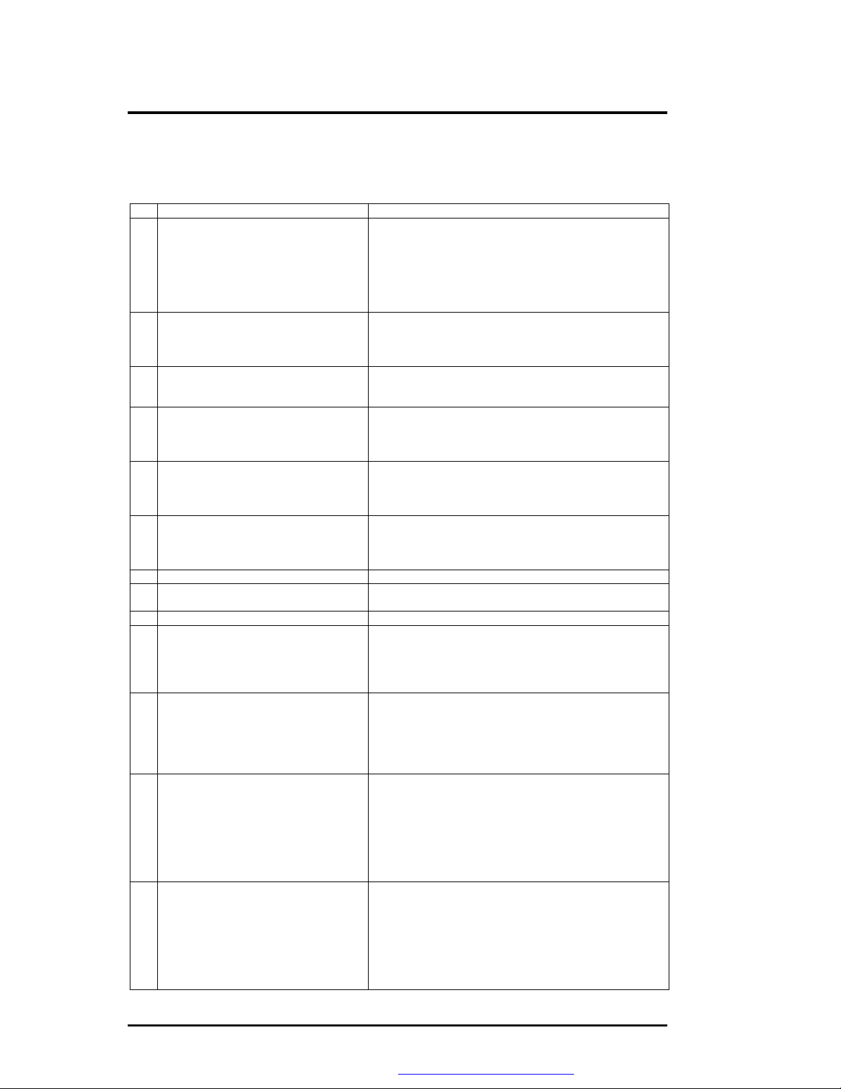
The pin assignment of the VGA connector is as follows:
No
PIN ASSIGEMENT(by: sort) DESCRIPTION
1 RED Video_5 :O (analog) Red this DAC analog output drives the CRT interface.
2 GREEN Video_5 :O (analog) Green this DAC analog output drives the CRT interface.
3 BLUE Video_5 :O (analog) Blue this DAC analog output drives the CRT interface.
4 Monitor ID Bit 2 : Option
5 GROUND : Ground
6 RED Return (ground) : Ground
7 GREEN Return (ground) : Ground
8 BLUE Return (ground) : Ground
9 KEY (no connector) : VCC
10 SYNC Return (ground) :
11 MONITOR ID Bit 0_5 : Monitor Sense Indicator
12 MONITOR ID Bit 1_5 :I DDC monitor data
13 HORIZONTAL SYNC_5 :O (t/s)
14 VERTICAL SYNC_5 :O (t/s)
15 MONITOR ID Bit 3_5 :I/O DDC monitor clock
Absolute Maximum Conditions
Below parameters are maximum ratings for VGA. Permanent device damage may occur if
these rating are exceeded. Extended exposure to these ratings may also cause device failure.
PARAMETER MIN MAX UNIT
I/O VOLTAGE -0.5 +6.00V V
OUTPUT CURRENT
B.2 Serial Port Connector
The pin assignment of the serial (COM1) port connector is as follows:
No PIN ASSIGMENT (by: sort)
1 DCDA#_T:I Active low Data Carrier Detect inputs for the serial port.
2 SINA_T:I Receiver serial data input for port 1.
3 SOUTA_12:O Transmit serial data output for port 1.
4 DTRA#_6:O Active low Data Terminal Ready outputs for the serial port.
5 GND Ground
6 DSRA#_T:I Active low Data Set Ready inputs for the serial port.
7 RTSA#_6:O Active low Request to Send Outputs for the serial port.
8 CTSA#_T:I Active low Clear to Send inputs for the serial port.
9 RI#_T:I Active low Ring Indicator inputs for the serial port.
Ground
CRT Horizontal Sync this output is The Horizontal
pulse for the CRT Monitor.
CRT Vertical Sync this output is the Vertical
for the CRT Monitor.
-12mA(source)
+24mA(sink)
DESCRIPTION
m A
FIC A985 Service Manual B-1
PDF created with FinePrint pdfFactory trial version http://www.fineprint.com
Page 2
An active low pulse on this output is used to strobe the
The STROBE output is the complement of Bit 0 of the
f this pin in ECP
This active low Schmidt trigger input senses from the disk
drive that the head is positioned over the beginning of a
This active low Schmidt trigger input senses from the disk
4
This active low Schmidt trigger input senses from the disk
Each falling edge represents a flux transition of the
This input senses that the driver door is open or that the
diskette has possibly been changed since the last drive
A low active output from the printer indicating that it has
of this pin in ECP
This is a status output from the printer, a high indicating
Bit 7 of the Printer status register is the complement Of
arallel port description for use
Another status output from the printer, a high indicating
egister reads the PE input.
Refer to parallel port description for use of this pin in ECP
This active low high current driver provide the encoded
This high active output from the printer indicates that it
Refer to parallel port description for use of this pin in ECP
lows current to flow
Pin Assignments
B.3 Parallel Port Connector
The pin assignment of the parallel/printer (LPT1) port connector is as follows:
No
1 STB#/DS0#_D14/_P14/_D12:O
2 PD0/INDEX3#_P14/_S:IO/I Port data 0
3 PD1/TRK0#_P14/_S:IO/I Port data 1
5 PD3/RDATA#_P14/_S:IO/I Port data 3
PIN ASSIGMENT(by: sort) Description
printer data into the printer.
printer control register.
Refer to parallel port description for use o
and EPP mode.
Active low outputs select driver 0
track as marked by an index hole.
drive that the head is positioned over the outermost track.
PD2/WRTPRT#_P14/_S:IO/I Port data 2
drive that a disk is write protected.
Any write command is ignored.
Raw serial bit stream from the disk drive, low active.
encoded data.
6 PD4/DSKCHG_P14/_S:IO/I Port data 4
selection.
7 PD5_P14:IO Port data 5
8 PD6/MTR0#_P14/_D12:IO/O Port data 6
9 PD7_P14:IO Port data 7
10 ACK#/DS1#_T_D12:I/O
11 BUSY/MRT1#_T/_D12:_I/O
12 PE/WDATA#_T/_D12:I/O
13 SLCT/WGATE#_T/_D12:I/O
This active low outputs select motor drives 0.
received the data and is ready to accept new data.
Bit 6 of the printer status register reads the ACK# Input.
Refer to parallel port description for use
and EPP mode.
that the printer is not ready to receive new data.
the BUSY input. Refer to p
of this pin in ECP and EPP mode.
This active low outputs select motor Drives 1.
that printer is out of paper.
Bit 5 of the printer status r
and EPP mode.
data to the disk drive.
Each falling edge cause a flux transfer on the media.
has power on.
Bit 4 of the printer status register read the SLCT input.
and EPP mode.
This active low high current driver al
through the write head.
It become active just prior to writing to the diskette.
B-2 FIC A985 Service Manual
PDF created with FinePrint pdfFactory trial version http://www.fineprint.com
Page 3
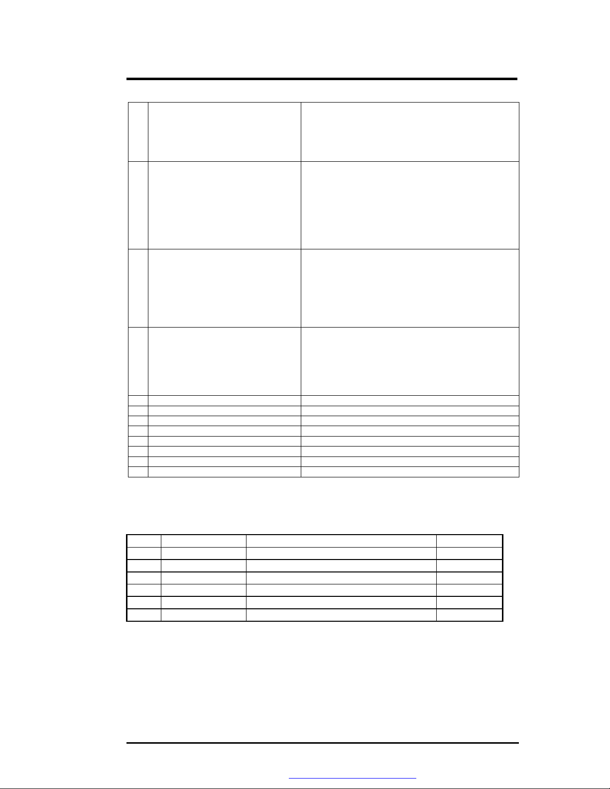
This output goes low to cause the printer to automatically
he complement of bit 1 of the printer
Refer to parallel pot description for use of this pin in ECP
A low on this input from the printer indicates that there is
Refer to parallel port description for use of this pin in ECP
This high current output selects the floppy disk side for
ccessed
This output is bit 2 of the printer control register. This is
Refer to parallel port description for use of this pin in ECP
This high current low active output determines the
A logic “1” on this pin means outward motion, while a
This is the complement of bit 3 of the printer control
Refer to parallel port description for use of this pin in ECP
This active low high current driver issues s low pulse for
Pin Assignments
14 AFD#/DSB#_D14,_P14/_D12:O,O/O
15 ERR#/HDSEL_T/D12:I/O
16 INIT#/DIR#_D14,_P14/D12:O,O/O
17 SLIN#/STEP#_D14,_P14/_D12:O,O/O This active low output selects the printer.
18 GND: Ground
19 GND: Ground
20 GND: Ground
21 GND: Ground
22 GND: Ground
23 GND: Ground
24 GND: Ground
25 GND: Ground
feed one line after each line is printed.
The AFD# output is t
control register.
and EPP mode.
a error condition at the printer.
Bit 3 of the printer status register reads the ERR# input.
and EPP mode.
reading or writing.
A logic “1” on this pin means side 0 will be a
while a logic “0” means side 1 will be acessed.
used to initiate the printer when low.
and EPP mode.
direction of the head movement.
logic “0” means inward motion.
register.
and EPP mode.
each track to track movement of the head.
B.4 PS/2 Mouse / Ext. Keyboard Mini-DIN Connector
Following is the pin assignment of the PS/2 connector:
No Signal Description Type
1 MOUSE_CLK External clock for mouse or keyboard I/O
2 EKB_CLK External clock for mouse or keyboard I/O
3 +5vs 5v power supply O
4 Gnd Ground I
5 EKB_DATA External data for mouse or keyboard I/O
6 MOUSE_DATA External data for mouse or keyboard I/O
FIC A985 Service Manual B-3
PDF created with FinePrint pdfFactory trial version http://www.fineprint.com
Page 4

Pin Assignments
B.5 USB Connector
The pin assignment of the USB port connector is as follows:
No Signal Description Type
1, 5, 9, 10, 11, 12
2 USBP0+ USB port0 bus signal O
3 USBP0- USB port0 bus signal O
4 +5VS USB port0 power
6 USBP1+ USB port1 bus signal
7 USBP1- USB port1 bus signal
8 +5VS USB port1 power
B.6 CD-ROM IDE Connector
The following is the pin assignment for the CD-ROM IDE connector:
NO. Signal Description Type
5 CDROMRESET# Reset secondary disk O
33 RSDA0 Secondary disk address 0 O
31 RSDA1 Secondary disk address 1 O
34 RSDA2 Secondary disk address 2 O
21 RSDD0 Secondary disk data 0 I/O
19 RSDD1 Secondary disk data 1 I/O
17 RSDD2 Secondary disk data 2 I/O
15 RSDD3 Secondary disk data 3 I/O
13 RSDD4 Secondary disk data 4 I/O
11 RSDD5 Secondary disk data 5 I/O
9 RSDD6 Secondary disk data 6 I/O
7 RSDD7 Secondary disk data 7 I/O
6 RSDD8 Secondary disk data 8 I/O
8 RSDD9 Secondary disk data 9 I/O
10 RSDD10 Secondary disk data 10 I/O
12 RSDD11 Secondary disk data 11 I/O
14 RSDD12 Secondary disk data 12 I/O
16 RSDD13 Secondary disk data 13 I/O
18 RSDD14 Secondary disk data 14 I/O
20 RSDD15 Secondary disk data 15 I/O
35 RSDCS1# Secondary disk chip select for 100 range O
36 RSDCS3# Secondary disk chip select for 300 range O
28 RSDDACK# Secondary DMA acknowledge O
22 RSDDREQ Secondary DMA request I
24 RSDIOR# Secondary disk IO read O
25 RSDIOW# Secondary disk IO write O
27 RSIORDY Secondary disk IO channel ready I
29 IRQ15 Secondary disk interrupt I
50 NC NC
49 NC NC
37 CDROMLED# CDROM access indicator O
2 CD_R CDROM sound right signal O
4 GND Ground I
1 CD_L CDROM sound left signal O
3 CD_RGND Left Ground I
39,41,38,40,42 +5Vs +5V power supply I
23,43,44,45,46,48
47 CSEL SELECT MASTER OR SLAVE I
GND Ground O
Gnd Ground O
B-4 FIC A985 Service Manual
PDF created with FinePrint pdfFactory trial version http://www.fineprint.com
Page 5

Flat panel backlight signal
Pin Assignments
B.7 DC-IN Jack Pin Assignment
The pin assignment of the DC-IN connector is as follows:
No Signal Description Type
1 ADAPV+ Adapter input voltage I
2 Gnd Ground O
B.8 LCD Connector Pin Assignment
The pin assignment of the LCD connector is as follows:
NO. Signal Description Type
22 INVENA
2 LCDID0 LCD type bit0 I
4 LCDID1 LCD type bit1 I
6 LCDID2 LCD type bit2 I
8 LCDID3 LCD type bit3
20 BRIGHTNESS LCD brightness adjust voltage O
23 TXOUTU0- O
21 TXOUTU0+ O
17 TXOUTU1- O
15 TXOUTU1+ O
11 TXOUTU2- O
9 TXOUTU2+ O
5 TXCLK- O
3 TXCLK+ O
16 MAIL LED
10 LED GREEN
12 LED AMBER
14 LED CHG
46,48,50 +3V
24,26,28,30,32 +5V
1,7,13,19,25,31,37,43,49,34,36,38,
40,42,44
18 NC
GND
control the LCD backlight.
B.9 HDD Pin Assignment
The pin assignment of the internal HDD is as follows:
NO. Signal Description Type
1 HDDRESET# Reset primary disk O
35 RPDA0 Primary disk address 0 O
33 RPDA1 Primary disk address 1 O
36 RPDA2 Primary disk address 2 O
17 RPDD0 Primary disk data 0 I/O
15 RPDD1 Primary disk data 1 I/O
13 RPDD2 Primary disk data 2 I/O
11 RPDD3 Primary disk data 3 I/O
9 RPDD4 Primary disk data 4 I/O
7 RPDD5 Primary disk data 5 I/O
5 RPDD6 Primary disk data 6 I/O
O
FIC A985 Service Manual B-5
PDF created with FinePrint pdfFactory trial version http://www.fineprint.com
Page 6

Pin Assignments
3 RPDD7 Primary disk data 7 I/O
4 RPDD8 Primary disk data 8 I/O
6 RPDD9 Primary disk data 9 I/O
8 RPDD10 Primary disk data 10 I/O
10 RPDD11 Primary disk data 11 I/O
12 RPDD12 Primary disk data 12 I/O
14 RPDD13 Primary disk data 13 I/O
16 RPDD14 Primary disk data 14 I/O
18 RPDD15 Primary disk data 15 I/O
37 RPDCS1# Primary disk chip select for 100 range O
38 RPDCS3# Primary disk chip select for 300 range O
29 RPDDACK# Primary DMA acknowledge O
21 RPDDREQ Primary DMA request I
25 RPDIOR# Primary disk IO read O
23 RPDIOW# Primary disk IO write O
27 RPIORDY Primary disk IO channel ready I
31 IRQ14 Primary disk interrupt I
39 HDDLED# HDD access indicator O
2,19,22,24,26
,28,3040,43
41,42 +5Vs +5v power supply O
Gnd
B.10 Internal Keyboard FPC Connector
The pin assignment of the internal keyboard connector is as follows:
No Signal Description Type
1,25 X15 Keyboard matrix column 15 I
2,26 X14 Keyboard matrix column 14 I
3,27 X13 Keyboard matrix column 13 I
4,28 X12 Keyboard matrix column 12 I
5,29 X11 Keyboard matrix column 11 I
6,30 X10 Keyboard matrix column 10 I
7,31 X9 Keyboard matrix column 9 I
8,32 X8 Keyboard matrix column 8 I
9,33 X7 Keyboard matrix column 7 I
10,34
11,35
12,36
13,37
14,38
15,39
16,40
17,41
18,42
19,43
20,44
21,45
22,46
23,47
24,48
X6 Keyboard matrix column 6 I
X5 Keyboard matrix column 5 I
XY7 Keyboard matrix row 7 O
XY6 Keyboard matrix row 6 O
XY5 Keyboard matrix row 5 O
XY4 Keyboard matrix row 4 O
X4 Keyboard matrix column 4 I
X3 Keyboard matrix column 3 I
XY3 Keyboard matrix row 3 O
XY2 Keyboard matrix row 2 O
XY1 Keyboard matrix row 1 O
XY0 Keyboard matrix row 0 O
X2 Keyboard matrix column 2 I
X1 Keyboard matrix column 1 I
X0 Keyboard matrix column 0 I
Ground
I
B-6 FIC A985 Service Manual
PDF created with FinePrint pdfFactory trial version http://www.fineprint.com
Page 7

Pin Assignments
B.11 Battery Connector
The pin assignment for the battery connector is as follows:
No Signal Description Type
1 Gnd Ground 2 B_PMU5V I
3 BAT+ Battery output/input voltage I/O
4 CLK SMBus clock signal I/O
5 DTA SMBus data signal I/O
6 TH1 THERMAL O
7 BIN1 O
8 GND GROUND -
B.12 Audio Jack
The audio jack comprises of the headphone jack, line-out jack, and microphone jack:
SPDIF & Headphone Jack
The pin assignment of the headphone jack is as follows:
No Signal Description Type
4 GND Ground I
2 HP_L Headphone left sound O
3 HP_R Headphone right sound O
5 SPDIFDET SPDIF insert detect I
1 HPDET Headphone insert detect I
8 SPDIF PWR SPDIF power O
7 SPDIF SPDIF signal O
9 GND Ground I
Microphone Jack
The pin assignment of the microphone jack is as follows:
No Signal Description Type
1 GND Ground I
2 MICIN External Microphone input signal I
3 GND Ground I
4 EXTMICDET EXTERNAL MIC detect I
5 GND Ground I
B.13 Internal Microphone Connector
The pin assignment of the internal microphone is as follows:
No Signal Description Type
1 MICIN External Microphone input signal
2 GND Ground
FIC A985 Service Manual B-7
PDF created with FinePrint pdfFactory trial version http://www.fineprint.com
 Loading...