


RTS2
Suite 6, Cookson House,
River Drive, South Shields,
Tyne & Wear. Tel: (091) 427 7774
NE33 1IX England Fax: (091) 427 5566

CONTENTS Page
1. TECHNICAL SPECIFICATION 1
1.1 Oscillator 1
1.2 Wow & Flutter Oscillator 1
1.3 Millivoltmeter 1
1.4 Wow & Flutter Meter 2
1.5 Distortion Meter 2
1.6 General 3
2. OPERATING INSTRUCTIONS 4
2.1 Connections 4
2.1.1 Power Supply 4
2.1.2 Signal 4
2.2 Calibration 4
2.2.1 General 4
2.2.2 Millivoltmeter 5
2.2.3 Drift 5
2.2.4 Wow & Flutter 5
2.3 Measurements 6
2.3.1 Preparation 6
2.3.2 Frequency Response 6
2.3.3 Drift 7
2.3.4 Wow & Flutter 8
2.3.5 Distortion 8
2.3.6 Signal-to-Noise Ratio 9
2.3.7 Gain 11
3. MAINTENANCE 12
3.1 General 12
3.2 Removal of Boards 12
3.3 Power Supply Voltage Selection
(Serial no. 4515 onwards) 12
4. TECHNICAL DESCRIPTION/FAULTS 13
4.1 Oscillator 13
4.2 Millivoltmeter 14
4.3 Wow & Flutter 16
4.3.1 W&F Oscillator 16
4.3.2 W& F Meter 17
4.4 Distortion Meter 18
4.5 Calibration 19

LIST OF ILLUSTRATIONS
Figure Title Page
1 Circuit Detail - Oscillator 13
2 Circuit Detail - Millivoltmeter 14
3 Circuit Detail - Meter 14
4 L F Cut Response Curve 15
5 DIN W & F Weighting Curve 16
6 Circuit Detail - Wow & Flutter 17
7 Circuit Detail - Distortion Meter 18
8 Circuit Detail - Distortion Meter (Wein Bridge) 18
9 Distortion Filter Response 19
10 Component Location - General 24
(Pot. Mounting Board, Power Board,
Osc , MV meter and W&F Mother Boards)
11 Component Location
(a) Wow & Flutter Board 25
(b) Distortion Meter Board 25
(c) Millivoltmeter Board 25
(d)- Oscillator Board 25
12 Mechanical Layout - Front View Appendix 1
Rear View 2
Plan View 3
Exploded View 4
Circuit Diagram

CONTENTS (continued)
Page
5. CALIBRATION 20
5.1 Test Equipment Required 20
5.2 Power Supply 20
5.3 Oscillator 20
5.4 Millivoltmeter 21
5.5 Distortion Meter 21
5.6 Wow & Flutter Meter 23
5.6.1 Oscillator 23
5.6.2 Drift 23
5.6.3 Wow & Flutter 23
6. HISTORY OF MODIFICATIONS 26
6.1 Mechanical 26
6.2 Electrical 27
APPENDIX Appendix
Parts Lists - Mechanical
Front View 1
Rear View 2
Plan View 3
Exploded View 4
Parts Lists - Electrical
Oscillator Board
Front Panel 5
Wow & Flutter Board 5
Pot. Mounting Board 6
Distortion Meter Board 6
Millivoltmeter Board 7
Power Board 7
Rear Panel 8
W&F Mother Board 8
Oscillator Mother Board 8
Millivoltmeter Mother Board 8

1. TECHNICAL SPECIFICATION
1.1 OSCILLATOR
Frequency Range
15Hz to 150kHz in four ranges
Frequency Response
Flat within ± 0.2dB over the range 15Hz to 150kHz
Distortion
Less than 0.025% at 1kHz
Less than 0.08% over the range 100Hz to 20kHz
Maximum Output Level *
3V (approx.) into open circuit
Not less than +8 dBm into 600 ohm load
Output Attenuator
Coarse - Six steps of 10dB
Fine - Continuous over range of 15dB approx.
External - Fixed 40dB
Output Impedance
Independent of frequency
Dependent on setting of output attenuator coarse control:
always less than 450 ohms. From external 40dB attenuator 47 ohms
1.2 WOW & FLUTTER OSCILLATOR
Frequency
3.15kHz (Suffix A models, 3kHz)
Output Level
350mV approx.
Output Impedance
220 ohms approx.
1.3 MILLIVOLTMETER
Frequency Response
Flat within ± 0.2dB over range 10Hz to 150kHz
Accuracy
Within ± 2% f.s.d. over range 30Hz to 20kHz
Sensitivity
1mV to 100V f.s.d. in 11 steps of 10dB
* With the addition of an Auxiliary Test Set Unit, up to +20dB into 600 ohm load.

Input Impedance
2 Megohms (approx.) NOTE :No D.C. path between the input leads.
Indication
Average reading meter scaled in romose values for sinusoidal signals
1.4 WOW & FLUTTER METER
Type of Measurement
Meter measures peak wow and flutter weighted to DIN 45507
Input Signal Required
3.15kHz (Suffix A models 3kHz) at level not less than 7SmV
Normally this is supplied by the Fixed Frequency Test Signal Generator of the Test Set itself
(see 1.2 above)
If the test signal is from another source, e.g. a pre-recorded test disc or tape, then the
frequency of the test signal should be within t 5% of the nominal value.
Sensitivity
Three ranges for wow and flutter measurements :0.1%,0.3%& 1% fsd
One range, direct reading for drift measurements : t 2% fsd.
Input Impedance
50,000 ohms approx.
Frequency Response for Wow and Flutter Measurements
Maximum at 4.0Hz : 6dB points at 0.8Hz and 20Hz
Alternative Output
The signal measured by the meter also appears on a BNC socket on the front panel and can
be fed to an external oscilloscope, wave analyser, filters, etc.
The output level is 3V (approx.) for meter f.s.d. from a source impedance of 15,000 ohms.
1.5 DISTORTION METER
Type of Measurement
Rejection of fundamental by a tuned filter.
Input Signal Required
Frequency within the range 400 to 1100Hz (approx.) Signal normally supplied by the Variable
Frequency Test Signal Generator (see 1.1 above)
The level of the signal from the equipment under test should be 100mV or more. Smaller
inputs may be used but with an increased minimum distortion reading.

Second Harmonic Rejection
Less than 0.25dB
Minimum Reading (from a distortionless source)
Less than 0.05%
Bandwidth of Harmonic Distortion Measurement
15Hz to 20kHz
There is an optional L.F. cut (turnover 400Hz) for the rejection of hum and other L.F. noise
components.
Input Impedance
100,000 ohms approx.
Alternative Output
The signal measured by the meter also appears on a BNC socket on the front panel and can
be fed to an external oscilloscope, wave analyser, filters, etc.
The output level is 1V (approx.) for meter f.s.d. from a source impedance of approximately 500
ohms.
1.6 GENERAL
Power Supply
105- 120 V, 50 or 60Hz or 200 - 250 V, 50 or 60Hz; 12 watts approx.
Dimensions
17 3/8 in. (441 mm) wide
10 in. (254 mm) deep over handles
5 5/8 in. (143 mm) high
Weight
13 lb (5.9 kg) approx.
Access
Access to the inside of the case is obtained by removing two
screws from the underside of the lip above the back panel.

2. OPERATING INSTRUCTIONS
2.1 CONNECTIONS
2.1.1 Power Supply
Check whether the voltage selector at the back of the Test Set is set to the appropriate voltage
range, 105-120V or 200-250V. If it is not, pull the selector knob outwards, rotate it to the
required position and then press it home again firmly but gently. (On later models, see Section
3.3)
No adjustment for supply frequency in the range SO-60Hz (approx.) is required.
The power lead attached to the Test Set should be connected, through an appropriate plug, to
the power supply (AC only).
The Test Set is switched on and off by turning the "SUPPLY" knob at the right of the front
panel. The meter is illuminated to show when power is applied.
2.1.2 Signal
The BNC socket marked "oscillator" should be connected to the input of the equipment under
test
If the external 40dB Attenuator is required, the 'flying'
lead should be connected to the "oscillator" socket and the connecting cable to the Attenuator.
The BNC socket marked "meter" should be connected to the output of the equipment under
test.
Note 1. Cables for connecting the Test Set to the Line Input and Line Output sockets of a
Note 2. Since the Test Set has a common earth path between input and output sockets,
2.2 CALIBRATION
2.2.1 General
For this purpose it does not matter whether the Test Set is connected to the equipment
to be tested or not. It is recommended, however, that the power supply should have been
switched on for at least 5 minutes before calibration in the Drift and the Wow and Flutter
modes is checked.
Ferrograph Series 7 recorder are supplied. These leads are irreversible and
ensure that the 'earthy' sides of the Test Set and the recorder input and output
circuits are connected together. When other leads or other end connectors are
used, care must be taken to ensure that this condition still obtains.
great care should be taken to ensure that this does not result in a small part of
the audio output current flowing through the input earth. When high-sensitivity
inputs are being used, this could give rise to spurious noise or distortion
readings. These can usually be prevented by the insertion of a small resistor
(e.g. 100 ohm) in series with the "meter" input earth lead.
The adjustments are not interdependent and can be carried out individually.

2.2.2 Millivoltmeter
(1) Set the "MILLIVOLTMETER" switch to the "1V" position.
(2) Press down the "read input" button. (This releases the button to its left and the three
buttons to its right).
(3) Press down the "CALIBRATE" button.
(4) The meter pointer should now lie on the CAL mark above the outer scale; if not,
adjust the screwdriver-operated control "mV meter cal (1V range)".
(5) Press the "CALIBRATE" button to release it.
Note When this adjustment has been carried out with the "MILLI-VOLTMETER" switch in the
"1V" .position, the meter measures voltage on the top scale with full scale deflection of
1V. Movement of the "MILLIVOLTMETER" switch adjusts the meter
sensitivity to give full scale deflection for inputs of lmV to 100V, as indicated on the
switch, reading on the appropriate one of the two upper scales.
For setting the meter to read arbitrarily, see 2.3.4 below.
2.2.3 Drift
(1) Press down the "W&F drift" button. This releases the two buttons on either side
and applies a 3.15kHz * test signal to the "oscillator" socket and to the meter circuits.
(2) Press down the "CALIBRATE" and "W&F drift" buttons (thus releasing the
"1%","0.3%", and "0.1%" buttons).
(3) The meter pointer should now read 0 on the "drift %" scale; if not, adjust the
screwdriver-operated, pre-set control marked "drift set zero".
(4) Press down the "CALIBRATE" button to release it. The meter now measures drift
directly on the "drift %" scale.
2.2.4 Wow and Flutter
(1) With the "W & F drift" button still pressed (see above), press the "CALIBRATE" and
"0.3%" buttons (releasing the "drift, "1%" and "0.1%" buttons).
(2) The meter pointer should now lie on the CAL mark above the top scale; if not, adjust
the screwdriver-operated pre-set control marked "peak wow cal (0.3% range").
(3) Press down the "CALIBRATE" button to release it.
The meter now reads percentage wow and flutter (0.3% f.s.d.) on the next to top scale.
Pressing down the "1%" or "0.1%" button releases the "0.3%" button and the meter then
reads percentage wow and flutter on the top scale with f.s.d. 1% or 0.1%

2.3 MEASUREMENTS
2.3.1 Preparation
In the following it is assumed that the gain controls on the equipment under test have been set
for normal operating conditions. It is also assumed that the input and output signal voltages
under these conditions are known, at least approximately. If not, then initially the
OSCILLATOR OUTPUT coarse" switch should be set to its lowest (10mV) position and the
"MILLIVOLTMETER" switch to its highest (100V) position. When connecting to a microphone
input socket, the external 40dB Attenuator should be inserted between the Test Set and the
equipment under test (see 2.1.2)
The "OSCILLATOR OUTPUT coarse" control should then be turned clockwise, step by step,
until a proper operating level has been obtained. If this requires the "OSCILLATOR OUTPUT
coarse" control to be set higher than 3V, then the 40dB Attenuator should be removed from the
output.
With a proper output level from the equipment under test, the "MILLIVOLTMETER" switch on
the Test Set should be turned anti-clockwise step by step, until a convenient reading on the
meter is obtained.
2.3.2 Frequency Response
(1) Set the "OSCILLATOR OUTPUT coarse" switch to an appropriate position (see 2.3.1
above) and the "OSCILLATOR OUTPUT fine" control to about mid-position.
(2) Set the "FREQ" control to 100 and press down the "FREQUENCY" range button "x 10".
The Test Set is now delivering a 1kHz test signal to the equipment under test. The level of this signal
can be controlled in steps by the "OSCILLATOR OUTPUT coarse" control and continuously by the
"OSCILLATOR OUTPUT fine" control. Once set at 1kHz, these must not be varied throughout the
rest of this test.
(3) Press down the "input" button and check that the "LF cut" and "CALIBRATE" buttons are
both released.
The Test Set now measures the output voltage from the equipment under test (see Note to 2.2.2) .
(4) The frequency of the test signal is changed by means of the "FREQ" control and the range
selecting buttons below it. The output level at various frequencies is read on the meter, its
sensitivity being increased or decreased by use of the "MILLIVOLTMETER" switch (see Note
to 2.2.2)as necessary.
A plot of output voltage against frequency shows the frequency response of the equipment under
test.
Note 1. When making frequency response and similar measurements, it is usually convenient to
have the meter reading 0 on the dB scale (or some other round number) at a chosen
frequency, say 1 kHz. Normally this is done by using the "OSCILLATOR OUTPUT fine"
control to adjust the level of the input signal to the equipment under test or by fine
adjustments of its gain control.

When neither of these things can be done, as, for example, when reproducing a prerecorded tape on equipment with no output level control, the meter may be adjusted to a
convenient reference value by pressing down the "DISTORTION set 100%" button (thus
releasing the "input" button) and adjusting the meter to the required reading by use of
the "DISTORTION METER set 100%" control. The meter now indicates relative levels
e.g. in decibels, at the various frequencies but it does not, of course, read in
volts/millivolts.
The "MILLIVOLTMETER" control should only be used on the distortion meter ranges of
"0.3%" to "100%". In view of the extreme sensitivity (10011V) of the "0.1%" range, this
should not be used for reading voltages with the. "DISTORTION 100%" button pressed.
Note 2. When making frequency response measurements on magnetic tape recorders, it is
essential that the input signal level be at least 20dB below that which gives full level
recording at 1kHz. Similar restrictions on the permissible level of test signals apply to
some other types of equipment.
Note 3. When testing a tape recorder that cannot record and reproduce simultaneously, it is
necessary first to record a series of test frequencies (with a fixed input signal level) and
then to measure output levels at the various frequencies when this recording is
reproduced.
The above procedures measure the overall response of a tape recorder. To determine
whether the reproducing frequency response is correct, it is necessary to measure the
output levels at various frequencies when reproducing a standard test tape on which the
various frequencies have been recorded to the appropriate Standard.
2.3.3 Drift
(1.) Press down the "W & F drift" button and also the "drift" button under "WOW & FLUTTER".
The Test Set now delivers a 3.1.5kHz* signal to the recorder under test.
(2) Set the recorder controls so that this signal is recorded at a normal level for, say, 40
seconds. Stop the machine, and rewind the tape to the beginning of the recording.
(3) Reproduce this recording.
Note. The level of the signal reaching the Test Set should not be less than 75mV. To check this, see
Note 1 to 2.3.4.
(4) The meter now indicates directly on the "drift %" scale the percentage difference between
the frequency of the reproduced signal and the 3.1SkHz* test signal that was recorded.
* On models Suffix A the internal oscillator is set to 3kHz.

Note When testing a disc reproducer it is necessary (and when testing a tape reproducer it
may be convenient) to reproduce a test recording made on another machine. The
indicated percentage drift may then be due partly to a difference in the recording and
reproducing speeds and partly to the original signals not having been 3.1SkHz*.
2.3.4 Wow and Flutter
(1) If not already made, first prepare a test recording as in (1) and (2) of 2.3.3 above.
(2) Press down the "1%" button under the "WOW & FLUTTER" heading (releasing the "drift"
button) and reproduce the test recording (see Note 1 below).
The meter now indicates wow and flutter on the top scale; f.s.d. 1%. If the meter reading is
inconveniently small, press down the "0.3%" or "0.1%" button (releasing the "1%" button); the meter
now indicates wow and flutter on the next to top scale with f.s.d. 0.1%.
Note 1. For proper operation of the limiter (which ensures that amplitude variations do not affect
the readings), the reproduced voltage reaching the Test Set should be more than 75mV.
This can readily be checked by pressing down the "MILLIVOLTMETER read input"
button (releasing the "W & F drift" button) and determining the level from the combined
readings of the meter and the "MILLIVOLTMETER" switch (see Note to 2.2.2)After
such a level check, the "W &F drift" button must, of course, be pressed down again to
measure wow and flutter.
Note 2. For a proper measurement of wow and flutter, the frequency of the signal fed to the Test
Set should be within about ±5% of the nominal value, 3.15kHz*. When reproducing a
test recording just made on the same machine as above, it will almost always be within
the ±2% indicated directly on the "drift% scale. This may not be the case when
reproducing a test recording made on a different machine or at another time but
satisfactory measurements of wow and flutter can still be made if, when measuring drift,
the meter can be made to read within its ±2% range by use of the "drift set zero"
control.
Note 3. Readings of wow and flutter taken while the test recording is being made usually give a
fair indication of magnitude but do not give true values since speed fluctuations that
repeat in a period corresponding to the time taken by the tape to move from the record
to the replay head do not appear.
2.3.5 Distortion
For this measurement, the output signal from the equipment under test should
preferably be greater than 100mV (see Note 3 below).

The procedure is as follows:(1) Set the "MILLIVOLTMETER" switch to "1V".
(2) Set the "FREQ" control to 100 and press down the range selecting button marked "X10".
A 1kHz test signal is now delivered to the equipment under test.
(3) Press the "DISTORTION set 100%" button.
(4) Now use the "DISTORTION METER set 100%" control knob to adjust the meter to read 10
on the top scale.
(5) Press the DISTORTION read" button (releasing the "DISTORTION set 100%" button. Also
press down the "LF cut" button.
(6) Set the "DISTORTION METER BALANCE fine" control to about mid-position (vertical) and
then use the "freq-coarse" and "phase" controls to reduce the meter reading to a minimum.
During this process, the meter sensitivity should be progressively increased by means of the
"MILLIVOLTMETER" switch to maintain a convenient reading. Complete the adjustment for
minimum reading by use of the "freq-fine" and "phase" controls.
(7) The percentage distortion can now be read on the appropriate one of the two upper scales
in combination with the % markings on the "MILLIVOLTMETER" switch.
Note 1. The test signal need not be 1kHz but it should be within the range 400-1100Hz,
approximately. Otherwise, a minimum will not be obtained within the range of the "BALANCE"
controls.
Note 2. The meter reading includes signals of all frequencies between 30Hz and 20kHz except for
the test frequency and a narrow band on either side of it. It therefore includes hum and other
low frequencies. Pressing down the "LF cut" button cuts the lower frequencies progressively
below 400Hz.
Note 3. If a level of 100mV or more cannot be obtained from the equipment under test, it will not be
possible to adjust the meter to full scale deflection as in (4) above. The measurement may still
be carried out but with the "MILLIVOLTMETER" switch set below 1V, with a corresponding
allowance in the calculation of percentage and with a restriction in the lowest level of distortion
that can be measured.
Note 4. When testing a tape recorder that cannot record and reproduce simultaneously it is, of
course, necessary first to record the test signal and then to measure distortion while it is being
reproduced.
2.3.6 Signal-to-Noise Ratio
(1) With the equipment under test working at normal operating levels, measure the total
harmonic distortion on a 1kHz test signal as in 2.3.5 above.

(2) If the total harmonic distortion is less than 2%, then increase the level of the test signal by
means of the "OSCILLATOR OUTPUT" "coarse" and "fine" controls, (or, if testing a tape
recorder, the recording gain control) until the distortion is 2%.
Note : A good idea of the rate of increase of distortion with signal level can be obtained by
successively decreasing meter sensitivity and increasing signal level in steps of 10dB but, for
the final determination of distortion, the full procedure of 2.3.5 should be carried out.
(3) With the equipment under test adjusted so that total harmonic distortion of a 1kHz output
signal is 2%, press the "MILLIVOLTMETER input" button (releasing-the "DISTORTION read"
button).
(4) Adjust the "MILLIVOLTMETER" switch to give a convenient meter deflection. The reading
of the meter, in combination with the switch (see Note to 2.2.2),indicates the output level at
which there is 2% distortion.
(5) Remove the signal from the input of the equipment under test and apply a short circuit.(But
see Note 2 below).
(6) Press the "LF cut" button to release it.(But see Note S below).
(7) Increase the meter sensitivity, by means of the "MILLIVOLT-METER" switch, until a
convenient reading is obtained. The number of millivolts indicated by the combined meter and
switch readings (see Note 2.2.2) is the total noise level. The ratio of this to the voltage
determined in (3) above, is the Signal-to-Noise Ratio, usually stated in decibels.
Note 1. When determining the 2% distortion level of a tape recorder, care must be taken that the gain
controls are so set that the distortion does not arise primarily because of overloading of the
electronics. This could happen, for example, because of an excessive input level compensated
by a low setting of the recorder gain control or because of an excessive output level.
It is the condition when the distortion arises primarily in the record/replay processes that is
usually referred to when the signal-to-noise ratio of a tape recorder is quoted.
Note 2. In the case of a tape recorder, there are several different signal-to-noise ratios that may be
considered significant, according to circumstances, but in all cases it is necessary first to
determine the output level at which the total harmonic distortion of a 1kHz test signal is 2%
(see (1),(2) and (3) above).
It is with this output level that the various noise levels are usually compared. (But see Note 3 below).

The signal-to-noise levels most usually quoted are those obtained by:-
(a) recording and reproducing simultaneously with the input short circuited and using a
bulk-erased or virgin tape;
(b) as (a) but using a tape previously recorded to saturation level;
(c) reproducing only, using a bulk-erased or virgin tape;
(d) reproducing with the tape stationary.
In each case the noise level must be measured under the stated conditions.
Note 3. Signal-to-noise ratios are sometimes reckoned from the 3% rather than from the 2% total
harmonic distortion level or from a specified tape flux level.
Note 4. Signal-to-noise ratio measurements are made with various types of meter (e.g. r.m.s. or peak
indicating) sometimes with and sometimes without a frequency weighting. This Test Set
measures unweighted noise using an average reading meter scaled in r.m.s. values for
sinusoidal signals.
Note 5. When it is tape hiss or other high frequencies that are of most interest it will usually be
convenient to make the noise measurement with the "LF cut" button pressed down.
2.3.7 Gain
(1) First proceed with steps (1) , (2) and (3) of the procedure for measuring frequency
response, 2.3.2. above.
(2) Press the "MILLIVOLTMETER read input" button and then adjust the "MILLIVOLTMETER"
switch to obtain a convenient reading on the meter.
This reading, in combination with the switch, indicates the output voltage of the equipment
under test. (see Note to 2.2.2)
(3) Now, press the "MILLIVOLTMETER read osc" button. This releases the "read input" button
and connects the meter to indicate the output voltage-from the Test Set oscillator, i.e. the input
voltage to the equipment under test.
(4) Adjust the "MILLIVOLTMETER" switch to obtain a convenient reading on the meter.
This reading, in combination with the switch, indicates the input level to the equipment under
test.
The ratio of the output level (2) above, to the input level (4) above, is the gain of the
equipment. It may be expressed as a numerical ratio or in decibels.
Note : Gain can be measured at any frequency desired by an appropriate setting of the
"FREQ" control and the range selecting buttons. Care must be taken, however, to avoid
overloading. (see Note 2 to 2.3.2.above).

3. MAINTENANCE
3.1 GENERAL
No regular maintenance is necessary on the Test Set other than occasional cleaning of the
fascia and plate. A damp cloth should be used, and persistent stains may be removed using a
weak solution of a mild detergent.
3.2 REMOVAL OF BOARDS
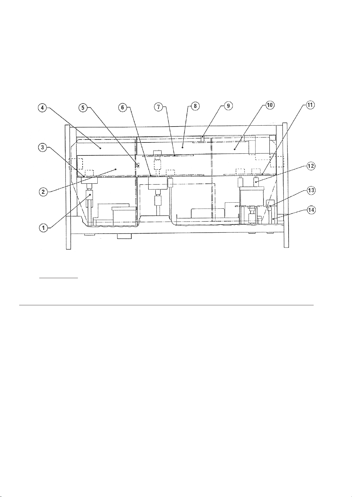
Access to the plug-in boards is obtained by removing the two screws ('A' in Fig.12 Exploded
View) and sliding back the top panel; access to the underside is by removing the two screws
('B' in Fig.12 Exploded View) and sliding back the bottom panel. The board fixing strap is
removed by undoing one screw at each end.
With certain boards it is necessary to remove the extension spindles by undoing the grub
screws in the couplers using a 6BA Allen key. Most interconnections are by plug-in connectors
but some are by soldered connections and these will
have to be unsoldered if the board or component is to be removed completely.
3.3 POWER SUPPLY VOLTAGE SELECTION (Serial No. 4515 onwards)
On models Serial No. 4515 onwards, the rear panel voltage selector mentioned in Section
2.1.1 is not fitted and adjustment to correspond to the power supply voltage is done internally.
Access is obtained by removing the two screws ('A' in Fig.12 exploded view, Appendix 4) and
sliding back the top panel. On the power supply transformer Tl (see Fig. 10), the Brown/
White lead should be unsoldered and resoldered appropriately; tag 2 - 110V, tag 3.- 220V or
tag 4 - 240V. The Blue/White lead should remain on tag 1. The rear panel must be marked
with the new voltage.
No adjustment is necessary for supply frequency in the range 50-60Hz approximately.

4. TECHNICAL DESCRIPTION / FAULTS
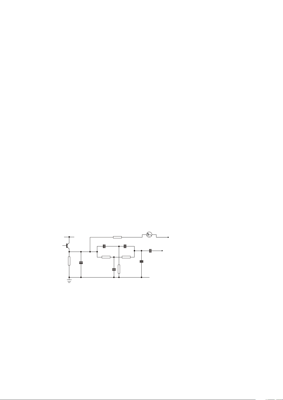
4.1. OSCILLATOR (VT1-3)
The oscillator uses three transistors in a Wien Bridge circuit, comprising two gain
stages VT1 and VT2 with an emitter follower stage VT3 to provide a low impedance
output. Negative feedback for A.C. stabilisation is provided by the potential divider
network Thermistor TH1/Resistor R7 to VT1 emitter and the D.C. conditions are
stabilised with feedback via R3/R6. The frequency of the oscillator is set by the two
parts of RV20 a& b in conjunction with C8-11 and C4-7 respectively as selected
by the Frequency Range switch SW15.
TH1
HT
+ve
R1
C8 11
R4
Fig. 1. Circuit Detail - Oscillator
FAULT
High output with excessive
distortion (squared off)
No output
R7
+
a b
RV20
VT1, 2, 3
RV19
C4 7
RV10
POSSIBLE CAUSES
Thermistor TH1 faulty-open circuit (very low
ambient temperature can cause TH1 to give
this symptom).
Transistor failure
Transistor failure
Frequency calibration wrong (all
ranges)
Frequency calibration wrong (on only
one range)
Low frequency modulation on
highest freq. range (x 1000)
Calibration of ranges wrong (not 10dB
per step)
Dial setting disturbed - reset at 14kHz. C1
faulty (open circuit)
Poor switch contact SW15. Appropriate
capacitor faulty:
x 1 C7 or C8
x10 C6 or C9
x100 CS or C10
x1000 C4 or C11
Transistor noisy. Resistor R5 noisy.
Resistor burnt out in attenuator chain-probably
R15 or R16 N.B. This is probably caused by
DC signal fed into the oscillator output socket
from the external connection-check before
reconnecting.

4.2. MILLIVOLTMETER (VT51-57)
R143
R142 &
R141
SW6a
(60dB
attenuator)
10
VT51, 52
R158
R153
SW6b
VT56, 57
+
100
+
R175
VT54, 55
SK30
Scope
Fig. 2. Circuit Detail - Millivoltmeter
The signal is fed via blocking 'capacitor C89 and overload protection resistor R144 with R143
& R142/141 providing 60dB attenuation as selected by SW6a, which thus doubles the ranges
selected by SW6b. Zener diode MR31 protects VT51 (not normally conducting) which is a field
effect transistor giving a high input impedance. The overall gain of the first stage VT51 & 52
is determined by the feedback resistor R150, which is effectively from VTS2 collector to
VT51 emitter (source), and the exact gain (approx. 10) is set by RV152 ('mV meter cal'). The
main attenuator (R153-158) has six steps (10dB per step) selected by SW6b, and these are
doubled by the 60dB attenuator SW6a to give 11 x 10dB steps and an earthed position.
Emitter follower VT53 is a unity gain buffer stage, feeding two separate amplifier stages. The
'scope' amplifier VT56 & 57 has feedback applied by R175, and the output signal is fed to the
'scope' output except when the 'W&F drift' button is pressed. The second amplifier is the main
amplifier VT54 & 55 for the meter itself, the meter being connected as part of the negative
feedback loop in a half bridge configuration as shown. R165 provides biasing for the diodes
MR32 & 33 to help the low signal linearity, and MR34 is a protection diode. C96 improves the
extreme high frequency response.
Fig. 3.
Circuit Detail-Meter
R162
VT54
R163
R164
VT55
R167
MR33
R100
C100
C98
R165
MR34
M1
R166
MR3
R169
C97
C96
The overall frequency response of the millivoltmeter circuit on the 300mV range or lower,
should be level, but on the 1V range and higher, trimmer C83 is adjusted to give a level
response (set on the 1V range). This may be done using the RTS oscillator as a source by
pressing the 'Read Osc' button. Any leads should be removed from the 'meter' and ‘osc’
sockets to avoid the effect of their capacitance.

The steep LF cut, which is 3dB down at approx. 400Hz, is applied to the circuit in three places,
the final response being as shown in Fig. 4.
(a) Normally the coupling capacitor from VT52 collector is C87 with C88 shorted. With the
'LF cut' button pressed, C87 is in series with C88 reducing the effective capacitance and
attenuating the bass frequencies.
(b) Similarly C94 is normally short-circuit but with the 'LF cut' button pressed it is in series
with coupling capacitor C93 thus reducing the capacity and hence the bass response.
(c) Normally the emitter of VT55 is decoupled by C99 in parallel with C9S. With the,'LF cut'
button pressed C99 is removed from earth and only C95 is in circuit. This reduces the
capacity and hence the bass response.
Fig. 4 L F Cut Response (Typical)
+5
0dB
-5
-10
-15
-20
-25
-30
2 3 4 5 6 7 8 9 2 3 4 5 6 7 8 9 2 3 4 5 6 7 8 9 2
100 1000 10,000
Frequency in Hz
-35

Fig. 5 DIN W & F Weighting Curve
+5
0dB
-5
-10
-15
-20
-25
-30
2 3 4 5 6 7 8 9 2 3 4 5 6 7 8 9 2 3 4 5 6 7 8 9 2
100 1000 10,000
Frequency in Hz
-35
4.3. WOW & FLUTTER (VT11-20)
The Wow & Flutter section has two distinct operations. 'Drift' gives an indication of the mean
freqency of the replay signal, disregarding short term cyclic variations. This facility is normally
used for checking the speed of an equipment against a known standard, the built-in W &F
oscillator being nominally 3150Hz (3000Hz- suffix A) within 1%. The short term drift could vary
by about 0.5% during use, after calibration in the morning following an initial warm-up period of
approx. 10 minutes.
'W & F' gives the facility of measuring peak frequency excursions of the signal around 3150Hz
or 3000Hz. All test sets will cover the range 3000-3150Hz for measuring wow and flutter
without modification, the difference between RTS and RTSA being merely a change in
frequency of the built-in W & F oscillator.
4.3.1. W & F Oscillator (VT11,12)
The transistors VT11/12 form a multivibrator whose frequency is set accurately by RV33;
'coarse' adjustment (such as converting from RTS to RTSA) can be made, if necessary, by
simultaneously changing the values of R34/35. Provision has been made to modulate the
frequency with a voltage inserted across R32 from the 'Cal' oscillator in order to set the peak
W & F calibration. The output is modified to a sinewave by filter C24/L1/C25 and fed to the
'oscillator' output when the 'W & F drift' button is pressed.
4.3.2. W & F Meter (VT13-20)
For accurate measurement a signal of at least 50mV should be fed to R39, when the high
frequencies are removed by C27 and low frequencies by C26. The residual carrier signal (at
about 3kHz) is amplified by VT13 so that it is able to drive the monostable multivibrator
VT14/15, resulting in a differentiated square wave at the collector of VT1S which is at the
frequency of the original signal. This is differentiated by C31 and rectified by MR1 (positive
half-cycle) and the emitter/base junction of VT16 (negative half-cycle). The pulse produced
bottoms VT16 once every cycle and the average current through VT16 therefore depends
linearly on the signal frequency only. The voltage developed across R46 is thus proportional to
this frequency. Transistor VT17 forms a buffer, emitter-follower stage followed by a parallel -T
filter to remove the carrier frequency, thus leaving the wow and flutter products and at the
same time the response is altered so that after the W & F components have passed C40/R60
the response has been tailored to the DIN weighting curve shown in Fig. 5 . The signals are
amplified by VT19 & 20 and fed to voltage doubler MR8 & 9, with the meter calibration
adjusted by RV69. The DC level at the collector of VT16 corresponds to the mean frequency,
and this is used for the 'drift' measurement, being compared via R52 to a fixed reference level
set by RV56 when the 'drift' button is pressed.
FAULTS
There are no specific faults to suggest; malfunctions can be traced by following the signals
through the circuit and comparing the waveforms shown on the oscilloscope with those shown
in the full circuit diagram.
Meter connection with
‘drift’ button pressed
R52
C37
R51
R53
C38
R49
VT17
C34
C36
R50
C35
Fig.6 Circuit Detail - Wow & Flutter Meter
M1
C40
To fixed reference
voltage (VT18)
To amplifier for
peak W&F measurement

4.4. DISTORTION METER (VT33-37)
In
set
100%
1
RV 111
2
Freq
1
+
10
Out
Fig. 7 Circuit Detail - Distortion Meter
The signal passes through potentiometer RV111 which sets the level into the dynamic emitter
follower stage VT33. This stage has unity gain with VT34Lacting as a constant current load for
VT33, the actual current being set by R113/R115. Bootstrapping through C64 is used to
improve the input impedance, and MR22 provides protection for VT33 in the event of overload.
VT33 is critical for noise and only low noise transistors should be used.
The base of transistor VT35 is a virtual earth point due to negative feedback via R124, which
sets the gain of the amplifier stage to approx. 10. VT35 acts as a phase-splitter with emitter
and collector loads, the ratio of their gains is approximately 2 :1 and set precisely by
potentiometers in the collector load 'phase' potentiometers. The outputs are fed to a Wien
Bridge having zero output at the selected frequency as
adjusted by the Balance phase and Frequency coarse/fine controls.
Pressing the '100%' button shorts out C64, thus removing the 'notch' in the response but
leaving the gain unaffected. With the 'read' button pressed the notch in the response is
reintroduced and C68 is shorted to earth, restricting the response to 20kHz. VT36 is an
amplification stage with an overall gain of approx. 10, VT37 giving an emitter follower output
via C69.
R120
R81
Fig. 8
Circuit Detail - Distortion
Meter (Wien Bridge)
RV121
R122
VT35
RV82 phase
C51
C66
R83
R86
R85
R88
coarse
RV84a
RV87a
RV84b
RV87b
fine
FAULT
Noise VT33 is critical for noise, and only the specified transistor should be used.
Certain components are more critical for noise - R114, R116, R117, R119,
R120, R122.
Insufficient range on Set RV121 so that meter 'nulls' when RV82 is five turns from
‘phase' control one end viz. central.
VT36

4.5. CALIBRATION (VT31,32)
The 'Call oscillator is mounted on the Distortion Meter Board and consists of a multivibrator
operating at approx. 70Hz. A 'square wave' output is taken from each collector, that from VT31
collector being used to modulate the W & F oscillator with calibration set by RV101. The output
from VT32 is stabilised further by zener diode MR21 and further reduced to give an indication
of 0dBm on 1V range of the millivoltmeter set by RV110 as a calibration standard.
The cal oscillator is only operational when the 'cal' button is pressed.
Fig. 9 Distortion Filter Response (Typical)
+1
2 3 4 5 6 7 8 9 2 3 4 5 6 7 8 9 2 3 4 5 6 7 8 9 2
100 1000 10,000
Frequency in Hz
0dB
-1
-2
-3
-4
-5
-6
-7

5. CALIBRATION
In the setting up of the RTS, it is necessary to use test instruments of sufficient accuracy to
calibrate each section to the required performance. In general these should be of the order of
ten times more accurate than the RTS, particularly the Millivoltmeter. In an emergency, less
accurate test equipment may have to be used, but the accuracy of the RTS will then not
necessarily conform exactly to specification and this must be borne in mind when making
measurements.
5.1.Test Equipment Required
(a) Millivoltmeter MV
(b) Digital Frequency Meter DFM
(c) Distortion Meter DM
(d) Oscilltor (sine wave) 0
(e) Oscilloscope S
(f) Function Generator & LF Oscillator
(see Wow & Flutter 5.6.3)
5.2. Power Supply
(a) Using the Millivoltmeter MV, check that the voltage on the pin (red lead) of the Power
Supply Board is 30V dc relative to chassis; if necessary reset RV192 on the Power
Supply Board (Fig.10 )
5.3. Oscillator
(a) Set the Oscillator output controls, Coarse & Fine, to maximum (fully clockwise) and set
the dial and push button controls to give an output of 14kHz at the Oscillator output
checked by the Frequency Meter DFM.
(b) Check that the dial indicates 14kHz; if necessary reset this by slackening the grub
screw and rotating the dial to 14kHz before retightening (on later models remove the
knob cover/insert, slacken the collet nut then retighten with the dial at 14kHz).
(c) Check that with the dial set to 4kHz the Frequency Meter DFM reading is within t 5%
(3.8 to 4.2kHz).
(d) Check the frequency accuracy similarly on the other ranges.
Dial
4 kHz
40 Hz
400 Hz
40 kHz
Frequency Limits
3.8 kHz to 4.2 kHz
38 Hz to42 Hz
380 Hz to 420 Hz
38 kHz to 42 kHz

(e) Using the Millivoltmeter MV, check that the output from the oscillator with the coarse &
fine controls at maximum is greater than 2.8V (at 1kHz approx.)
(f) Check that the 'Output' control 'Coarse' operates in steps of 10dB t 0.5dB.
(g) At 0dB on the 1V range of the Millivoltmeter MV, check that the frequency response is
level at 1kHz, 15 Hz , 40Hz, 15kHz, 150kHz, within ±0.2dB
(h) Set the oscillator output to 1V at 1kHz and using the Distortion Meter DM check that the
distortion is less than .025%.
5.4. Millivoltmeter
(a) With nothing connected to the 'meter' socket and the milli-voltmeter set to the 30V
range, check that the meter reads zero; if necessary reset the meter to zero using the
adjustment at its rear.
(b) Feed the Oscillator 0 into both the RTS and the Millivolt-meter MV, setting each to the
1V range.
(c) Set the Oscillator 0 to lkHz and adjust its output to give a reading of 0.8V on the
Millivoltmeter MV.
(d) Check that the RTS millivoltmeter also reads 0.8V; if necessary adjust the preset control
'mV meter cal' RV152 on the front panel.
(e) Check that the frequency response agrees with the Milli-voltmeter MV over the ranges
1kHz to 20kHz within ± 1% and over 15Hz to 150kHz within ± 2%; if necessary adjust
trimmer capacitor C83 to give as level a high frequency response as possible.
(f) Recheck the reading of 0.8V (at 1kHz) on both meters; if necessary reset RV152.
(g) Press 'calibrate' and check that the RTS millivoltmeter reads 0dB (still on 1V range); if
necessary reset RV110 on the Distortion Meter Board (then press 'calibrate' to release).
(h) With the Oscillator 0 set to 400Hz, press 'LF cut' and check that the response is reduced
by 3dB (± 1dB).
(i) Reset the Oscillator 0 to 1kHz and adjust the output to give a meter reading of 0dB (on
1V); switching the input signal level in 10dB steps, check that on all ranges the RTS
millivoltmeter agrees with the Millivoltmeter MV within ± 2% (one division of the top
scale).
5.5. Distortion Meter
(a) It is not essential but nevertheless highly desirable that the Oscilloscope S be
connected to the 'scope' socket throughout this section, thus enabling the output to be
observed to ensure that it is signal rather than noise.

(b) Set the 'balance' controls to their centre positions ('Phase' control 5 complete turns from
one end).
(c) With the Oscillator 0 still set to 1kHz, press 'set 100V and adjust the 'Sensitivity' control
to give full scale reading on the 1V range.
(d) Press 'read' &'LF cut' and adjust the pre-set phase control RV121 on the Distortion
Meter Board together with the 'freq coarse' & 'fine' controls on the front panel alternately
to give minimum reading, reducing the milli-voltmeter range as required.
(e) If necessary, the final reading can be obtained using the 'phase' control on the front
panel, but this must not be more than two full turns from its centre position.
(f) The final reading should be less than 0.025% (assuming that the inherent distortion of
the Oscillator 0 is much less than this).
Note: Modification of RTS2 Distortion Measurement Frequency
The frequency range of the RTS2 distortion measurement can be modified to operate at a
different frequency instead of the normal 400-1100Hz approximately by altering the value of
C51 & C66 simultaneously. In practice the value of these capacitors is not critical, but they
must have the same value within 1%. A suggested table of values is given below; values to
give other frequency ranges can be determined by proportion.
C51& C66
0.33mF
0.22mF
0.1mF
.056mF
.033mF
.022mF
.01mF
5600 pF
3300 pF
*Because of the low frequency of operation after this modification has been carried out, the 'LF
cut' button must not be pressed while making distortion measurements. The residual reading
obtainable will therefore depend upon the level of hum, etc., in the signal and this will
determine the minimum percentage distortion which can be read, although this will normally be
adequate for most 'off tape' measurements.
Freq.Range
approx.
40 - 110 Hz*
60 - 165 Hz*
132- 360 Hz*
235- 650 Hz*
400 -1100 Hz
600 -1650 Hz
1.32- 3.6 kHz
2.35- 6.5 kHz
4 - 11 kHz

5.6. Wow & Flutter Meter
5.6.1. Oscillator
(a) Connect the Digital Frequency Meter DFM to the 'oscillator' output, press 'W & F drift'
and check the frequency of the W & F oscillator; if necessary adjust RV33 on the W & F
Board to set the frequency to 3150Hz (or 3000Hz) ± 1%.
Note: If RV33 does not give enough adjustment, alter the values of R34/R35 simultaneously
to bring the frequency within range (about 5-10% each should be sufficient), increasing
the value to reduce the frequency and vice versa.
(b) Connect the Millivoltmeter MV to the 'oscillator' output and check that the output is
350mV or greater ; if necessary tune Ll on the W & F Board for maximum output.
5.6.2. Drift
(a) Connect the Oscillator 0 and Digital Frequency Meter DFM in parallel across the 'meter'
input and set the Oscillator 0 accurately to 3150Hz (or 3000Hz).
(b) Press 'W & F drift' and 'drift', and adjust the 'drift set zero' control RV56 to give zero drift
on the meter (centre scale).
(c) Set the Oscillator 0 to ± 1% (3181.5Hz or 3030Hz) then to -1% (3118.5Hz or 2970Hz),
and check that the meter reads accordingly; if necessary adjust the drift sensitivity
potentiometer RV54 on the W& F Board to indicate ± 1% on the RTS meter scale.
(d) If RV44 has been adjusted, recalibrate zero drift as in (b) above and repeat (c); the
settings of RV54 & RV56 are interdependent and (b) & (c) must be repeated alternately
until no further adjustment is necessary.
(e) Remove the connections to the 'meter' socket on the RTS and press 'calibrate' (in
addition to 'W & F drift').
(f) Check that the meter reads zero (centre scale); if necessary adjust 'drift set zero' pre-
set control.
5.6.3. Wow & Flutter
(a) Connect to the RTS 'meter'• input a sine wave of 3150Hz (or 3000Hz) frequency
modulated to 0.3% peak by a 4Hz sine wave; this can be obtained from a function
generator and low frequency oscillator or another function generator.
(b) Press '0.3%' and check that the meter reads 0.3%; if necessary adjust the pre-set
control 'peak wow-cal (0.3% range)' RV69.
(c) If available, connect the Oscilloscope S to the 'scope' socket and check that a
sinusoidal wave form is shown.
(d) Press 'calibrate' and check that the meter reads on the 'cal' mark; if necessary, adjust
the cal control RV101 (lower left) on the Distortion Meter Board.

T1
0V
110V
1 2 3 4
5 6 7
220V
240V
Fig. 10 Component location - General
R196
VT
R193
inP k
+
C122
72
Green
+
C123
MR
VT71
RV
192
C121
V o et
VT
52
-
{
73
Wh te
Pink
-
MR51+
R191
R195
POWER BOARD
R194
Red
Neutra Bra d
B ue Red
B ue
SKT10
R212
R211
SKT20
WOW & FLUTTER BOARD
1 13
M1
Meter
+ -
SKT11
WOW & FLUTTER
dr ft 1% 0.3% 0.1%
WOW & FLUTTER MOTHER BOARD
Ca
meter
socket
SK31
Osc ator
socket
SK32
Scope
socket
SK30
POTENTIOMETER
MOUNTING
BOARD
SW10
C51
RV87
R83
R85
R88
R86
Neutra
R81
B ue
Red
RV82
RV84
Bra d
1 DISTORTION METER BOARD 13
1 MILLIVOLTMETER BOARD 13
SKT1
1 OSCILLATOR BOARD 13
Orange
B ue
{
MILLIVOLTMETER W&F DISTORTION
LF cut Osc Input Dr ft 100% Read Ca
X1 X10 X100 X1000
FREQUENCY
Orange
MILLIVOLTMETER MOTHER BOARD
OSCILLATOR MOTHER BOARD
Osc.
Freq.

C43 MOUNT ON
COPPER SIDE ACROSS R40
MR8
MR9
MR3
C12
RV34
R67
R68
+C43
R52
R64
R66
VT18
C44+
R61
R55
R59
R42
C28
R40
C27
R63
VT20
R55
R38
C26
RV69
R70
R60
MR4
C29
VT14
VT13
VT19
MR5
R41
R39
R62
VT11
C22
C24
R37
R58
C40
+ C41 -
C30
R44
VT15
C21
C23
C38
MR16
VT12
RV56
C35
MR17
MR1
R43
R53
R51
R45
R34
R31
R35
R36
R53
R49
C34
C33
VT
16
R57
MR
2
C39 +
R32
R50
C36C37
R48C31
R47
C32
RV33
L1
VT17
R46
R122
C66
R124
R129
C68
VT33
R119
R126
+ C67
VT36
C69
R117
VT35
R127
RV121
R53
VT37
R128
RV 111
R120
R116
R112
+ C64
R114
R113
C65
R123
RV101
+ C63
MR
22
R102
R108
VT34
R104
R103
C61
R105
R106
R107
R109
R118
R115
VT31
C62
VT32
MR21
RV110
Fig. 11a Wow & Flutter Board
025 312
R158
R53
C
83
C91
C88 C82
R160
MR35
VT53
R172
R161
R175
R171
R174
VT57
C101
SW4
C92
R178
VT
56
R173
R156R157
C90
R153
C93+
R155
R154
14
3
R142 R141
C87 +
R166
R162
VT
54
R
C95
R167
R164
C99 +
R163
C102 +
RV132
C94
VT51
R147
R146
+C86
R53
VT
55
R151
R165
R145
MR
31
R150
MR
32
MR
33
C97 +
C98 +
+C100
C103 +
C96 R169 R176
+ C85
R149
R148
R168
R144
VT52
MR
34
C89
Fig. 11b Distortion Meter Board
025 320
C81
R15R14
SW1
R13
R11
R17
R12
R16
R8
R5
R3
R7
C2 +
+ C3
TH1
RV19
R10
R9
C7
C5
C4
C6
R6
R1
R4
VT1
C8
C9
C10
C1
UNDER
VT3
VT2
C2
R18
C11
Fig. 11c Millivoltmeter Board
025 322
Fig. 11d Oscillator Board
025 245
Fig. 11 Component Location

Comments
After
Serial No. 3200+
Item 9, Appdx. 1 Front view
Type 16 (coupling 202-005)
Side panel 320-047
025-255 (Fixing modified)
Control knob 448-080
See 6.2 & Appendix 1a
See 589 above
Items 9 & 10 of Front view
Appendix 1 are 022-468
Serial No. 4515+
See 6.2
Item 1, Appendix 4
Handles, rear panel-light grey
Changed to suit potentiometers
Knob 448-087
Cap 448-088
Insert 440-038
Rear panel 573-177 Issue 3
(Mains supply plug added)
Rear panel 573-177 Issue 4
(VT73 transistor BD535)
Front extrusion 573-179
(printing deleted)
6. HISTORY OF MODIFICATIONS
RV56,69,152-type 44(202-003)
Before
Change
Date
6.1 Mechanical
Side panel 320-036
Millivoltmeter mother board
Control knob 448-025
Handles, rear panel-dark grey
Extension spindles, couplers
Control knob 448-080
(no longer manufactured)
Rear panel 573-177 Issue 2
(Voltage selector deleted)
Rear panel 573-177 Issue 3
(VT73 transistor 40312)
Front extrusion 573-180
No
279
299
582
589
591
666
679
Jan.73
Jul.76
Apr.73
Feb.78
Mar.78
692
May 78
702
716
Jul.78
Sep.78

Comments
Add to copper side
of board.
After
Before
Cct.
Ref.
560R 0.5W 5% 625-12-560
390k 1% 625-24-390k
39k 0.5W 5% 625-12-39k
56k 0.5W 5% 625-12-56k
22R 0.5W 5% 625-12-22
12.5mF 25V Electrolytic 130-026
Zener Diode BZY88C12 290-017
0.047mF 131-256
47K 0.25W 5% 625-12-47K
1000pF 63V 2.5% 131-768
470R 0.5W 10% 625-13-470
360K 1% 625-24-360k
33k 0.5W 10% 625-13-33k
47k 5% 624-001
Not fitted
25mF 25V Electrolytic 130-016
.022mF 131-255
56k 0.5W 5% 625-13-56k
950pF 63V 21% 131-775
R43
R47
R48
R5
R141
C43,4
C32
R40
MR 2
C21,22
950pF 63V 2.5% 131-775
1.8k 1% 625-24-1k8
1.6k 1% 625-24-1k6
180R 0.25W 5% 625-07-180
Type 16 + coupling 202-005
(spindle 4mm)
(fixing hole 7mm)
0.1mF 100V 2% 131-514
1mF 100V 2% 131-515
950pF 63V 21% 131-775
Not fitted
2.2k 1% 625-24-2k2
1.8k 1% 625-24-1k8
180R 0.5W 5% 625-12-180
Type 44 + coupling 202-003
(spindle 0.125 in)
(fixing hole 0.25 in)
0.1mF 1%
1mF1%
1000pF 64V 21% 131-768
R176
R4
RV56
RV69
C45
R1
RV152
C6,9
C7,8
C21,22
396
179
Change
No.
Date
6.2 Electrical
136
RTS 1
May 71
142
May 71
May 71
239
RTS 2 (Serial No. 730+)
Aug.72
Oct.72
Jan.73
Jan.73
279
275
251
370
Oct.73
Nov73

Comments
No change necessary
unless 'scope probe used
prior to Serial No. 2700
Should be fitted to
earlier models to
avoid switching surges
Later version fits
all models.
Fit later assembly
022-XXX as replacement
for earlier pot.
See Section 3.3
Serial No.4515+
After
1k 0.25W 0.2% 624-033
1M 0.25W 0.2% 624-032
Diode BAX16 290-001
or MAX16, or 1N4148
(pole SW6b earth)
582-033 (spindle reduced
by 0.25in)
582-109 + 705-028B = 022-528
582-107 + 705-028G = 022-527
582-108 + 705-028E = 022-526
10k 625-28-10k
Ti Transformer tags
Plug, power supply 577-017
Socket & lead 578-018
Label 450-171
“ 110V 50/60Hz 450-172
“ 220V 50/60Hz 450-173
“ 240V 50/60Hz 450-174
Transistor BD535 825-074
Fuse 1A 380-000
Fuse holder Bulgin 380-017
or (Schurter) 1380-017
Before
R142 2k 0.25W 0.2% 624-016
R143 1M 0.25W 0.2% 624-017
Cct.
Ref.
R142
R143
510
Change
No.
6.2 Electrical
Date
May 75
Not fitted
576
June 76
582-033
582-034
582-035
582-036
47k 625-28-47k
Voltage selector
(no longer manufactured)
Not fitted
VS1
RV87
666
589
July 76
May 78
R8
RV19
RV111
692
670
Jan 78
May 78
P1
VT73 Transistor 40312 825-002
Fuse 0.75A 380-008
Fuseholder 380-005
FS1
VT73
702
July 78

FERROGRAPH
RECORDER TEST SET
FRONT VIEW RTS 2
Appendix
Ref. RTS2
Number Item Qty. Part No.
1 Socket 3 692-030
2 Button 15 448-019
3 Knob K2 2 448-021
4 Bush 4 100-037
5 Extension Spindle 1 705-028F
6 Knob K2W 2 448-023
7 Extension Spindle 1 705-028D
8 Zero Stud 1 666-071
9 Knob K3 1 448-080
10 Dial 1 295-004
11 Potentiometer 10k Logarithmic 1 582-033
12 Extension Spindle 1 705-028C
13 Extension Spindle 1 705-028E
14 Meter 1 512-005
15 Lamp Holder 1 455-008
16 Lamp Festoon 3W 1 455-010(12V)
17 Knob K1 2 448-022
18 Extension Spindle 2 705-028A
19 Knob K 1W 2 448-026
20 Bush 3 100-038
21 Extension Spindle 3 705-029
22 Front Panel 1 573-178

FERROGRAPH
RECORDER TEST SET
REAR VIEW
Ref. RTS 2
Number Item Qty. Part No.
1 Mains Transformer 1 T1721
2 Fuse Holder 1 380-005
3 Fuse (0.75A, 20mm x 5mm dia.) 1 380-008
4 Vol tage Sel ector 1 920-001
5 Grommet 1 398-014
6 Power Board 1 025-310
7 Transistor (type 40312) 1 825-002
8 P.C. Board Support Bracket 1 025-255
9 Power Supply Lead 1 110-017
10 Cable Clip 2 196-011
11 Spacer 4 698-079
FERROGRAPH
RECORDER TEST SET
PLAN VIEW
Ref. RTS 2
Number Item Qty. Part No.
1 Coupling 6 687-029
2 P. C. Board Fixing Strap 1 025-256
3 Oscillator Board 1 025-245
4 Oscillator Mother Board 1 025-247
5 Terminal Nut 4BA 1 BP/2025/N
6 Millivoltmeter Board 1 025-322
7 Distortion Meter Board 1 025-320
8 Millivoltmeter Mother Board 1 025-248
9 Spacer 9 698-068
10 Wow & Flutter Mother Board 1 025-311
11 Wow & Flutter Board 1 025-312
12 Coupling 3 202-005
13 Potentiometer Mounting Board 1 025-309
14 Spacer 4 698-069

FERROGRAPH
RECORDER TEST SET
EXPLODED VIEW RTS2
Ref. RTS2
Number Item Qty. Part No.
1 Front Extrusion 1 573-180
2 Handle 2 412-002
3 Side Panel Extrusion 2 320-036
4 Hoop Frame 2 360-003
5 Bracket (top strap, L. H. ) 1 025-254A
6 Screen 1 671-005
7 Rear Panel 1 573-177
8 Top Panel 1 573-143
9 Bottom Panel 1 573-144
10 Bracket (top strap, R. H.) 1 025-254B

FERROGRAPH
RECORDER TEST SET
List of Components
Cct. Cct.
Ref. OSCILLATOR BOARD Part No. Ref. WOW & FLUTTER BOARD Part No.
R1 1.8k 1/4W 1 % High Stab. 625 24 1k8 R31 3.3k 1/2WW 5% 625 12 3k3
Resistors (R) & Potentiometers (RV) Resistors (R) & Potentiometers (RV)
R2 15k 1/2W 10% 625 13 15k R32 1k0 1% High Stab. 625 24 1k
R3 10k 1/2W 5% 625 12 10k RV33 22k Linear SET 3150Hz 582 012
R4 1.6k 1/4W 1% High Stab. 625 24 1k6 R34 430k 0.25W 2% High Stab. 625 25 430k
R5 560R 1/2W 5% 625 12 560
R6 47k 1/2W 10% 625 13 47k R35 430k 0.25W 2% High Stab. 625 25 430k
R7 820R 1/2W 5% 625 12 820 R36 3k3 0.5W 5% 625 12 3k3
R8 47k 1/2W 10% 625 13 47k R37 5.6k 0.5W 5% 625 12 5k6
R9 1k 1/4W 1% High Stab. 625 24 1k R38 10M 0.5W 10% 625 13 10M
R10 620R 1/2W 5% 625 12 620 R39 22k0 0.5W 10% 625 13 22k
R11 1370R 1/4W 0.2% High Stab. 624 015
R12 432R 1/4W 0.2% High Stab. 624 014 R40 47k 0.25W 5% High Stab 624 001
R13 137R 1/4W 0.2 % High Stab. 624 013 R41 22k 0.5W 10% 625 13 22k
R14 43.2R 1/4W 0.2% High Stab. 624 012 R42 3.3k 0.5W 5% 625 12 3k3
R15 13.7R 1/4W 0.2% High Stab. 624 011 R43 390k 0.25W 1% High Stab 625 24 390k
R16 6.34R 1/4W 0.2% High Stab. 624 010 R44 22k 0.5W 10% 625 I3 22k
R17 100R 1/2W 5% 625 12 100
R18 100R 1/2W 5% 625 12 100 R45 3.3k 0.5W 5% 625 12 3k3
RV19 2.2k0 Linear (OUTPUT fine) 582 035 R46 22k 0.25W 1% High Stab 625 24 22k
Cl 3300mF 40V Electrolytic 130 024
C2 125mF 16V Electrolytic 130 002
C3 125mF 16V Electrolytic 130 002
C4 950pF 30V 2 1/2% 131 775
C5 0.01mF 30V 2 1/2 % 131 774
C6 0.1mF 160V 2 1/2% 131 514
C7 1mF 160V 2 1/2% 131 515
CO 1mF 160V 2 1/2% 131 515
C9 0.1mF 160V 2 1/2% 131 514
CIO 0.01mF 30V 2 1/2% 131 774
C11 950pF 30V 2 1/2 % 131 775
VT1 Transistor BC183LB 825 015
VT2 Transistor BC154LB 825 016
VT3 Transistor BC183LB 825 015
SW1 Switch (OSC. OUTPUT coarse) 750 013
TH1 Thermistor ITT R25 800 000
Cct.
Ref. Front Panel Part No
RV20a 10k0 Log. (FREQ.) 582 033
RV20b 10k Log
MI Meter (Sifam 100mA) 512 005
LP1 Lamp 12V, 3W 455 010
SKT30 Socket BNC (1637/CS) 692 030
SKT31 Socket BNC (1637/CS) 692 030
SKT32 Socket BNC (1637/CS) 692 030
Capacitors
Miscellaneous
Miscellaneous
R47 39k 0.5W 5% 625 12 39k
R48 56k 0.5W 10% 625 13 56k
R49 22k 0.5W 10% 625 13 22k
R50 1k0 0.5W 10% 625 13 1k
R51 620R 0.5W 5% 625 12 620
R52 2.2k 0.25W 1% High Stab. 625 24 2k2
R53 1k 0.5W 10% 625 13 1k
RV54 1k Linear DRIFT SENS. 582 032
R55 22k 0.5W 10% 625 13 22k
RV56 25k Linear drift set zero 582 055
R57 22k 0.25W 1% High Stab. 625 24 22k
R58 33k 0.25W 1% High Stab. 625 24 33k
R59 33k 0.25W 1% High Stab. 625 24 33k
R60 100k 0.25W 5% High Stab. 624 002
R61 220k 0.5W 5% 625 12 220k
R62 1.6k 0.25W 1% High Stab. 625 24 11,6
R63 1M 0.5W 10% 625 13 1M
R64 4.7k 0.5W 5% 625 12 4k7
R65 390R 0.24W 1% High Stab. 625 24 390
R66 100k 0.25W 5% High Stab, 624 002
R67 1.6k 0.25W 1% High Stab. 625 24 1k6
R68 56k 0.5W 5% 625 12 56k
RV69 25k Linear peak wow cal. 582 055
R70 470R 0.5W 10% 625 13 470
C21 950pF 63V 2i% 131 775
C22 950pF 63V 2% 131 775
C23 0.22µF 100V 10% 131 253
C24 0.220F 100V 10% 131 253
C25 O. 33pF 100V 10% 131 257
C26 950pF 63V 2 % 131 775
C27 950pF 63V 2 % 131 775
C28 950pF 63V 2 % 131 775
C29 950pF 63V 2 % 131 775
Capacitors

FERROGRAPH
RECORDER TEST SET
List of Components
Cct. Cct.
Ref. WOW & FLUTTER BOARD Part No. Ref. POT. MOUNTING BOARD Part No.
C30 950pF 63V 2% 131 775 Capacitors
C31 0.01pF 30V 2 % 131 774 C51 0.033uF 250V 1% 131 260
C32 0.0470F 250V 10% 131 256
C33 0.22µF 100V 10% 131 253 Miscellaneous
C34 0.22pF 100V 10% 131 253 SW10 Switch SUPPLY on 750 004
C35 0.1pF 100V 10% 131 250
C36 0.047µF 250V 10% 131 256 DISTORTION METER BOARD
C37 0.047pF 250V 10% 131 256
C38 0.047µF 250V 10% 131 256 Resistors (R) & Potentiometers (RV)
C39 25uF 25V Electrolytic 130 016 RV101 22k Linear SET W&F CAL 582 012
C40 1uF 250V 10% 131 259 R103 47k 0.25W 5% High Stab. 624 001
C41 25uF 25V Electrolytic 130 016 R104 360k 0.25W 1% High Stab. 625 24 360k
C42 0.22µF 100y 10% 131 253
C43 12.5uF 25V Electrolytic 130 026 R105 360k 0.25W 1% High Stab. 625 24 360k
C44 12.5uF 25V Electrolytic 130 026 R106 18k 0.5W 10% 625 13 18k
C45 950pF 63V 21% 131 775 R107 4.7k 0.25W 1% High Stab. 625 24 4k7
VT11 Transistor BC184LC 825 005
VT12 Transistor BC184LC 825 005 RV110 22k Linear SET mVmeter CAL 582 012
VT13 Transistor BC184LC 825 005 RV111 100k Log. set 100% 582 036
VT14 Transistor BC 183LB 825 015 RI12 1k 0.5W 10% 625 13 1k
VT15 Transistor BC183LB 825 015 R114 33k 0.25W 1% High Stab. 625 24 33k
VT16 Transistor BC183LB 825 015
VT17 Transistor BC184LC 825 005 R115 1.8k 0.5W 10% 625 12 1k8
VT18 Transistor BC184LC 825 005 R116 22k 0.25W 1% High Stab. 625 24 22k
VT19 Transistor BC184LC 825 005 R117 47k 0.25W 1% High Stab. 624 001
VT20 Transistor BC183LB 825 015 R119 3.3k 0.5W 5% 625 12 3k3
MR1 Diode MAX16 290 001 R120 1.8k 0.25W 1% High Stab. 625 24 1k8
MR2 Zener Diode BZY88C12 290 017 RV121 1k Linear SET PHASE BAL. 582 032
MR3 Diode NKT249A30 290 015 R122 1k 0.25W 1% High Stab. 625 24 1k
MR4 Zener Diode BZY88C5V6 290 013 R123 1.8k 0.5W 5% 625 12 1k8
MR5 Zener Diode BZY88C4V7 290 016
MR6 Zener Diode BZY88C4V7 290 016 R125 100k 0.25W 5% High Stab. 624 002
MR7 Zener Diode BZY88C4V7 290 016 R126 270R 0.5W 5% 625 12 270
MR8 Diode NKT 249A30 290 015 R127 47k 0.25W 5% High Stab. 624 001
MR9 Diode NKT 249A30 290 015 R128 10k 0.5W 10% 625 13 10k
L1 Coil Spec 800
POT. MOUNTING BOARD C62 0.1uF 100V 10% 131 250
Resistors (R) Er Potentiometers (RV) C63 640uF 25V Electrolytic 130 004
R81 10k 0.25W 1% High Stab. 625 24 10k
RV82 2k 10 turn BALANCE phase 582 056 C65 0.47uF 250V 10% 131 258
R83 3.9k 0.5W 5% 625 12 3k9 C66 0.033uF 250V 10% 131 262
RV84a 10k Log. (Freq. coarse) 582 094 C67 25uF 25V Electrolytic 130 016
RV84b 10k Log. C68 4700pF 30V 21/2% 131 778
R85 3.9k 0.5W 5% 625 12 3k9
R86 330k 0.5W 5% 625 12 330k
RV87a 100k Log. (Freq. fine) 582 034
RV87b 100k Log.
R88 330k 0.5W 5% 625 12 330k
Capacitors
R102 47k 0.25W 5% High Stab. 624 001
Miscellaneous R109 6k8 0.25W 1% High Stab. 625 24 6k8
R108 10k 0.25W 1% High Stab. 625 24 10k
R113 22k 0.25W 1% High Stab. 625 24 22k
R118 100R 0.5W 5% 625 12 100
R124 39k 0.5W 10% 625 13 39k
R129 1.5k 0.5W 5% 625 12 1k5
C61 0.1uF 100V 10% 131 250
C64 25uF 25V Electrolytic 130 016
C69 0.47uF 250V 10% 1310258
Capacitors

FERROGRAPH
RECORDER TEST SET
List of Components
Cct. Cct.
Ref. DISTORTION METER BOARD Part No. Ref. MILLIVOLTMETER BOARD Part No.
VT31 Transistor BC183LB 825 015
VT32 Transistor BC183LB 825 015 R175 10k 0.5W 5% 625 12 10k
VT33 Transistor 2 SC 1000BL 825 035 R176 180R 0.5W 5% 625 07 180
VT34 Transistor BC183LB 825 015
VT35 Transistor 2 SC 1000 BL 825 035 Capacitors
VT36 Transistor 2 SC 1000 BL 825 035
VT37 Transistor 2 SC 1000 BL 825 035 C81 500pF 160V 10% 131 765
MR21 Zener Diode BZY88C5V6 290 013 C82 0.01µF 30V 2.5% 131 774
MR22 Diode MAX 16 290 001 C83 Variable Ceramic 131 001
Cct. C86 5uF 64V Electrolytic 130 007
Ref. MILLIVOLTMETER BOARD Part No. C87 32uF 40V Electrolytic 130 013
R141 22R 0.5W 5% 625 12 22 C89 0.1µF 400V 10% 131 516
R142 2K 0.5W 0.2% High Stab 624 16
R143 2M 0.5W 0.2% High Stab 624 17 C90 0.022uF 250V 10% 131 255
R144 1K 0.5W 5% 625 12 1K C91 0.22uF 100V 10% 131 253
R145 180R 0.5W 1% High Stab 625 24 180 C93 5uF 64V Electrolytic 130 007
R146 1K 0.5W 5% 625 12 1K C94 0.047uF 250V 10% 131 256
R147 10K 0.5W 5% 625 12 10K
R148 1K 0.5W 1% High Stab 625 24 1K C95 0.1uF 100V 10% 131 250
R149 270K 0.5W 5% 625 12 270K C96 500pF 160V 10% 131 765
R150 1.5K 0.5W 1% High Stab 625 24 1.5K C98 25uF 25V Electrolytic 130 016
R151 470R 0.5W 5% 625 13 470 C99 25uF 25V Electrolytic 130 016
RV152 2K Linear MVmeter Cal. 528 054 C100 12.5uF 25V Electrolytic 130 026
R153 6.34R 0.5W 0.2% High Stab 624 010 C101 0.22uF 100V 10% 131 253
R154 33.7R 0.5W 0.2% High Stab 624 011 C102 125uF 16V Electrolytic 130 002
R155 43.2R 0.5W 0.2% High Stab 624 012
R156 137R 0.5W 0.2% High Stab 624 013 Miscellaneous
R157 432R 0.5W 0.2% High Stab 624 014 VT51 Transistor 2SK30GR 825 006
R158 1370R 0.5W 0.2% High Stab 624 015 VT52 Transistor BC 184LC 825 005
R159 470R 0.5W 0.2% High Stab 625 13 470 VT53 Transistor BC183LB 825 015
R160 10M 0.5W 10% 625 13 10M VT55 Transistor BC183LB 825 015
R161 100K 0.5W 5% High Stab 624 002 VT56 Transistor BC183LB 825 015
R162 100K 0.5W 5% High Stab 624 002 VT57 Transistor BC183LB 825 015
R163 47R 0.5W 1% High Stab 625 24 47
R164 470K 0.5W 10% 625 13 470K MR31 Zener Diode BZY88C5V6 290 013
R165 620R 0.5W 5% 625 12 620 MR33 Diode MAX16 290 001
R166 10K 0.5W 5% 625 12 10K MR34 Diode MAX16 290 001
R167 1.5K 0.5W 10% 625 13 1.5K MR35 Zener Diode BZX70C20 290 011
R168 1K 0.5W 1% High Stab 625 24 1K (or 3TZ20 or 1N5357B)
R169 1K 0.5W 1% High Stab 625 24 1K
R170 100R 0.5W 5% 625 12 100
R171 220K 0.5W 10% 625 13 220K
R172 470K 0.5W 10% 625 13 470K POWER BOARD
R173 1K 0.5W 5% 625 12 1K Resistors (R) & Potentiometers (RV)
R174 15K 0.5W 5% 625 12 15K R191 22k 0.5W 1% High Stab. 625 24 22k
Miscellaneous Resistors (R) & Potentiometers (RV)
C84 160uF 25V Electrolytic 130 011
C85 125uF 16V Electrolytic 130 002
C88 0.22uF 100V 10% 131 253
C92 0.22uF 100V 10% 131 253
C97 25uF 25V Electrolytic 130 016
C103 160uF 25V Electrolytic 130 011
VT54 Transistor BC183LB 825 015
MR32 Diode MAX16 290 001
SW6 Switch M1LLIVOLTMETER 750 014
RV192 1k0 Linear SET 30V D.C. 582 032
R193 4.3k 0.5W 1% High Stab. 625 24 4k3
R194 3.9K 0.5W 5% 625 12 3k9
R195 100k 0.5W 10% 625 13 100k
R196 10k 0.5W 10% 625 13 10k

FERROGRAPH
RECORDER TEST SET
List of Components
Cct.
Ref. POWER BOARD Part No. Cct.
C121 100uF 40V Electrolytic 130 001 R212 137R 0.5W 0.2% High Stab. 624 013
0122 0.01uF 100V 10% 131 500
C123 250uF 64V Electrolytic 130 010 SW25 Push Button Switch W & F 749 005
VT71 Transistor BC183LB 825 015
VT72 Transistor BC461 825 032 OSCILLATOR MOTHER BOARD
MR51 Zener Diode BZY88C5V6 290 013 SKT1 P.C. Board Socket 26 way 692 029
MR52 Bridge Rectifier W02 600 002
VT73 Transistor 40312 825 002 SKT10 P.C. Board Socket 26 way 692 029
T1 Transformer, Power Supply T1721
FS1 Fuse 0.75A, 20mm x 5mm dia. 380 008
VS Voltage Selector 920 001
Capacitors R211 680R 0.5W 1% High Stab. 625 24 680
Miscellaneous
REAR PANEL. SW20 Push Button Switch 749 003
Ref. W F MOTHER BOARD Part No.
SKT20 P. C. Board Socket 26 way 692 029
SW15 Push Button Switch FREQUENCY 749 005
MILLIVOLTMETER MOTHER BD
SKT11 P.C. Board Socket 26 way 692 029
REPLACEMENT BOARD SERVICE
Where it is found necessary to change an electronic component, the RTS2
should be checked and re-calibrated using test equipment which is several
times more accurate than the Test Set itself. If this equipment is not
available or if difficulty is experienced, the relevant P.C. board(s) can be
sent for checking or replacement to the Ferrograph !Replacement Board
Service!.
When returning the board(s) to the appropriate overseas agent, or in the
U.K. to theU. K. SERVICE DEPARTMENT . It is essential to include the
SERIAL NUMBER of the Test Set.

SKT1
+30V
R18
SW1
OSC
O/P
COARSE
20V
R31
10V
C21
POLE CONTACT RELATIONSHIP
R32
RV33
SET
3150Hz
R35R34
7.7V
C22
VT11
VT12
SWITCH INDEX SHOWING
POLE
DEPRESSED RELEASED
R36
C23
C24
CONTACT
R37
16V
C25
R47
C32
VT16
12V 3V
VT17
R48
C34
C33
R49
C35
drift
DRIFT
SENS
R55
SKT 20
set zero
RV56
VT8
7.5 - 9.4
(RV56)
20V
C39
MR4
8V
R50
R52
C36
R51
1 2 3 4 5 6 7 8 9 10 1112 13
+30V
MR3
R53
C37
C38
MR5
MR6
MR7
RV54
C40
R57
R58
R59
R211
R70
R60
C41
VT19
R61
R62
2V
0.4V
R63
VT20
R64
R65
13.5V
1.4V
30V
R66
C42
MR8
R67
R68
MR9
SKT 30
SKT 31
C43
C44
RV69
peak wow
cal (0.3%
range)
scope
meter
20V 20V
C45
20V
L1
C26
R39
R38
C27
10.5V
VT13
R40
C28
R41
11V
VT14
R42
C30
SW 20
R43
C20
VT15
R44
R45
C31
6V
MR1
M1
- +
20V
R46
8.5V
MR2
27V
R17
R2
12V
VT2
26.4V
R3
C2
TH1
R6
R7
C4
VT3
14.6V
14V
C3
R5
O/P
RV19
R8
C5
1 2 3 4 5 6 7 8 9 10 1112 13
R9
R10
C6 C7
FINE
R1
VT1
R4
C1
R11
R12
R13
R14
R15
R16
C8 C9 C10 C11
R102
RV101
SET W&F
CAL
C63
100%
R103
RV 111
set
C61
VT31
R112
RV20a
R104
R113
R115
FREQ.
30V (onCAL)
R105
C62
VT32
R114
5.2V
C65
R116
RV20b
R106
MR21
R117
C64
MR22
R107
R108
R109
RV110
SET MV METER
CAL
14V
VT33
4.4V
R119
VT34
0.38V
R118
VT35
3.9V
RV121
R122
R120
SET
PHASE
BALANCE
6.1V
C66
C67
SKT 10
13
12
11
10
9
8
7
6
5
4
3
2
1
3.3V
6.8V
VT36
30V
R123
R124
R125
R126
R127
VT37
6.3V
14V
R128
C68
6.3V
FREQUENCY
X1 X10 X100 X1000
R81
BALANCE
C69
C81
R144
C83
R129
R143
R142
R141
SET
HF
C82
RV82
phase
SW15
C89
1mV
SW6a
100V
L.F.cut osc input
R83 RV84a R85 R86
C51
MR31
C84
C85
VT51
0.6V
R147
17V
R146
R145
C88
C87
C86
0.9V
0.6V
R151
RV152
mV meter
cal (1V range)
freq. coarse
R148
5.5V
R149
R150
VT52
W&F
drift
RV84b R88
R159
R158R157R156R155R154
C90
R153
12 POSN. SWITCH ONLY 6 TAGS
SHOWN. OPPOSITE TAGS LINKED
R160
C91
SW6b
DISTORTION
100% read
VT53
14V
C94
C93
R161
C92
RV87
freq. fine
13.9V
R162
VT55
VT54
R163
R166
R165
13.5V
1.6V
R164
CALMILLIVOLTMETER
RV87b
MR32
MR33
20V
1V
R167
1 2 3 4 5 6 7 8 9 10 1112 13
R169
MR34
R168
C100
C97
C98
C99
C95
C96
SW25
WOW & FLUTTER
drift 1% 0.3% 0.1%
+30V
SKT 11
C101
R174
R171R170
VT57
3.4V
1.4V
VT56
R175
0.8V
R173
C102
R172
MR35
+30V
C121
R176
C103
R212
R193
VT71
RV192
25VSET
30V
R191
P5 E
L N
R194
MR51
24.4V
NEUTRAL
LIVE
R195
VT72
VT73
C122
R196
FS1
C123
SUPPLY
ON
SKT 32
MR52
SW10
oscillator
LP1
FERROGRAPH
RECORDER TEST SET
RTS2
Serial No. 4515 onwards
CIRCUIT DIAGRAM
250-042 Issue 5
240
T1
VS1
220
117
 Loading...