

Page 1

FEB-9455 Intel 945GME 5.25” ESB
User’s Manual Rev.01, Aug. 2009
Page 2

FEB-9455 User’s Manual
2
All rights reserved. No part of this publication may be reproduced in any form or by
any means, without prior written permission of the publisher.
All trademarks are the properties of the respective owners.
All product specifications are subject to change without notice.
None
Packing List
Statement
Page 3

FEB-9455 User’s Manual
3
Contents
Chapter 1 Product Information .......................................................................................... 4
1.1 Block Diagram ................................................................................................................... 4
1.2 Features ............................................................................................................................. 5
1.3 PCB Layout........................................................................................................................ 7
1.4 Jumper Setting .................................................................................................................. 8
1.5 Connector Function List ................................................................................................. 10
1.6 Internal Connector Pin Define ...................................................................................... 11
Chapter 2 BIOS Setup ........................................................................................................ 19
2.1 Main Menu ....................................................................................................................... 19
2.2 Standard CMOS Features ............................................................................................. 20
2.3 Advanced BIOS Features .............................................................................................. 21
2.4 Advanced Chipset Features .......................................................................................... 23
2.5 Integrated Peripherals ................................................................................................... 25
2.6 Power Management Setup ........................................................................................... 30
2.7 PnP/PCI Configurations ................................................................................................. 33
2.8 PC Health Status ............................................................................................................ 34
2.9 Frequency/Voltage Control ............................................................................................ 35
2.10 Load Fail-Safe Defaults ............................................................................................... 36
2.11 Load Optimized Defaults ............................................................................................. 37
2.12 Set Supervisor Password ............................................................................................ 38
2.13 Set User Password ...................................................................................................... 39
2.14 Save & Exit Setup ........................................................................................................ 40
2.15 Exit Without Saving ...................................................................................................... 41
Chapter 3 Drivers Installation .......................................................................................... 42
3.1 Intel Chipset Device Software ...................................................................................... 42
3.2 Intel Graphic Media Accelerator Driver ....................................................................... 45
3.3 LAN Driver ....................................................................................................................... 48
3.4 Audio Driver ..................................................................................................................... 50
Appendix-A Watchdog ....................................................................................................... 51
Appendix-B GPIO ................................................................................................................ 51
Page 4
FEB-9455 User’s Manual
4
Chapter 1 Product Information
This chapter introduces the product features, jumper and connector information.
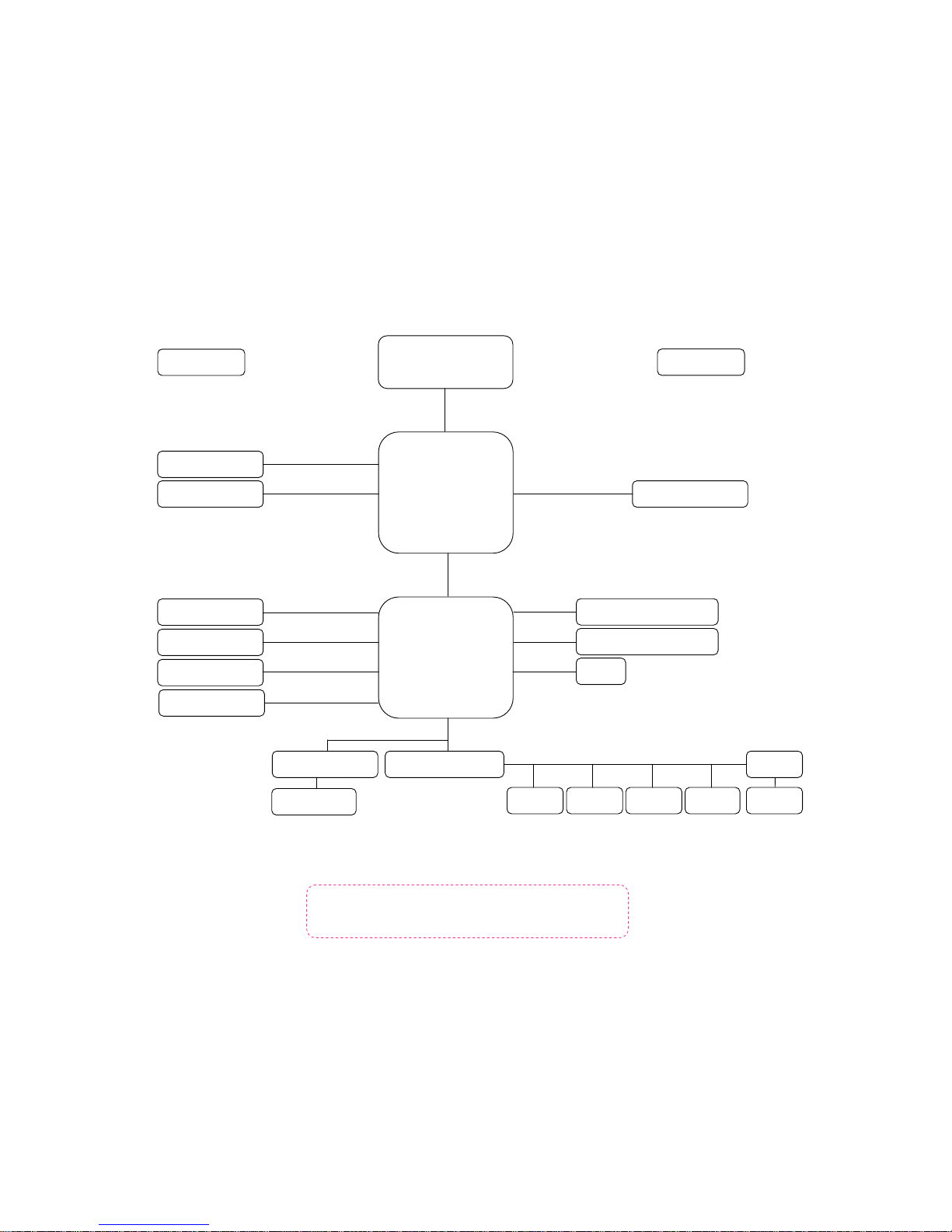
1.1 Block Diagram
Intel LGA775
Intel 945G/GC
VRD10/11
CK410
VGA
LVDS_CH7308
FSB 533/800/1066MHz
DDR2 400/533/667 MHz
DMI
S/IO W83627EHG
IDE / CF
USB x8
COM1
SPI
DIOPrinterKB/MS IrDA
LAN_RTL8102E
CODEC_ALC662
Intel ICH7
USB
SATA
LPC
PCI
SPI
DDR2(240 Pin)
SATA x2
PCI-E
SDVO
PCI
IDE
S/IO F81216D
COM3/4/5/6
HDA
COM2
MIO (Multi IO Connector)
COM1, COM2, COM3, COM4, VGA, LAN, PS2 KB/MS
Page 5

FEB-9455 User’s Manual
5
1.2 Features
System
Processor / Chipset
Processor Intel LGA775 Socket, Intel Core 2 Du o,
Pentium 4 processor in the 90 nm process
in the LGA775 Land Grid Array package or
Pentium D processor (supports 775-Land
package)
FSB 533/800 MHz (945G support 1066MHz)
Chipset Intel 945G/GC + ICH7
BIOS A WAR D 16Mb SPI
Memory
Technology DDR2 400/533/667 MHz SDRAM
Max. Capacity Up to 2GB (945G support up to 4GB)
Socket 1 x 240 DDR2 DIMM
Display
Chipset Intel 945G/GC integrated GMA950
VRAM Shared with 224MB system memory
Resolution Analog Display: Up to 2048 x 1536 (QXGA)
LVDS Chrontel CH7308 18/24 bit, Dual Channel
LVDS
Resolution
Digital LVDS: Up to 1600 x 1200 (UXGA)
Dual Display CRT + LVDS
Ethernet
Interface 10/100 Mbps ( GbE Optional)
Controller
Realtek 8102E
(Realtek RTL8111C Optional)
Audio
Interface High Definition Audio
Controller Realtek ALC662 HD CODEC
SATA
Max. Data
Transfer Rates
300 MB/s
Port 2
IDE
Mode IDE (44 Pin), Ultra A T A100/ 66/33
Channel 2
Compact Flash 1, Compact Flash Type I/II
Expansion Slot PCI 4 with Riser Card
Page 6

FEB-9455 User’s Manual
6
Internal Connector
VGA 1
LVDS 1
LAN 1
USB 2.0 8
COM
6[3(RS232), 2(RS232, supply 5V/12V),
1(RS232/422/485, supply 5V/12V)]
Parallel 1
Audio Header 1(Line-In, MIC-In)
Audio Amplifier
1 [6W(4Ω) stereo]
Compact Flash 1 (Bottom Side)
IrDA 1
PS2 1 (K/B by MCR)
Digital IO 8Bit GPIO (4 IN + 4 OUT)
Power Type ATX(8Pin)
Watchdog Timer
Interval Programmable 1~255 sec./min.
Output System reset
Environment
Operating
Temp.
-5°C~ 60°C (23°F ~ 140°F)
Stor age Temp. -20°C~ 80°C (-4°F ~ 176°F)
Relative
Humidity
0%~ 95% (non-condensing)
Form Factor
Dimension
(L x W)
203mm x 146mm
Page 7
FEB-9455 User’s Manual
7
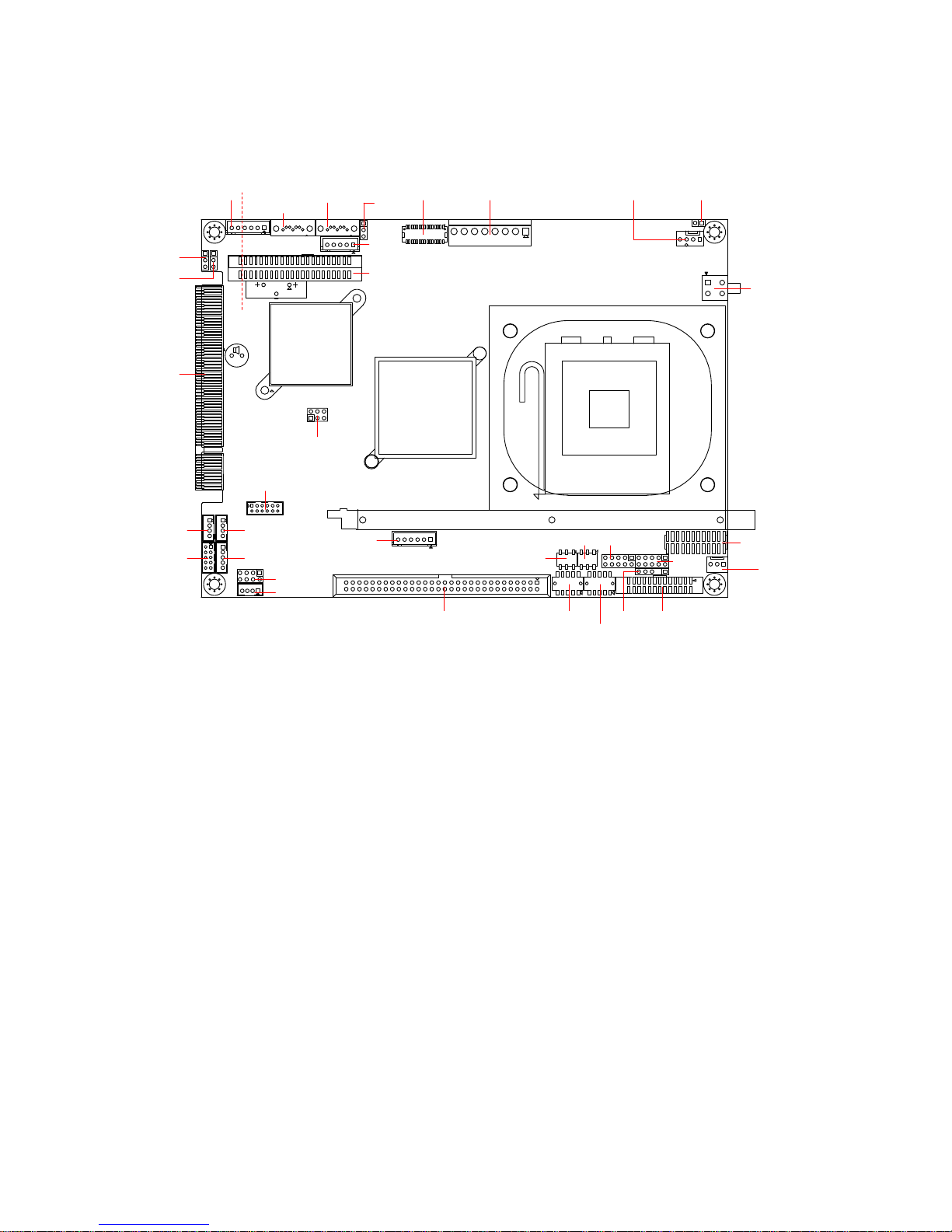
1.3 PCB Layout
5
1
1
5
14
7
14
7
1
2
43
44
6
5
1
2
1
2
12
11
8
7
1
2
1
4
4
4
12
10 9
29
30 2
1
3
4
2
8 7 6 5 4 3 2
1
1
14
13
26
1
2
9
10
1
2
9
10
1
5
2
6
1
5
26
10
2
9 1
10
2
9
1
59
60
2
1
16
1
6
JP2
JP3
SATA_PWR1
SATA1
SATA2
JP1
INV1
IDE1
LVDS1
PWR1 BT1CPUFAN1
PWR2
DIMM1
AUXFAN1
JLVDS
LAN
AUDIO2
AUDIO1
MCR1
MIO1
JP5
JP6 JFRONT1
DIO1
IR1
LPT1COM5
COM6
USB2USB1
USB3
USB4
PCI
JP4
CF1
(Bottom Side)
Page 8
FEB-9455 User’s Manual
8
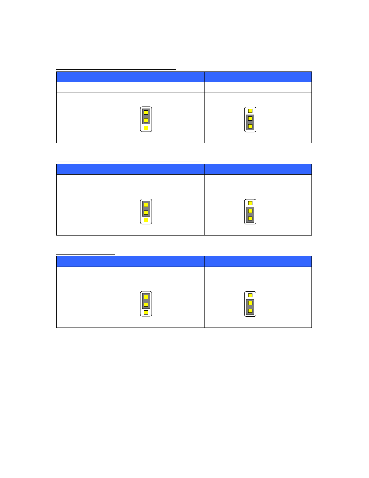
1.4 Jumper Setting
JP1:LCD Power (+3.3V / +5V) Select
Pin No. 1-2 2-3
Function LCD Power +3.3V (Default) LCD Power +5V
Jumper
Setting
JP2:Compact Flash ( Master / Slave ) Select
Pin No. 1-2 2-3
Function Master Mode Slave Mode (Default)
Jumper
Setting
JP3:CMOS Clear
Pin No. 1-2 2-3
Function Normal Operation (Default) Clear CMOS Contents
Jumper
Setting
1
2
3
1
2
3
1
2
3
1
2
3
1
2
3
1
2
3
1
2
3
1
2
3
1
2
3
1
2
3
1
2
3
1
2
3
Page 9
FEB-9455 User’s Manual
9
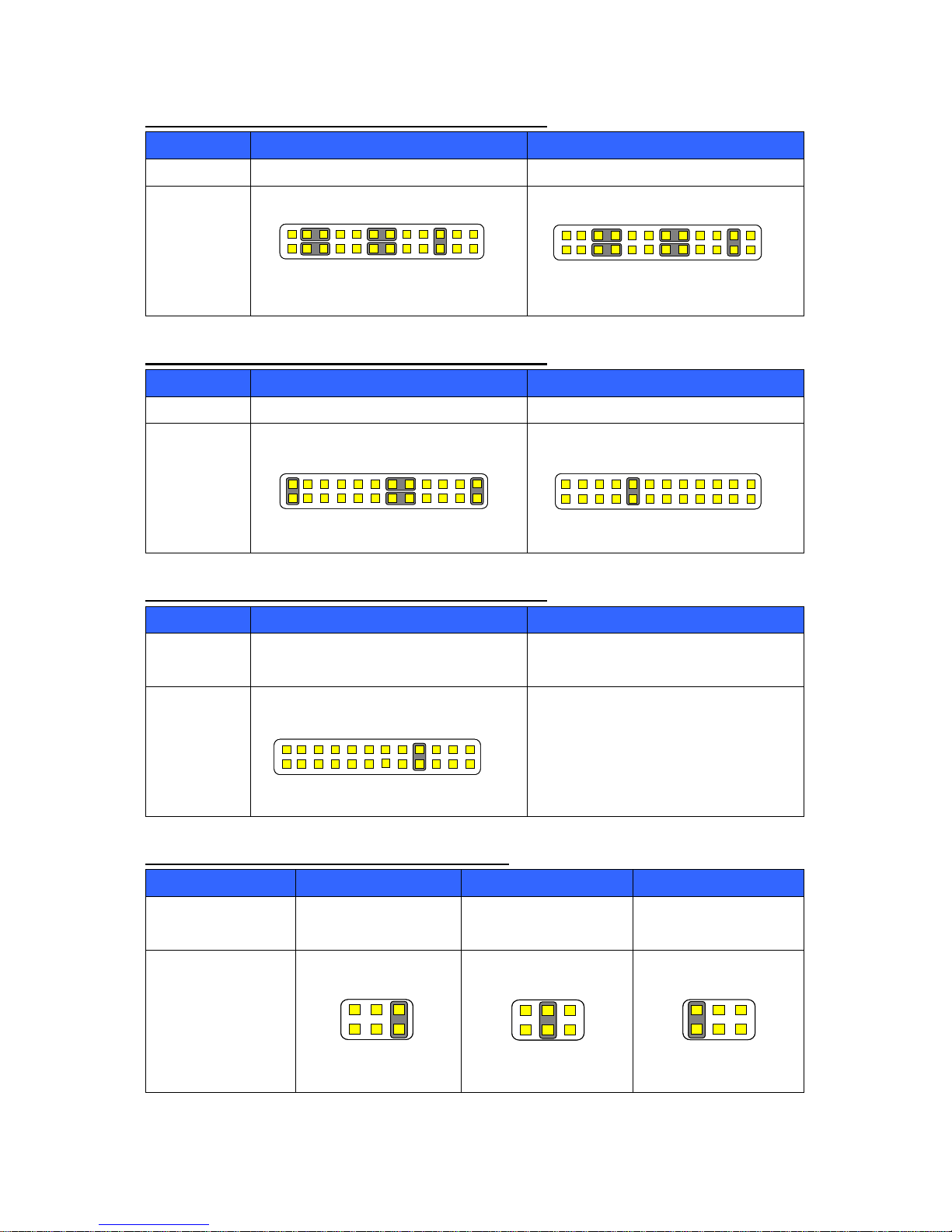
JP4:COM2 (RS-232/RS-422/RS-485) Select (1/3)
Pin No. 5-6, 11-13 , 12-14, 19-21, 20-22 3-4, 9-11, 10-12, 17-19, 18-20
Function RS-232 (Default) RS-422
Jumper
Setting
JP4:COM2 (RS-232/RS-422/RS-485) Select (2/3)
Pin No. 1-2, 9-11, 10-12, 23-24 15-16
Function RS-485 RS-422 RX 100Ω Termination
Jumper
Setting
JP4:COM2 (RS-232/RS-422/RS-485) Select (3/3)
Pin No. 7-8
Function RS-422 TX 100Ω / RS-485
Termination
Jumper
Setting
JP5 / JP6:COM5 / COM6 (5V/12V/RI) Select
Pin No. 1-2 3-4 5-6
Function +5V Modem Ring In
(Default)
+12V
Jumper Setting
6 4 2
5 3 1
6 4 2
5 3 1
6 4 2
5 3 1
6 4 2
5 3 1
6 4 2
5 3 1
6 4 2
5 3 1
23 1
24 2
23 1
24 2
23 1
24 2
23 1
24 2
23 1
24 2
23 1
24 2
23 1
24 2
23 1
24 2
23 1
24 2
23 1
24 2
Page 10

FEB-9455 User’s Manual
10
1.5 Connector Function List
Connector Function Note
AUDIO1 6W amplifier Line-out Connector
AUDIO2 Line-in, MIC-In Connector
AUXFAN1 System FAN 3-pin Connector
BT1 Power Button Connector
CF1 Compat Flash Connector
CPUFAN1 CPUFAN 4-pin Connector
COM5,COM6 Serial port Connector with Box-header
DIMM1 DDR2 240 Pin Slot
DIO1 Digital I/O with Pin-header
IDE1 HDD IDE Connector (Supply +5V)
INV1 LCD inverter Connector
IR1 IrDA Connector
MIO1 Multi IO Connector
MCR1 MSR Connector with Box-header
LAN LAN Connector with Pin-header
LPT1 Printer Connector with Pin-header
LVDS1 LVDS Connector
PCI PCI Connecting Finger
PWR1 ATX Connector with extension cable
PWR2 ATX 4 Pin Connector
SATA1, SATA2
SATA Connector
SATA_PWR1 SATA Power Connector
USB1, USB2,
USB3, USB4
USB Connector with Pin-header
Page 11
FEB-9455 User’s Manual
11
1.6 Internal Connector Pin Define
AUDIO1:Audio Amplifier Output with Box-header (2.0 mm)
Pin No. Signal
1 Audio Amplifier Out Right
2 Ground
3 Ground
4 Audio Amplifier Out Left
AUDIO2:Audio signal Connector with Pin-header (2.0 mm)
Pin No. Signal
1 MIC1-IN-L
2 LINE1-IN-L
3 MIC1-JD
4 LINE1-JD
5 Ground
6 Ground
7 MIC1-IN-R
8 LINE1-IN-R
AUXFAN1:System FAN 3 Pin Connector
Pin No. Signal
1 Ground
2 Fan Power (+12V)
3 Speed Sense
BT1:Power Button with Pin-Header (2.54mm)
Pin No. Signal
1 PSIN#
2 Ground
CPUFAN1:4Pin FAN Connector
Pin No. Signal
1 Ground
2 Fan Power (+12V)
3 Speed Sense
4 Control
Page 12
FEB-9455 User’s Manual
12
COM5, COM6:Serial Port with Box-header (2.0 mm)
Pin No. Signal Pi n No. Signal
1 DCD 2 DSR
3 RXD 4 RTS
5 TXD 6 CTS
7 DTR 8 RI/+5V/+12V
9 Ground 10 NC
DIO1:Digital I/O Connector with Pin-header (2.54mm)
Pin No. Signal Pi n No. Signal
1 DIO-Out3 2 DIO-In3
3 DIO-Out2 4 DIO-In2
5 DIO-Out1 6 DIO-In1
7 DIO-Out0 8 DIO-In0
9 Ground 10 +5V
Page 13
FEB-9455 User’s Manual
13
IDE1:HDD IDE Connector with Box-header (2.0mm)
Pin No. Signal Pin No. Signal
1 RESET# 2 Ground
3 Data 7 4 Data 8
5 Data 6 6 Data 9
7 Data 5 8 Data 10
9 Data 4 10 Data 11
11 Data 3 12 D at a 12
13 Data 2 14 Data 13
15 Data 1 16 Data 14
17 Data 0 18 Data 15
19 Ground 20 NC
21 DMA REQ 22 Ground
23 IOW# 24 Ground
25 IOR# 26 Ground
27 IOCHRDY 28 Pull-down
29 DMA ACK# 30 Ground
31 INT REQ 32 NC
33 SA1 34 P66DETECT
35 SA0 36 SA2
37 HDC CS1# 38 HDC CS3#
39 HDD Active# 40 Ground
41 +5V 42 +5V
43 Ground 44 NC
INV1:Inverter Connector with Box header (2.50 mm)
Pin No. Signal
1 +12V
2 +12V
3 Ground
4 Ground
5 Inverter Enable
Page 14

FEB-9455 User’s Manual
14
IR1:IR Connector with Pin-header (2.54 mm)
Pin No. Signal
1 +5V
2 NC
3 IR-RX
4 Ground
5 IR-TX
LAN:LAN Connector with Box-header (2.0 mm)
Pin No. Signal Pi n No. Signal
1 L_MDI0+ 2 L_MDI03 L_MDI1+ 4 L_MDI15 L_P4&P5C 6 L_P7&P8C
7 L_MDI2+ 8 L_MDI29 L_MDI3+ 10 L_MDI3-
11 LED1# 12 LED0#
LPT1:Parallel Port Connector with Box-header (2.0 mm)
Pin No. Signal Pin No. Signal
1 Strobe# 14 Auto Form Feed#
2 Data 0 15 Error#
3 Data 1 16 Initialization#
4 Data 2 17 Printer Select IN#
5 Data 3 18 Ground
6 Data 4 19 Ground
7 Data 5 20 Ground
8 Data 6 21 Ground
9 Data 7 22 Ground
10 Acknowledge# 23 Ground
11 Busy 24 Ground
12 Paper Empty 25 Ground
13 Printer Select 26 Ground
Page 15

FEB-9455 User’s Manual
15
LVDS1:LVDS Panel Signal with Wafer Con nect o r (1.2 5 mm)
Pin No. Signal Pin No. Signal
1 Ground 2 Ground
3 L_DC3 4 L_DC35 L_CLK0 6 L_CLK07 L_DC2 8 L_DC29 L_DC1 10 L_DC1-
11 L_DC0 12 L_DC013 Ground 14 Ground
15
L_DC7
16
L_DC7
17
L_CLK1
18
L_CLK1
19 L_DC6 20 L_DC6
21
L_DC5
22
L_DC5
23
L_DC4
24
L_DC4
25 Ground 26 Ground
27 LVDS Power 28 L VD S Power
29 LVDS Power 30 L VD S Power
Note:LVDS Power = +5V or +3.3V (Default)
Page 16

FEB-9455 User’s Manual
16
MIO1:Multi-IO Connector with Box-header (2.54 mm)
Pin No. Signal Pin No. Signal
1 DCD#4 2 DSR#4
3 RXD#4 4 RTS#4
5 TXD#4 6 CTS#4
7 DTR#4 8 RI#4
9 DCD#3 10 DSR#3
11 RXD#3 12 RTS#3
13 TXD#3 14 CTS#3
15
DTR#3
16
RI#3
17
DCD#2/DT-
18
DSR#2
19 RXD#2/DT+ 20 RTS#2
21
TXD#2/422R+
22
CTS#2
23
DTR#2/422R-
24
RI#2
25 DCD#1 26 DSR#1
27 RXD#1 28 RTS#1
29 TXD#1 30 CTS#1
31 DTR#1 32 RI#1
33 F_KCLK 34 F_KDAT
35 L_MCLK 36 L_MDAT
37 DIO_OUT0# 38 DIO_IN0
39 L_TX- 40 L_TX+
41 L_P4&P5C 42 L_RX43 L_RX+ 44 L_P7&P8C
45 LED0# 46 LED1#
47 5VHSYNC 48 5VVSYNC
49 5VDDCCLK 50 5VDDCDATA
51 Ground 52 VGA_RED
53 Ground 54 VGA_GREEN
55 Ground 56 VGA_BLUE
57 Ground 58 HDD_LED#
59 FA-OUT-L 60 FA-OUT-R
Page 17
FEB-9455 User’s Manual
17
MCR1:External Keyboard Connector with Pin-header (2.5 mm)
Pin No. Signal Pi n No. Signal
1 Ground 2 KDAT_CON
3 KDAT_KBC 4 KCLK_CON
5 KCLK_KBC 6 +5V
PWR1:ATX 8-pin Connector (Expansion cable) with Pin-header
Pin No. Signal Pi n No. Signal
1 +5V 2 +5V
3 5VSB 4 +12V
5 PS_ON- 6 Ground
7 Ground 8 Ground
PWR2:ATX 12V 4-pin Connector
Pin No. Signal
1 Ground
2 Ground
3 +12V
4 +12V
SATA_PWR1:SATA 6pin Power Connector with Box-header (2.5 mm)
Pin No. Signal Pi n No. Signal
1 +5V 2 +5V
3 Ground 4 Ground
5 +12V 6 +12V
USB1:USB0 Port Connector with Pin-header (2.0mm)
Pin No. Signal
1 USB Power (+5V)
2 USB DATA03 USB DATA0+
4 Ground
Page 18
FEB-9455 User’s Manual
18
USB2:USB1 Port Connector with Pin-header (2.0mm)
Pin No. Signal
1 USB Power (+5V)
2 USB DATA13 USB DATA1+
4 Ground
USB3:USB2, USB3, USB4, USB5 Port Connector with Pin-head er (2.0mm)
Pin No. Signal Pi n No. Signal
1 USB DATA2- 2 USB DATA43 USB DATA2+ 4 USB DATA4+
5 Ground 6 Ground
7 USB DATA3- 8 USB DATA59 USB DATA3+ 10 USB DATA5+
USB4:USB6, USB7 Port Connector with Pin-header (2.0mm)
Pin No. Signal
1 USB DATA62 USB DATA6+
3 Ground
4 USB DATA75 USB DATA7+
Page 19
FEB-9455 User’s Manual
19
Chapter 2 BIOS Setup
This chapter introduces BIOS setup information.
Power on or reboot the system board, when screen appear
“Press DEL to enter SETUP“, Press <DEL> key to run BIOS SETUP Utility.
Note: The BIOS configuration for reference only, may subject to change without prior
notice.
2.1 Main Menu
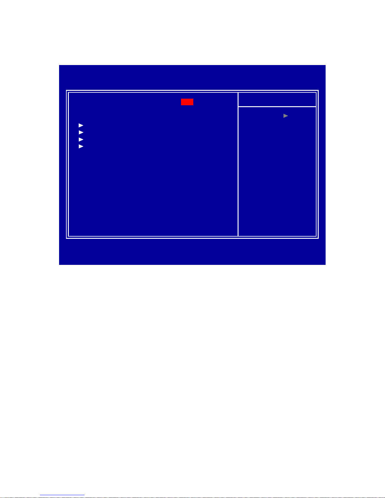
Please use arrow keys to select item, then press <Enter> key to accept or enter the
sub-menu.
Phoenix – AwardBIOS CMOS Setup Utility
Frequency / Voltage Control
Load Fail-Safe Defaults
Load Optimized Defaults
Set Supervisor Password
Set User Password
Save & Exit Setup
Exit Without Saving
Esc : Quit
↑↓ ← →
: Select Item
F10 : Save & Exit Setup
Time, Date, Hard Disk Type…
Standard CMOS Features
Advanced BIOS Features
Advanced Chipset Features
Integrated Peripherals
Power Management Setup
PnP/PCI Configurations
PC Health Status
Page 20
FEB-9455 User’s Manual
20
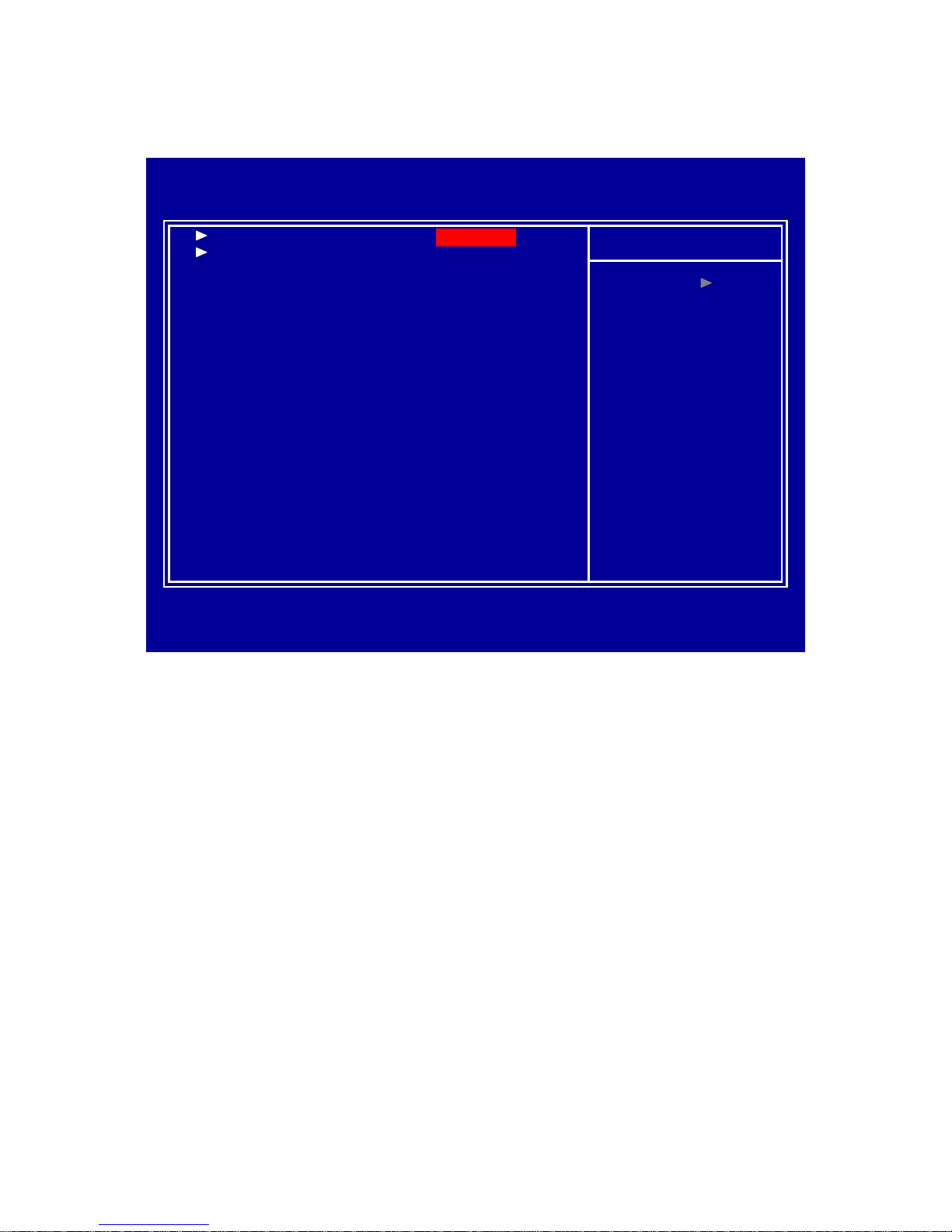
2.2 Standard CMOS Features
Phoenix – AwardBIOS CMOS Setup Utility
Standard CMOS Features
Item Help
↑↓ ←→
:Move Enter:Select +/-/PU/PD:Value F10:Save ESC:Exit F1: General Help
IDE Channel 0 Master [ None ]
IDE Channel 0 Slave [ None ]
IDE Channel 1 Master [ None ]
IDE Channel 1 Slave [ None ]
Video [ EGA / VGA ]
Halt On [ No Errors ]
Base Memory 640K
Extended Memory 514048K
Total Memory 515072K
Menu Level
Change the day, month,
year and century
Date (mm:dd:yy) Tue. Aug 18 2009
Time (hh:mm:ss) 16 : 8 : 20
F5: Previous Values F6: Fail-Safe Defaults F7: Optimized Defaults
□ Date
Set system date.
□ Time
Set system time.
□ IDE Channel 0/1, Master/Slave
Press <Enter> for IDE devi ce automatic detection.
□ Video
Select Video device type.
□ Halt on
Select stop procedure or ignore when error detected during POST (Power On Self
Test).
Page 21
FEB-9455 User’s Manual
21
2.3 Advanced BIOS Features
Item Help
Menu Level
↑↓ ←→
:Move Enter:Select +/-/PU/PD:Value F10:Save ESC:Exit F1: General Help
CPU Feature
Hard Disk Boot Priority
Virus Warning
CPU L1 & L2 Cache
CPU L3 Cache
Quick Power On Self Test
First Boot Device
Second Boot Device
Third Boot Device
Boot Other Device
Boot Up NumLock Status
Gate A20 Option
Typematic Rate Setting
Typematic Rate (Chars/Sec)
Typematic Delay (Msec)
Security Option
OS Select For DRAM > 64MB
Small Logo(EPA) Show
x
x
Phoenix – AwardBIOS CMOS Setup Utility
Advanced BIOS Features
F5: Previous Values F6: Fail-Safe Defaults F7: Optimized Defaults
[ Press Enter ]
[ Press Enter ]
[ Disabled ]
[ Enabled ]
[ Enabled ]
[ Enabled ]
[ USB-CDROM ]
[ Hard Disk ]
[ USB-FDD ]
[ Enabled ]
[ On ]
[ Fast ]
[ Disabled ]
6
250
[ Setup ]
[ Non-OS2 ]
[ Disabled ]
□ CPU Feature
Press <Enter> to select CPU parameter.
□ Hard Disk Boot Priority
Press <Enter> to select Hard Disk boot device priority.
□ Virus Warning
Select “Virus W a rning ” Enabled/Disabled.
□ CPU L1 & L2 Cache
Select “CPU L1 & L2 Cache” Enabled/Disabled.
□ CPU L3 Cache
Select “CPU L3 Cache” Enabled/Disabled.
Page 22

FEB-9455 User’s Manual
22
□ Quick Power On Self Test
Select “Quick Power On Self Test” Enabled/Disabled.
□ First/Second/Third Boot Device
Select boot device priority.
□ Boot Other Device
Select “Boot Other Device” Enabled/Disabled.
□ Boot Up NumLock Status
Select <NumLock> key ON/Off when system boot up.
□ Gate A20 Option
Select Gate A20 controlled by Keyboard controller (Normal) or Port 92 (Fast).
□ Typematic Rate Setting
Select “Typematic Rate Setting” Enabled to set,
Typematic Rate (Chars/Sec): Number of characters repeated in one second.
Typematic Delay (Msec): When holding one key, set the time between the first and
second character displayed.
□ Security Option
Select security mode,
Setup: Require password to permit BIOS setup utility.
System: Require password to permit boot-up and BIOS setup utility.
□ OS Select For DRAM > 64M
Select “OS2” only if yo u are runni ng older v er sion o f IBM OS/2 Operating System with
greater than 64MB of RAM on the system. Otherwise select “Non-OS/2” setting.
□ Small Logo(EPA) Show
Select EPA (Environmental Protection Agency) Energy Star logo appears during the
system boot-up process.
Page 23
FEB-9455 User’s Manual
23
2.4 Advanced Chipset Features
Item Help
Menu Level
↑↓ ←→
:Move Enter:Select +/-/PU/PD:Value F10:Save ESC:Exit F1: General Help
DRAM Timing Selectable
CAS Latency Time
DRAM RAS# to CAS# Delay
DRAM RAS# Precharge
Precharge delay (tRAS)
System Memory Frequency
System BIOS Cacheable
Video BIOS Cacheable
** VGA Setting **
PEG/Onchip VGA Control
On-Chip Frame Buffer Size
DVMT Mode
DVMT / Fixed Memory Size
Boot Display
Panel Number
Phoenix – AwardBIOS CMOS Setup Utility
Advanced Chipset Features
x
x
x
x
x
[ Auto ]
[ 8MB ]
[ DVMT ]
[ 128MB ]
[ Auto ]
[ 800x600-18 LVDS ]
F5: Previous Values F6: Fail-Safe Defaults F7: Optimized Defaults
[ By SPD ]
Auto
Auto
Auto
Auto
Auto
[ Enabled ]
[ Disabled ]
□ DRAM Timing Selectable
Select DRAM timing by SPD (Serial Presence Detect) or manual.
□ System BIOS Cacheable
Select Enabled to caching of the system BIOS at F0000h-FFFFFh, resulting in better
system performance. However, if any program is written to this memory area, the
system error may result.
□ Video BIOS Cacheable
Select Enabled to caching of the video BIOS at C0000h-F7FFFh, resulting in better
video performance. However, if any program is written to this memory area, the
system error may result.
□ PEG/Onchip VGA Control
Select VGA control by PEG (PCI-Express Graphic) or onb oar d c hi pset.
Page 24

FEB-9455 User’s Manual
24
□ On-Chip Frame Buffer Size
Select share system memory 1MB or 8MB.
□ DVMT Mode
DVMT (Dynamic Video Memory Technology) allowing the system to dynamically
allocate memory resources according to the demands of the system at any point in
time, that improve efficiency of the memory allocated to either system or graphics
processor.
□ DVMT/Fixed Memory Size
Select DVMT/Fixed Memory Size 64MB/128MB/224MB.
□ Boot Display
Select boot display device type.
□ Panel Number
Select LCD panel type.
Page 25
FEB-9455 User’s Manual
25
2.5 Integrated Peripherals
Item Help
Menu Level
↑↓ ←→
:Move Enter:Select +/-/PU/PD:Value F10:Save ESC:Exit F1: General Help
OnChip IDE Device
Onboard Device
Super IO Device
Watch Dog Timer Select
Onboard Serial Port 3
Serial Port 3 Use IRQ
Onboard Serial Port 4
Serial Port 4 Use IRQ
Onboard Serial Port 5
Serial Port 5 Use IRQ
Onboard Serial Port 6
Serial Port 6 Use IRQ
USB Device Setting
Phoenix – AwardBIOS CMOS Setup Utility
Integrated Peripherals
[ Press Enter ]
[ Press Enter ]
[ Press Enter ]
[ Disabled ]
[ 3E8 ]
[ IRQ10 ]
[ 2E8 ]
[ IRQ11 ]
[ 4F8 ]
[ IRQ10 ]
[ 4E8 ]
[ IRQ11 ]
[ Press Enter ]
F5: Previous Values F6: Fail-Safe Defaults F7: Optimized Defaults
Page 26
FEB-9455 User’s Manual
26
□ OnChip IDE Device
Press <Enter> to set IDE and SATA device configuration.
Item Help
Menu Level
↑↓ ←→
:Move Enter:Select +/-/PU/PD:Value F10:Save ESC:Exit F1: General Help
IDE HDD Block Mode
IDE DMA transfer access
On-Chip Primary PCI IDE
IDE Primary Master PIO
IDE Primary Slave PIO
IDE Primary Master UDMA
IDE Primary Slave UDMA
On-Chip Secondary PCI IDE
IDE Secondary Master PIO
IDE Secondary Slave PIO
IDE Secondary Master UDMA
IDE Secondary Slave UDMA
*** On-Chip Serial ATA Setting ***
On-Chip Serial ATA
SATA PORT Speed Settings
PATA IDE Mode
SATA Port
Phoenix – AwardBIOS CMOS Setup Utility
OnChip IDE Device
If your IDE hard drive
supports block mode
select Enabled for
automatic detection of
the optimal number of
block read/writes per
sector the drive can
support
F5: Previous Values F6: Fail-Safe Defaults F7: Optimized Defaults
[ Enabled ]
[ Enabled ]
[ Enabled ]
[ Auto ]
[ Auto ]
[ Auto ]
[ Auto ]
[ Enabled ]
[ Auto ]
[ Auto ]
[ Auto ]
[ Auto ]
[ Combined Mode ]
Disabled
[ Secondary ]
P0,P2 is Primary
x
Page 27
FEB-9455 User’s Manual
27
□ Onboard Device
Press <Enter> to select Az alia/AC97 Auto/All Disabled.
Item Help
Menu Level
↑↓ ←→
:Move Enter:Select +/-/PU/PD:Value F10:Save ESC:Exit F1: General Help
Azalia/AC97 Audio Select
Phoenix – AwardBIOS CMOS Setup Utility
Onboard Device
F5: Previous Values F6: Fail-Safe Defaults F7: Optimized Defaults
[ Auto ]
Page 28
FEB-9455 User’s Manual
28
□ Super IO Device
Press <Enter> to select Serial, Parallel and “PWRON After PWR-Fail” configuration.
Item Help
Menu Level
↑↓ ←→
:Move Enter:Select +/-/PU/PD:Value F10:Save ESC:Exit F1: General Help
Onboard Serial Port 1
Onboard Serial Port 2
UART Mode Select
x RxD , TxD Active
x IR Transmission Delay
x UR2 Duplex Mode
x Use IR Pins
Onboard Parallel Port
Parallel Port Mode
x EPP Mode Select
x ECP Mode Use DMA
PWRON After PWR-Fail
Phoenix – AwardBIOS CMOS Setup Utility
Super IO Device
F5: Previous Values F6: Fail-Safe Defaults F7: Optimized Defaults
[ 3F8/IRQ4 ]
[ 2F8/IRQ3 ]
[ Normal ]
Hi , Lo
Enabled
Half
IR-Rx2Tx2
[ 378/IRQ7 ]
[ SPP ]
EPP1.7
3
[ Off ]
□ Watch Dog T i mer Sel e ct
Select Watch dog Disabled or set timer value.
□ Onboard Serial Port 3/4/5/6
Select serial port addr ess
□ Serial Port 3/4/5/6 Use IRQ
Select serial port IRQ
Page 29
FEB-9455 User’s Manual
29
□ USB Device Setting
Press <Enter> to select USB device configuration.
Item Help
Menu Level
↑↓ ←→
:Move Enter:Select +/-/PU/PD:Value F10:Save ESC:Exit F1: General Help
Phoenix – AwardBIOS CMOS Setup Utility
USB Device Setting
[Enable] or [Disable]
Universal Host
Controller Interface
for Universal Serial
Bus.
USB 1.0 Controller
USB 2.0 Controller
USB Operation Mode
USB Keyboard Function
USB Mouse Function
USB Storage Function
*** USB Mass Storage Device Boot Setting ***
[ Enabled ]
[ Enabled ]
[ High Speed ]
[ Enabled ]
[ Enabled ]
[ Enabled ]
F5: Previous Values F6: Fail-Safe Defaults F7: Optimized Defaults
Page 30
FEB-9455 User’s Manual
30
2.6 Power Management Setup
Item Help
Menu Level
↑↓ ←→
:Move Enter:Select +/-/PU/PD:Value F10:Save ESC:Exit F1: General Help
PCI Express PM Function
ACPI Function
ACPI Suspend Type
Run VGABIOS if S3 Resume
Power Management
Video Off Method
Video Off In Suspend
Suspend Type
Suspend Mode
HDD Power Down
Soft-Off by PWR-BTTN
Power On by Ring
Resume by Alarm
Date(of Month) Alarm
Time(hh:mm:ss) Alarm
** Reload Global Timer Events **
Primary IDE 0
Primary IDE 1
Secondary IDE 0
Secondary IDE 1
FDD, COM, LPT Port
PCI PIRQ[A-D]#
Phoenix – AwardBIOS CMOS Setup Utility
Power Management Setup
x
x
x
F5: Previous Values F6: Fail-Safe Defaults F7: Optimized Defaults
▲
▼
[ Press Enter ]
[ Enabled ]
S1(POS)
Auto
[ User Define ]
[ DPMS]
[ Yes ]
[ Stop Grant ]
[ Disabled ]
[ Disabled ]
[ Instant-Off ]
[ Disabled ]
[ Disabled ]
0
0 : 0 : 0
[ Disabled ]
[ Disabled ]
[ Disabled ]
[ Disabled ]
[ Disabled ]
[ Disabled ]
Page 31

FEB-9455 User’s Manual
31
□ PCI Express PM Function
Press <Enter> to select “Wake-up by LAN” Enabled/Disabled.
Item Help
Menu Level
↑↓ ←→
:Move Enter:Select +/-/PU/PD:Value F10:Save ESC:Exit F1: General Help
Wake-up by LAN
Phoenix – AwardBIOS CMOS Setup Utility
PCI Express PM Function
[ Disabled ]
F5: Previous Values F6: Fail-Safe Defaults F7: Optimized Defaults
□ ACPI Function
Select ACPI (Advanced Configuration and Power Management) Enabled/Disabled.
□ Power Management
Select power saving type.
□ Video Off Method
There are three methods,
Blank Screen: Writes blanks to the video buffer.
V/H SYNC + Blank: Turn off the vertical and horiz ontal sync. ports a nd write blanks to
the video buffer.
DPMS: The DPMS (Display Power Management Signaling) allows BIOS control the
video display.
Page 32

FEB-9455 User’s Manual
32
□ Video Off In Suspend
Select Video On/Off during suspend state.
□ Suspend Type
There are two types,
Stop Grant: CPU goes into idle mode during suspend state.
PwrOn Suspend: CPU and system remain powered on during suspend state.
□ Suspend Mode
Select the time of system inactivity, all devices except the CPU will be shut off.
□ HDD Power Down
Select time of system inactivity, the hard disk drive will be powered down while all
other devices remain active.
□ Soft-O ff by PWR_BTTN
Select power button functi on,
Instant-off: Press power button will power off instantly.
Delay 4 Sec: Press power button 4 second to power off.
□ Power On by Ring
Select Power on by Ring Indicator sig nal fro m Mod em.
□ Resume by Alarm
Set date and time to power on system from soft-off stat e.
□ Primary/Secondary IDE 0/1
Select IDE Enabled/Disabled
□ FDD, COM, LPT Port
Select FDD, Serial and Printer port Enabled/Disabled
□ PCI PIRQ[A-D]#
Select PCI PIRQ[A-D] Enabled/Disabl ed
Page 33
FEB-9455 User’s Manual
33
2.7 PnP/PCI Configurations
Item Help
↑↓ ←→
:Move Enter:Select +/-/PU/PD:Value F10:Save ESC:Exit F1: General Help
Reset Configuration Data
Resources Controlled By
IRQ Resources
Phoenix – AwardBIOS CMOS Setup Utility
PnP / PCI Configurations
x
[ Disabled ]
[ Auto(ESCD) ]
Press Enter
F5: Previous Values F6: Fail-Safe Defaults F7: Optimized Defaults
Menu Level
Default is Disabled.
Select Enabled to
reset Extended System
Configuration Data
ESCD) when you exit
Setup if you have
installed a new add-on
and the system
reconfiguration has
caused such a serious
conflict that the OS
cannot boot
□ Reset Configuration Data
Select Enabled to reset Extended System Configuration Data (ESCD) when you exit
BIOS setup utility, if you have installed new add-on card and the system
reconfiguration has caused such a serious conflict that the OS cannot boot.
□ Resources Controlled By
BIOS can automatically configure all the boot and Plug and Play compatible devices.
If you choose Auto, you cannot select IRQ DMA and memory base address fields,
since BIOS automatically assigns them.
Page 34
FEB-9455 User’s Manual
34
2.8 PC Health Status
Item Help
Menu Level
↑↓ ←→
:Move Enter:Select +/-/PU/PD:Value F10:Save ESC:Exit F1: General Help
Shutdown Temperature
CPU Warning Temperature
Current System Temperature
Current CPU Temperature
CPU Fan Speed
SYS. Fan Speed
Vcore
+12 V
+1.5 V
+1.8 V
+5 V
+3.3 V
VBAT (V)
3.3VSB (V)
** Smart FAN Setup **
CPU Fan Temperature
System Fan Temperature
Phoenix – AwardBIOS CMOS Setup Utility
PC Health Status
F5: Previous Values F6: Fail-Safe Defaults F7: Optimized Defaults
[ Disabled ]
[ Disabled ]
56℃/ 132
℉
54℃/ 131
℉
1454 RPM
0 RPM
1.30 V
12.14 V
1.50 V
1.82 V
4.90 V
3.37 V
3.05 V
3.34 V
[ 55℃/131℉]
[ 50℃/122℉]
□ Shutdown Temperature
If CPU temperature reaches the setting value will automatic shutdown system.
□ CPU Warning Temperature
If CPU temperature reaches the setting value will beep in DOS mode.
□ CPU/System Fan Temperature
Setup CPU/System Smart FAN temperature.
Page 35
FEB-9455 User’s Manual
35
2.9 Frequency/Voltage Control
Item Help
Menu Level
↑↓ ←→
:Move Enter:Select +/-/PU/PD:Value F10:Save ESC:Exit F1: General Help
CPU Clock Ratio
Spread Spectrum
Phoenix – AwardBIOS CMOS Setup Utility
Frequency / Voltage Control
F5: Previous Values F6: Fail-Safe Defaults F7: Optimized Defaults
[ 9 X ]
[ Disabled ]
□ CPU Clock Ratio
Select “CPU Clock Ratio” (From 6 to 9).
□ Spread Spectrum
Select “S pr e ad Spectrum” Enabled/Disabled.
Page 36
FEB-9455 User’s Manual
36
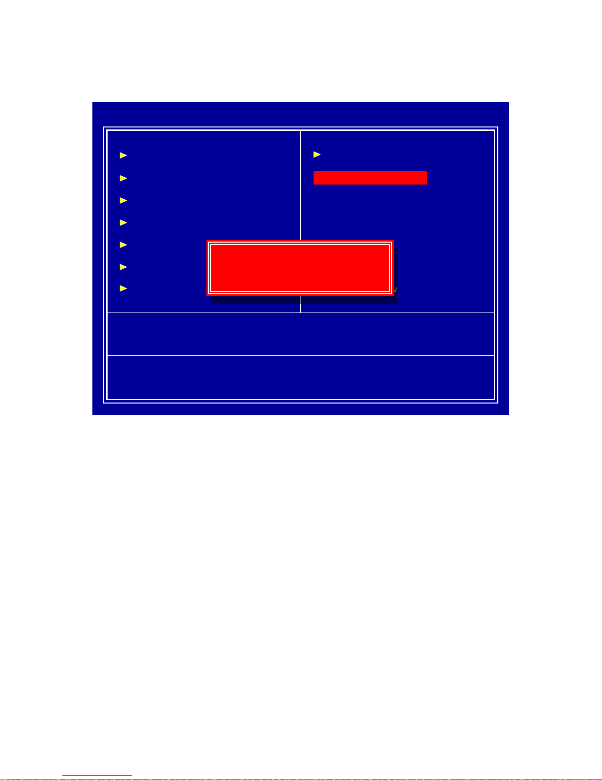
2.10 Load Fail-Safe Defaults
Frequency / Voltage Control
Load Fail-Safe Defaults
Load Optimized Defaults
Set Supervisor Password
Set User Password
Save & Exit Setup
Exit Without Saving
Phoenix – AwardBIOS CMOS Setup Utility
Esc : Quit
↑↓ ← →
: Select Item
F10 : Save & Exit Setup
Time, Date, Hard Disk Type…
Standard CMOS Features
Advanced BIOS Features
Advanced Chipset Features
Integrated Peripherals
Power Management Setup
PnP/PCI Configurations
PC Health Status
Load Fail-Safe Defaults (Y/N)? N
Load Fail-Safe Defaults (Y/N)? N
This item will set configuration for non optimiz ed system operation.
Page 37
FEB-9455 User’s Manual
37
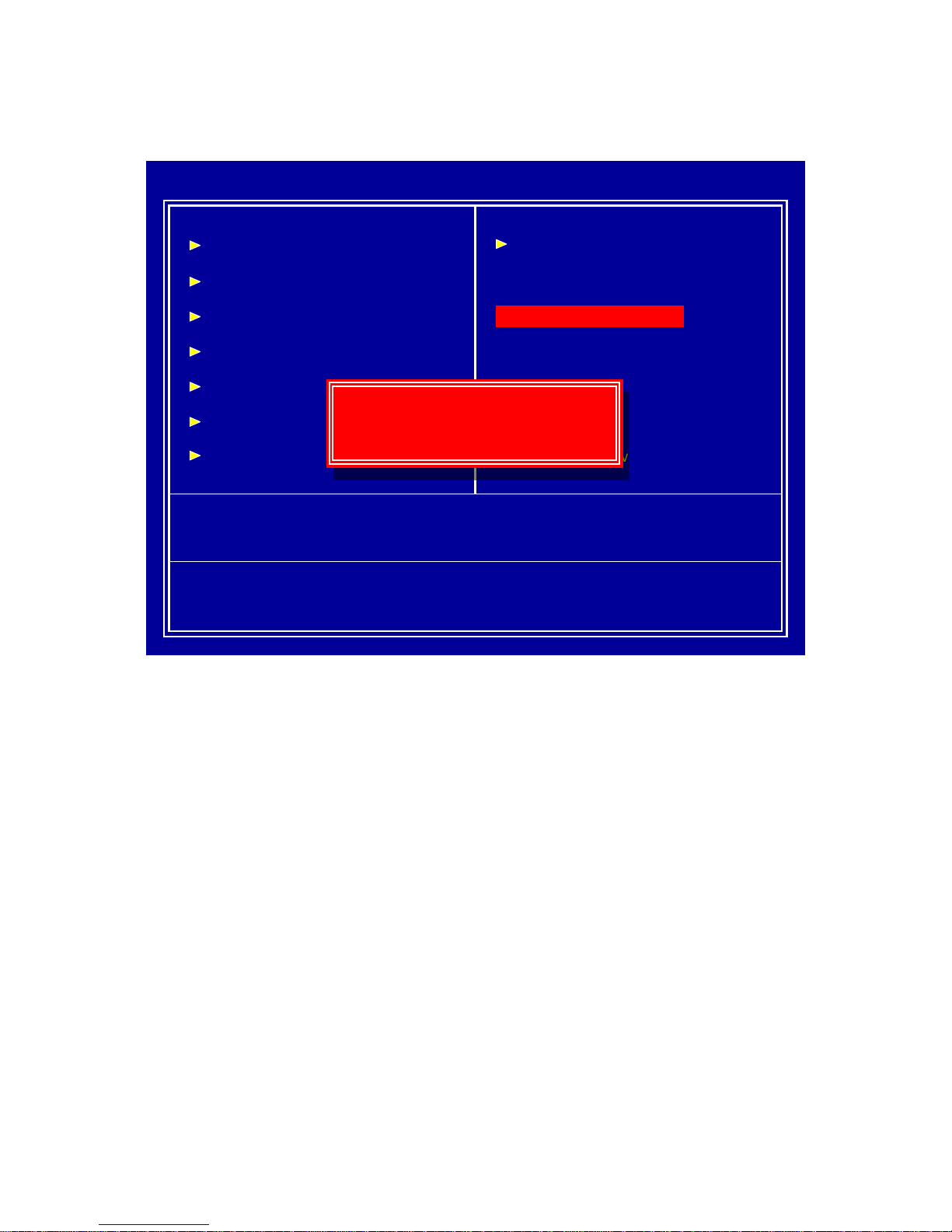
2.11 Load Optimized Defaults
Phoenix – AwardBIOS CMOS Setup Utility
Frequency / Voltage Control
Load Fail-Safe Defaults
Load Optimized Defaults
Set Supervisor Password
Set User Password
Save & Exit Setup
Exit Without Saving
Esc : Quit
↑↓ ← →
: Select Item
F10 : Save & Exit Setup
Time, Date, Hard Disk Type…
Standard CMOS Features
Advanced BIOS Features
Advanced Chipset Features
Integrated Peripherals
Power Management Setup
PnP/PCI Configurations
PC Health Status
Load Optimized Defaults (Y/N)? N
Load Optimized Defaults (Y/N)? N
This item will restore factory default setting for optimized system operation.
Page 38
FEB-9455 User’s Manual
38
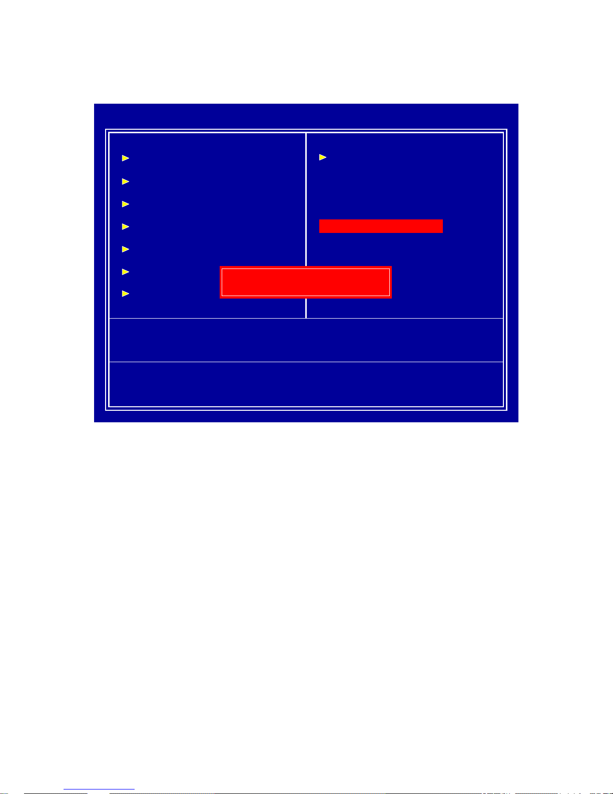
2.12 Set Supervisor Password
Phoenix – AwardBIOS CMOS Setup Utility
Frequency / Voltage Control
Load Fail-Safe Defaults
Load Optimized Defaults
Set Supervisor Password
Set User Password
Save & Exit Setup
Exit Without Saving
Esc : Quit
↑↓ ← →
: Select Item
F10 : Save & Exit Setup
Time, Date, Hard Disk Type…
Standard CMOS Features
Advanced BIOS Features
Advanced Chipset Features
Integrated Peripherals
Power Management Setup
PnP/PCI Configurations
PC Health Status
Enter Password:
If set supervisor password, it will request typing password to enter BIOS setup utility.
Page 39
FEB-9455 User’s Manual
39
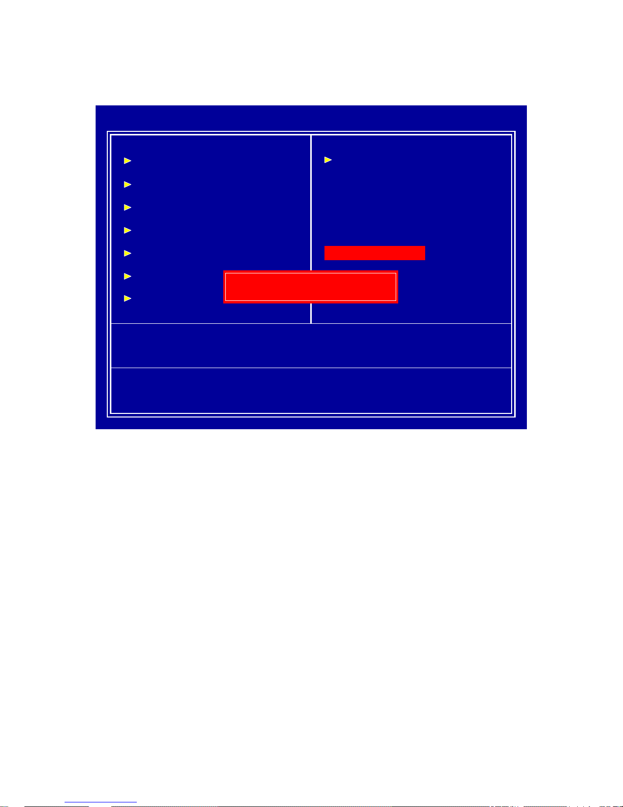
2.13 Set User Password
Phoenix – AwardBIOS CMOS Setup Utility
Frequency / Voltage Control
Load Fail-Safe Defaults
Load Optimized Defaults
Set Supervisor Password
Set User Password
Save & Exit Setup
Exit Without Saving
Esc : Quit
↑↓ ← →
: Select Item
F10 : Save & Exit Setup
Time, Date, Hard Disk Type…
Standard CMOS Features
Advanced BIOS Features
Advanced Chipset Features
Integrated Peripherals
Power Management Setup
PnP/PCI Configurations
PC Health Status
Enter Password:
If set user p assw ord w ill req uest ty ping p assw ord to enter BIO S set u p utili ty, and does
not allowed to modi fy con fig ur ati on .
Page 40
FEB-9455 User’s Manual
40
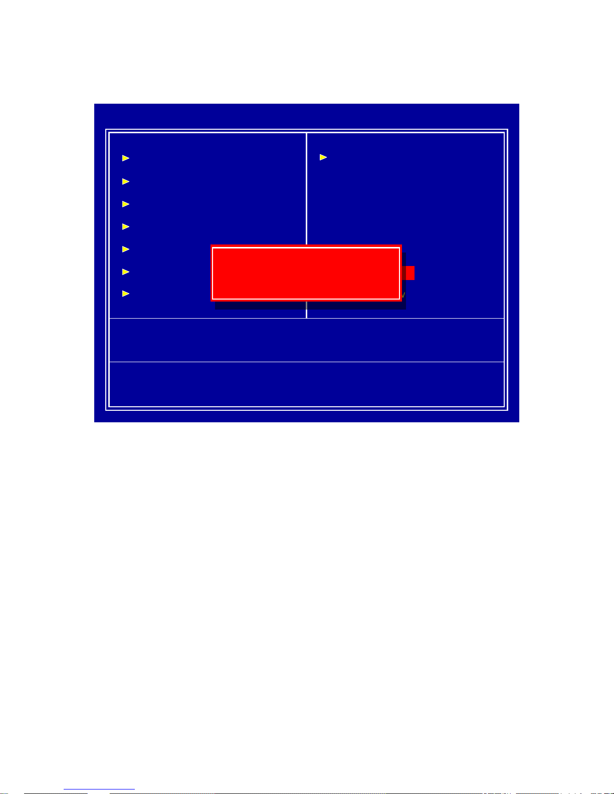
2.14 Save & Exit Setup
Frequency / Voltage Control
Load Fail-Safe Defaults
Load Optimized Defaults
Set Supervisor Password
Set User Password
Save & Exit Setup
Exit Without Saving
Phoenix – AwardBIOS CMOS Setup Utility
Esc : Quit
↑↓ ← →
: Select Item
F10 : Save & Exit Setup
Time, Date, Hard Disk Type…
Standard CMOS Features
Advanced BIOS Features
Advanced Chipset Features
Integrated Peripherals
Power Management Setup
PnP/PCI Configurations
PC Health Status
SAVE to CMOS and EXIT (Y/N)? Y
SAVE to CMOS and EXIT (Y/N)? Y
This item confirm save configuration or not be f or e exit BIOS setup utility,
Press <Y> and <Enter> to save configuration, then reboot system.
Press <N> and <Enter> will back to BIOS setup utility.
Page 41
FEB-9455 User’s Manual
41
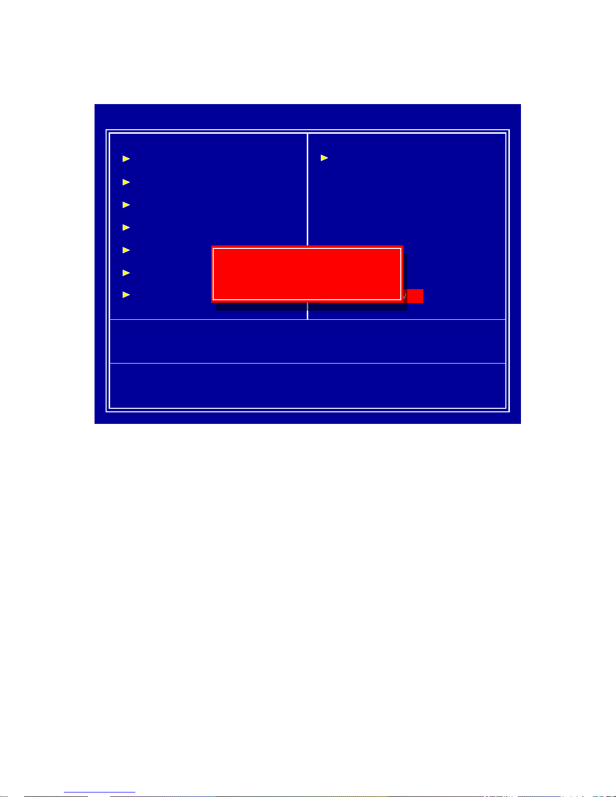
2.15 Exit Without Saving
Frequency / Voltage Control
Load Fail-Safe Defaults
Load Optimized Defaults
Set Supervisor Password
Set User Password
Save & Exit Setup
Exit Without Saving
Phoenix – AwardBIOS CMOS Setup Utility
Esc : Quit
↑↓ ← →
: Select Item
F10 : Save & Exit Setup
Time, Date, Hard Disk Type…
Standard CMOS Features
Advanced BIOS Features
Advanced Chipset Features
Integrated Peripherals
Power Management Setup
PnP/PCI Configurations
PC Health Status
Quit Without Saving (Y/N)? N
Quit Without Saving (Y/N)? N
This item confirm save configuration or not before quit BIOS setup utility,
Press <Y> and <Enter> will not save configuration, then reboot system.
Press <N> and <Enter> will back to BIOS setup utility.
Page 42
FEB-9455 User’s Manual
42
Chapter 3 Drivers Installation
This chapter introduces driver installation information.
Please insert the utility CD to CD-ROM drive, the install menu will appear
automatically, if the install menu did not list suitable driver of Operate System or did
not appear automatically, please select corresponding driver of utility CD to install.
The Windows XP driver installation step as below.
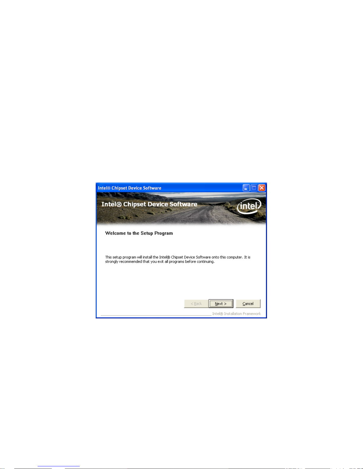
3.1 Intel Chipset Device Software
Step 1. Click “Next” to continue
Page 43
FEB-9455 User’s Manual
43
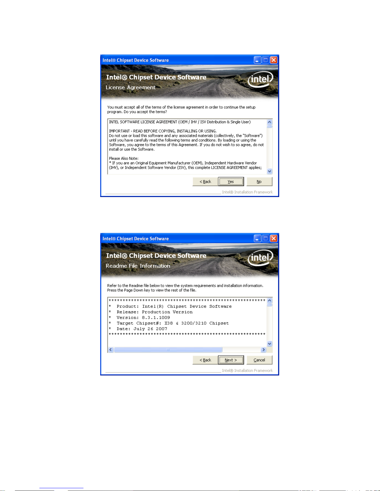
Step 2. Read the License Agreement and click “Yes” to continue
Step 3. Click “Next” to continue
Page 44
FEB-9455 User’s Manual
44
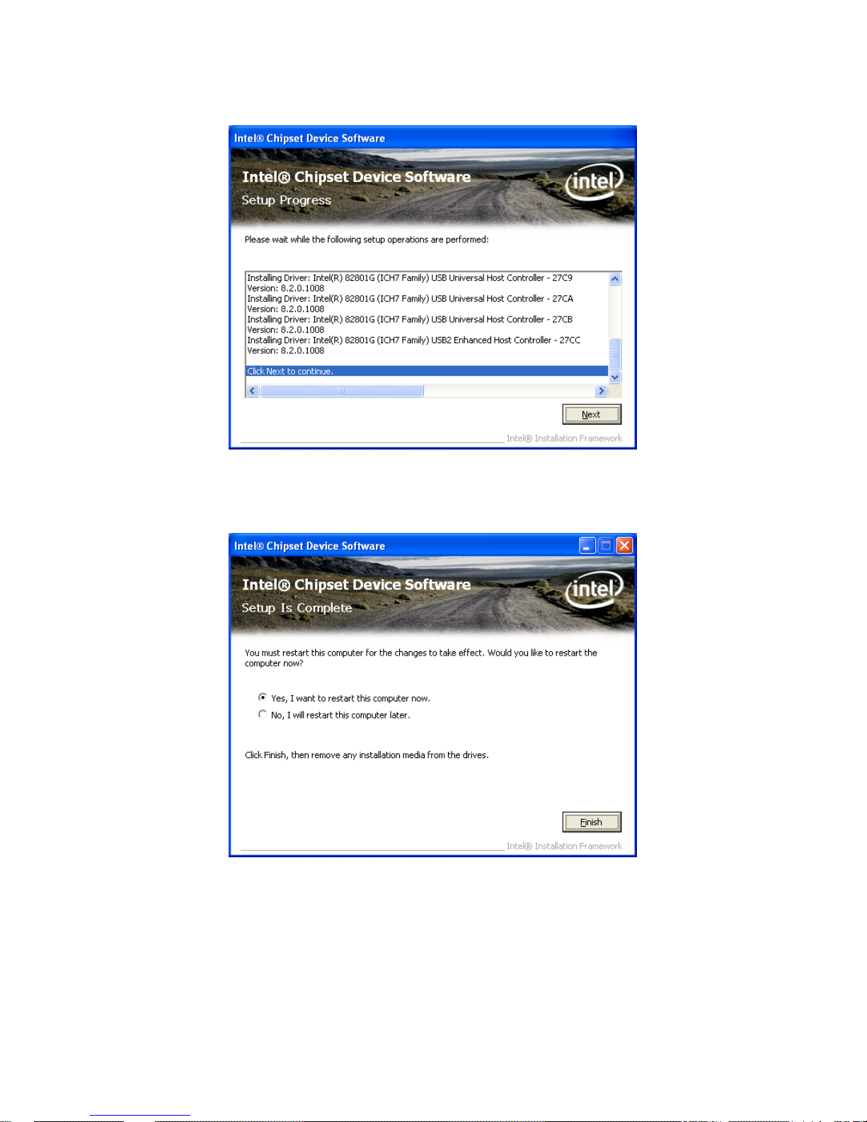
Step 4. Click “Next” to continue
Step 5. Click “Finish” to complete setup
Page 45
FEB-9455 User’s Manual
45
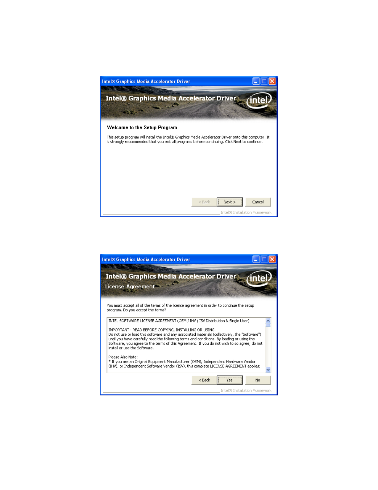
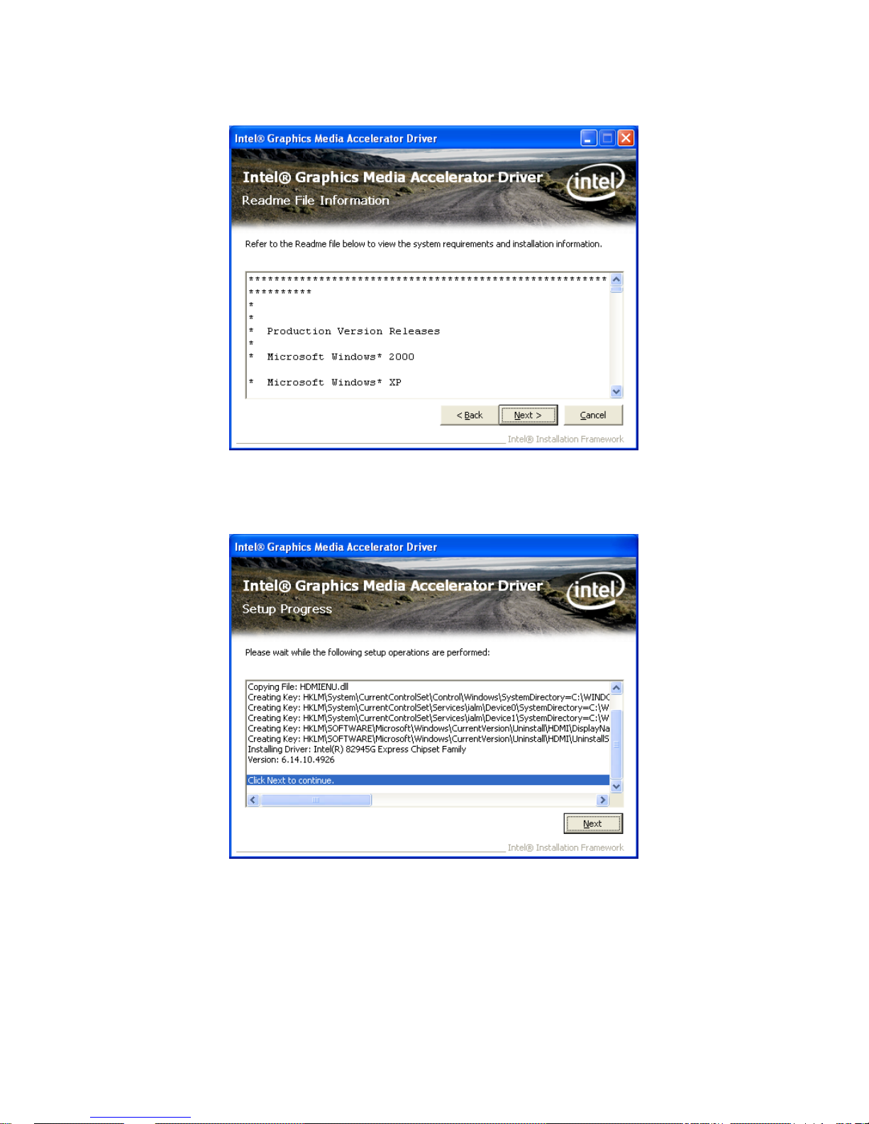
3.2 Intel Graphic Media Accelerator Driver
Step 1. Click “Next” to continue
Step 2. Read the License Agreement and click “Yes” to continue
Page 46
FEB-9455 User’s Manual
46
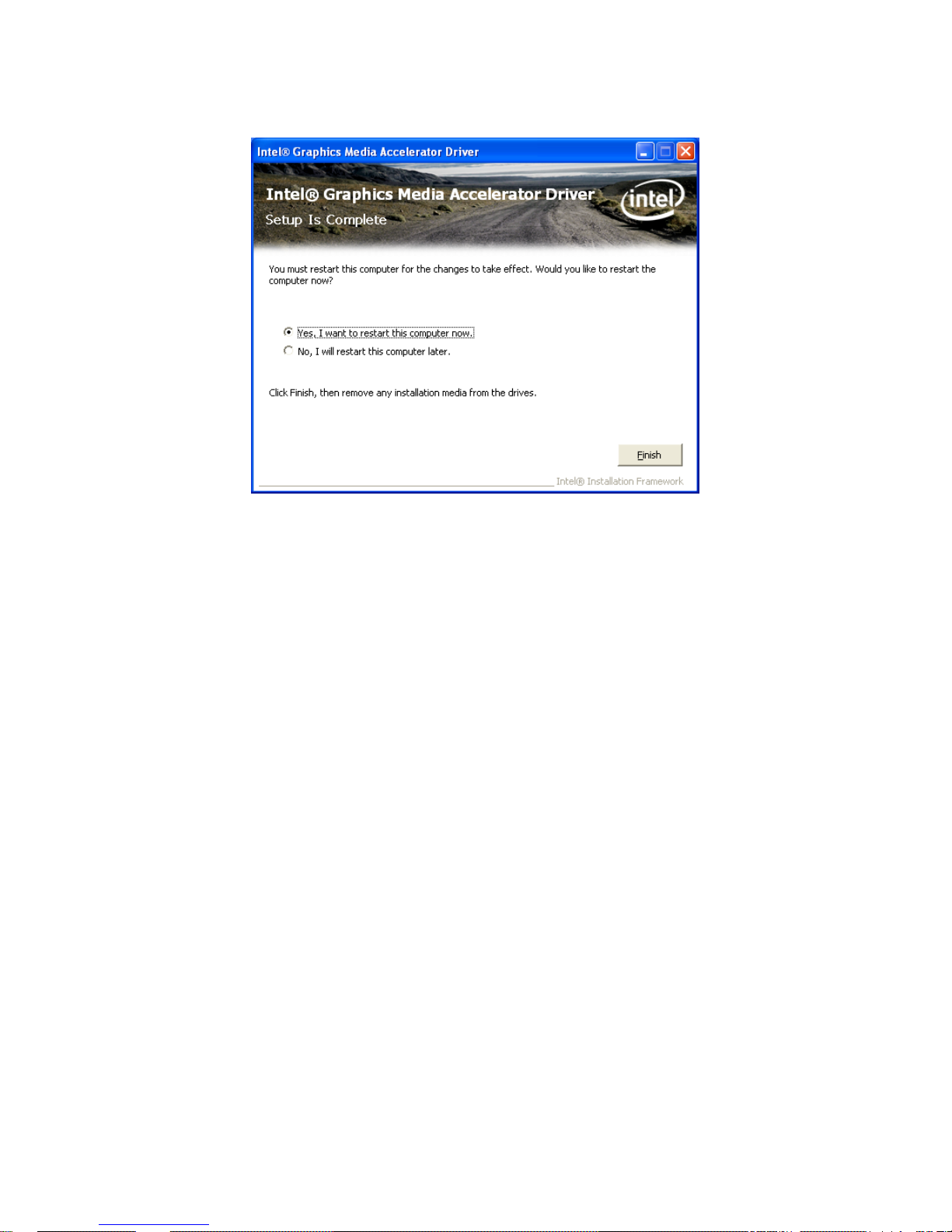
Step 3. Click “Next” to continue
Step 4. Click “Next” to continue
Page 47
FEB-9455 User’s Manual
47
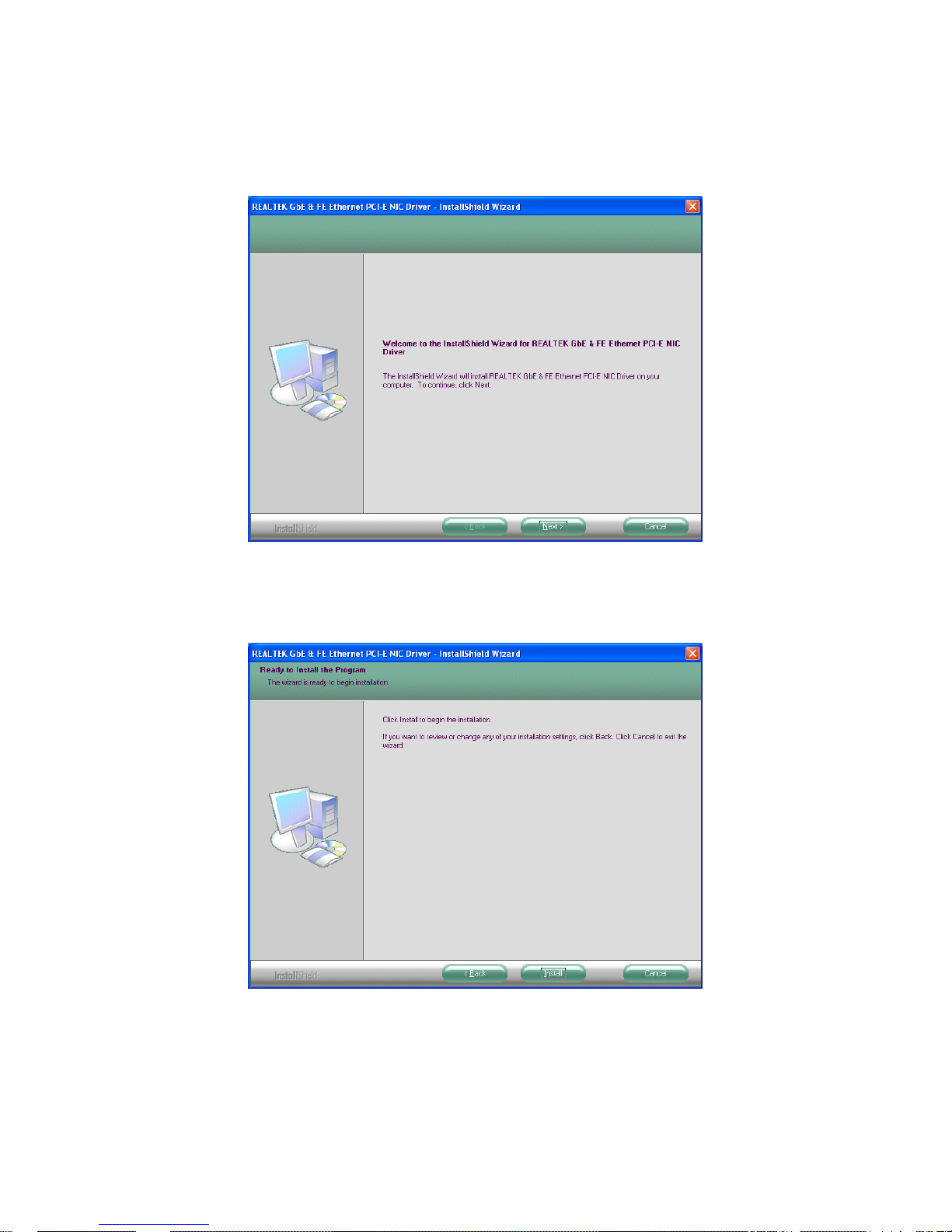
Step 5. Click “Finish” to complete setup
Page 48
FEB-9455 User’s Manual
48
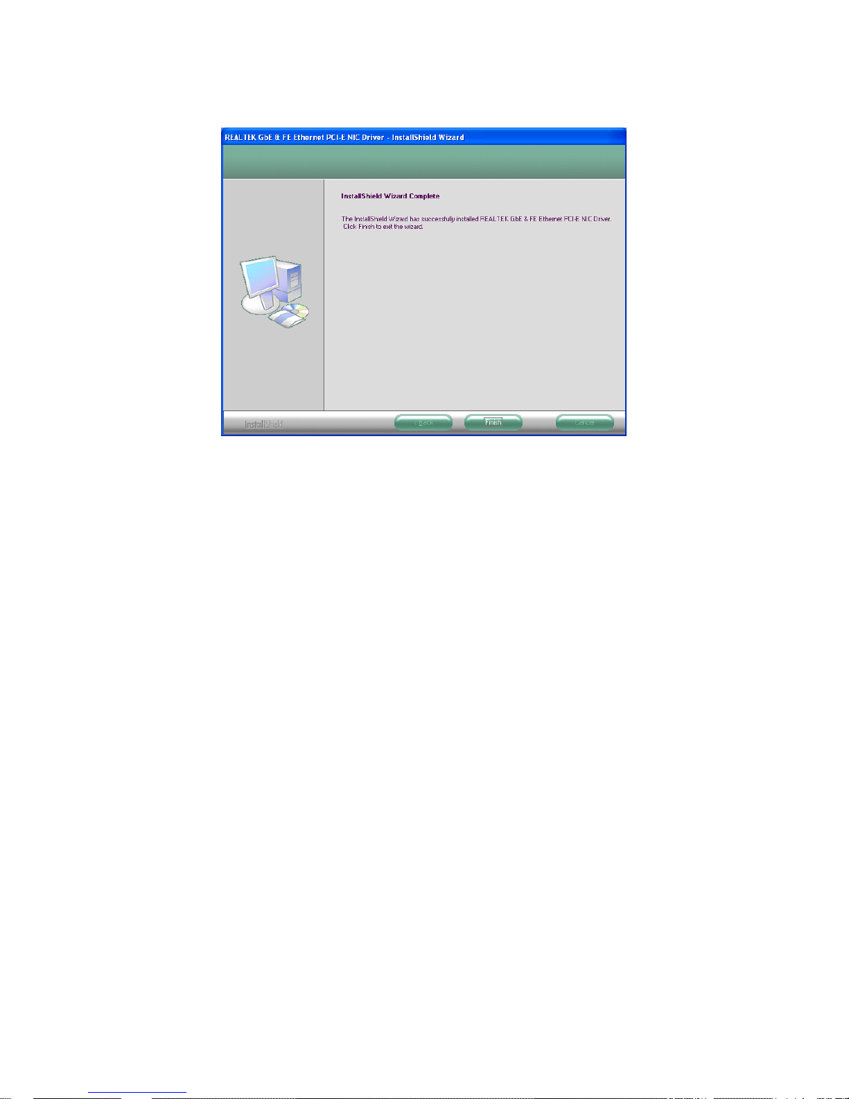
3.3 LAN Driver
Step 1. Click “Next” to continue
Step 2. Click “Install” to continue
Page 49
FEB-9455 User’s Manual
49
Step 3. Click “Finish” to complete setup
Page 50
FEB-9455 User’s Manual
50
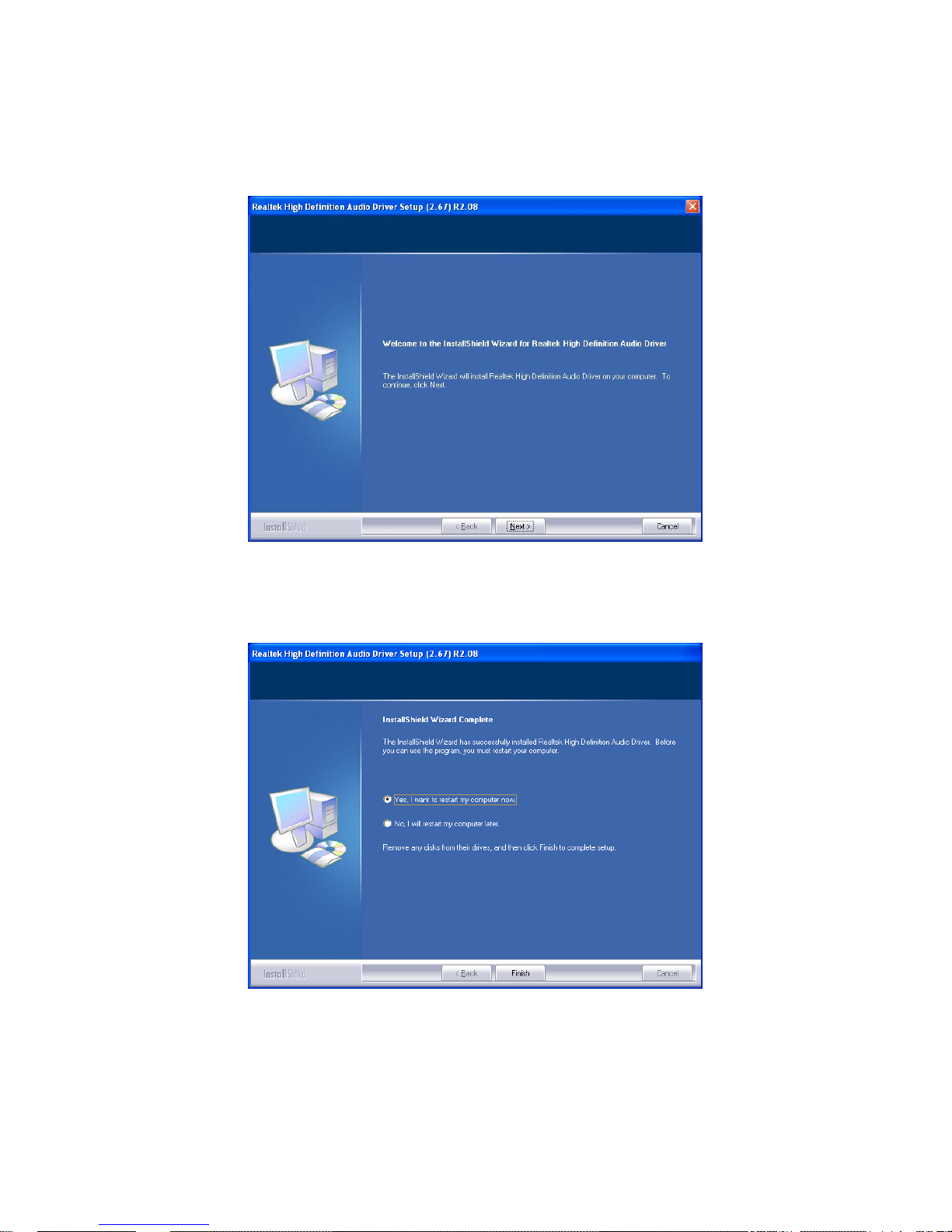
3.4 Audio Driver
Step 1. Click “Next”
Step 2. Click “Finish” to complete setup
Page 51

FEB-9455 User’s Manual
51
Appendix-A Watchdog
The system board provides Wat chd og function, the Super I/O setting step as below.
Step 1: CR2D, Bit0→0 (select pin77 to WDTO#)
Step 2: LD8, CR30, Bit0→1 (Active WDTO#)
Step 3: LD8, CRF7, Bit4→Write 0 to clear WDTO# status.
Step 4: LD8, CRF5, Bit3→0: Second mode, 1: Minute mode
Step 5: LD8, CRF6, Bit [7:0] →Set WDTO# Time out value. (WDTO# startup after
setting the system time, or setup from step 3 ~ step 5 to restart WDT.)
Appendix-B GPIO
The system board provides input and output ports that can be individually configured
to perform a simple basic I/O function. Users can configure each individual port to
become an input or output port by programming register bit of I/O se lection. To invert
port value, the sett ing of Inversion Regist er h as to b e made. Port values can be set to
read or write through Data Register.
Please refer previous chapter for pin define description.
Access Cash Drawer GPIO Programming Guide
There are two PNP I/O port addresses that can be used to configure GPIO ports,
(1). 0x2E - EFER (Extended Function Enable Register, for entering Extended
Function Mode)
- EFIR (Extended Function Index Register, for identifying CR index
number)
(2). 0x2F - EFDR (Extended Function Data Register, for accessing desired CR)
Below are some example codes for demonstrate GPIO function.
Page 52

FEB-9455 User’s Manual
52
// Enter Extended Function Mode
outp(0x002E, 0x87);
outp(0x002E, 0x87);
// Assign Pin121-128 to be GPIO port 1
outp(0x002E, 0x29);
outp(0x002F, inp(0x002F) | 0x01);
// Select Logic Device 7
outp(0x002E, 0x07);
outp(0x002F, 0x07);
// Active Logic Device 7
outp(0x002E, 0x30);
outp(0x002F, 0x01);
// Select Inversion Mode
outp(0x002E, 0xF2);
outp(0x002F, 0x83);
// Select I/O Mode
// Bit0~bit3 output and bit4~bit7 input
outp(0x002E, 0xF1);
outp(0x002F, 0x00);
// Access GPIO ports
outp(0x002E, 0xF0);
outp(0x002F, 0x7C);
// Exit Extended Function Mode
outp(0x002E, 0xAA);
Definitions of Variables:
Each bit in the lower nibble of each Register represents the setting of a GPIO port.
Bit0 vs. GPIO DIO-Out 0
Bit1 vs. GPIO DIO-Out 1
Bit7 vs. GPIO DIO-Out 3
Bit4 vs. GPIO DIO-In 0
Bit3 vs. GPIO DIO-In 3
Page 53

FEB-9455 User’s Manual
53
Value of Inversion Register:
Only lower nibble is available for this function.
When set to a ‘1’, the incoming/outgoing port value is inverted.
When set to a ‘0’, the incoming/outgoing port value is the same as in Data Register.
Value of I/O Selection Register:
Only lower nibble is available for this f unction.
When set to a ‘1’, respective GPIO port is programmed as an input port.
When set to a ‘0’, respective GPIO port is programmed as an output port.
Value of Output Data / Input Data:
Only lower nibble is available for this function.
If a port is assigned to be an output port, then its respective bit can be read/write.
If a port is assigned to be an input port, then its respective bit can be read only.
Note:
Some other functions may occupy the high nibble of the registers. Altering any
content in high nibble will be undesired.
 Loading...