

Page 1

FASTCAMERA USB
USER’S AND REFERENCE MANUAL
FVM-00398
1
Page 2

COPYRIGHT NOTICE
Copyright ? 2005 by FastVision LLC.
All rights reserved. This document, in whole or in part, may not be copied, photocopied,
reproduced, translated, or reduced to any other electronic medium or machine-readable
form without the express written consent of FastVision LLC.
FastVision makes no warranty for the use of its products, assumes no responsibility for
any error, which may appear in this document, and makes no commitment to update the
information contained herein. FastVision LLC. retains the right to make changes to this
manual at any time without notice.
Document Name: FastCamera USB User’s and Reference Manual
Document Number: FVM-00398
Revision History: 1.0 February 4, 2005
2.0 February 14, 2005
3.0 March 3, 2005
4.0 April 29, 2005
5.0 May 18, 2005
6.0 July 21, 2005
Trademarks:
FastVision? is a registered trademark of FastVision LLC.
Channel Link? is a trademark of National Semiconductor
Virtex? is a trademark of Xilinx Inc.
Windows?, Windows 95?, Windows 98?, Windows 2000?, Windows NT?, and
Windows XP? are trademarks of Microsoft
All trademarks are the property of their respective holders.
2
Page 3

FastVision LLC.
131 Daniel Webster Highway, #529
Nashua, NH 03060 USA
Telephone: 603-891-4317 Fax: 603-891-1881
Web Site: http://www.Fast-Vision.com
3
Page 4

Table Of Contents
COPYRIGHT NOTICE_____________________________________________2
USB2.0 USER’S GUIDE TO FC13 AND FC40 __________________________5
The USB 2.0 Versions of Fast Camera 13 and 40___________________________________________5
Computer System Requirements________________________________________________________5
Hardware and Software Installation_____________________________________________________6
Cables and Connectors ________________________________________________________________6
DirectX Installation___________________________________________________________________7
Installing Fast Viewer-USB Application__________________________________________________7
Using Camera for the First Time________________________________________________________7
FastCamera USB Operating Modes and States ____________________________________________8
Fast Camera-USB Application Controls_________________________________________________11
Continuous Capture and Preview Mode_________________________________________________________11
Setting Camera Capture Parameters____________________________________________________________ 13
Saving and Restoring Camera Settings _________________________________________________________19
Triggered Mode to Complete Capture of a Video Sequence _________________________________________ 19
Downloading Captured Video to the Host PC Mode _______________________________________________19
Review Captured Video in the Camera Memory __________________________________________________ 24
Specific Fast Camera Issues___________________________________________________________26
Trade-off between Frame Size and Frame Rate___________________________________________________26
Exposure_________________________________________________________________________________26
Triggering Video Recording Externally_________________________________________________________ 26
FastCamera Test Data _______________________________________________________________28
REFERENCE FOR THE FC13 AND FC40 CAMERAS___________________31
Control FPGA ______________________________________________________________________31
Sensor Control ____________________________________________________________________________31
Flash Memory ____________________________________________________________________________ 36
Serial Camera Control Interface_______________________________________________________________41
Inter-FPGA Communications_________________________________________________________________49
Embedded Soft Processor Core _______________________________________________________________ 50
Data FPGA_________________________________________________________________________59
DDR FPGA ______________________________________________________________________________59
Recording Modes __________________________________________________________________________59
Details of Implementation:___________________________________________________________________ 60
TROUBLESHOOTING ___________________________________________64
FASTVISION TECHNICAL SUPPORT_______________________________64
Contacting Technical Support _________________________________________________________64
Reporting Bugs _____________________________________________________________________66
4
Page 5

USB2.0 USER’S GUIDE TO FC13 AND FC40
THE USB 2.0 VERSIONS OF FAST CAMERA 13 AND 40
The USB 2.0 versions of Fast Cameras FV-13 and FV-40 make use of the widely used
USB 2.0 computer interface that can carry up to 40 MB/s of data. This interface is a
standard part of all recently manufactured desktop and portable computers. Since the
FastCamera image sensor is capable of capturing video data at rates higher than 660
MB/s such connection required re-thinking of the traditional digital video camera concept
and significant stand-alone operating capabilities in the camera itself.
The FastCamera-USB is able to capture digital video at a very high resolution and frame
rate and save it in the camera’s internal memory so it can be later downloaded directly to
the computer at the USB 2.0 data rate without the need for a specialized frame grabber
board.
COMPUTER SYSTEM REQUIREMENTS
Your computer must be running Windows 2000 or Windows XP for this software to work.
No other version will work, nor have they been tested.
You need at least 3GB of free space on the system’s hard disk to install the program, and
depending on the amount of memory in the camera, you may need more to store the
results. You need at least 256 MB of system memory.
You must have a USB 2.0 interface. The software will install but will not operate correctly
without one. In addition the software will not tell you, that you do not have the required
USB 2.0 interface. Please refer to your computer’s documentation to determine if you have
a USB 2.0 port. If you find you do have USB 2.0 support in your computer, you may have
to try all the USB ports to find the one that is actually USB 2.0, some of the older
computers did not have USB 2.0 on all of their USB ports.
The FastCamera USB will work with laptop computers that meet these requirements. Note
that some older laptop computers do not have USB 2.0 ports.
The FastViewer USB application will not interoperate with other USB cameras at the same
time. You must use the FastVision camera alone when you intend to use this software. It is
sufficient to un-plug your other USB cameras and you do not need to un-install their
software.
In addition only one FastVision USB camera will be recognized by the application software,
additional cameras will be ignored.
5
Page 6
DO NOT CONNECT THE U
SB CABLE TO THE
HARDWARE AND SOFTWARE INSTALLATION
Installation of the camera hardware is very simple and has only one hard rule:
CAMERA AND COMPUTER UNTIL THE
SOFTWARE HAS BEEN INSTALLED.
CABLES AND CONNECTORS
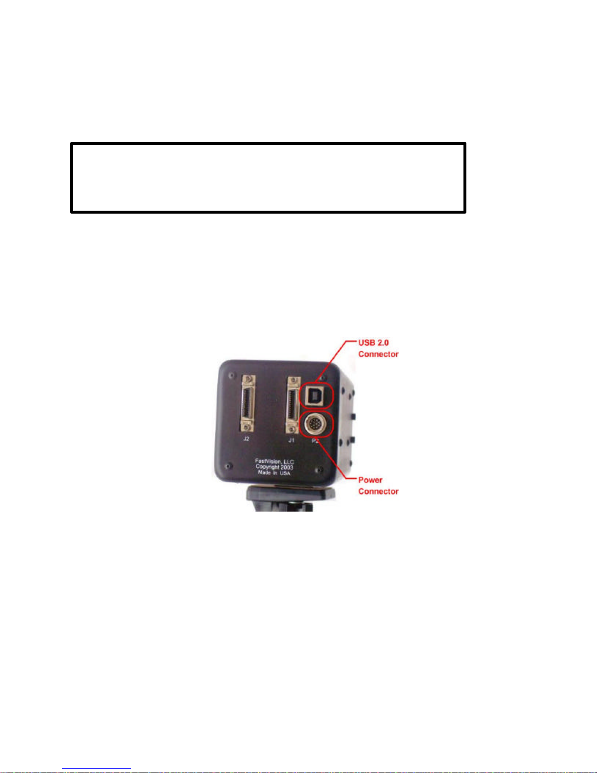
Operating the USB-connected FastCamera FV13 or FV40 require the use of only two
cables: Standard USB 2.0 AB cable and the Camera specific power cable that can be
optionally equipped with a connector for the external hardware trigger. The USB version of
the FastCamera uses only two connectors on the back of the camera. See Figure 1 below.
Figure 1. USB 2.0 and power connectors.
Connect the power supply cable to the camera first by gently rotating the round connector
until it finds the proper position and slides right in. Plugging in the power cable connector is
easy and doesn’t require any significant force. Disconnect the power cable by gently
pulling it out. No rotation is needed for disconnect.
After connecting the power cable to the camera, power it up by plugging one end of the
standard power cord in the power supply converter and the other end in the AC power
outlet. The LED on the converter box should display a steady green light. If this light is
blinking or dark, the power supply unit is damaged and must be replaced.
6
Page 7
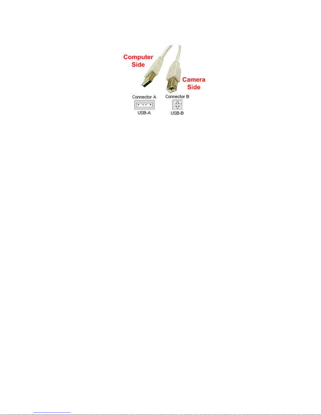
Figure 2. The USB 2.0 A-B cable
Connect the standard USB 2.0 AB computer cable to your computer but do not connect it
to the camera until after the FastCamera application software is installed.
DIRECTX INSTALLATION
Proper operation of the FastCamera USB requires presence of the up-to-date DirectX
support on the computer. There is a setup program for installation of Microsoft DirectX
version 9 on the Installation CD in a sub-directory called DirectX9. This software provides
many of the functions needed by the FastViewer application which may not be present on
your computer. The Microsoft installation program may require you to re-boot your
computer.
You should install DirectX support first, or at least before you run the FastViewer
application for the first time.
INSTALLING FAST VIEWER-USB APPLICATION
Run the setup.exe program on the root of the Installation CD. Take all the defaults but be
sure to read the Readme page (and the license page if you wish).
Just install and do not run the program initially. Start application only after you connect the
USB and power cables to the camera and follow plug-and-play hardware installation dialog
by taking all the defaults on the New-Hardware-Wizard. It is not necessary to try to find an
update on the Web. After the new hardware wizard tells you the hardware is installed, then
you can start the Fast Viewer-USB program.
USING CAMERA FOR THE FIRST TIME
When you start up the program you should see the main application screen like the image
in the Figure 3 below. You should see camera video in the rectangle. If you do not see
video, your camera may be powered off or it may not be generating images. Try pressing
the clear memory button to enable the camera video.
7
Page 8
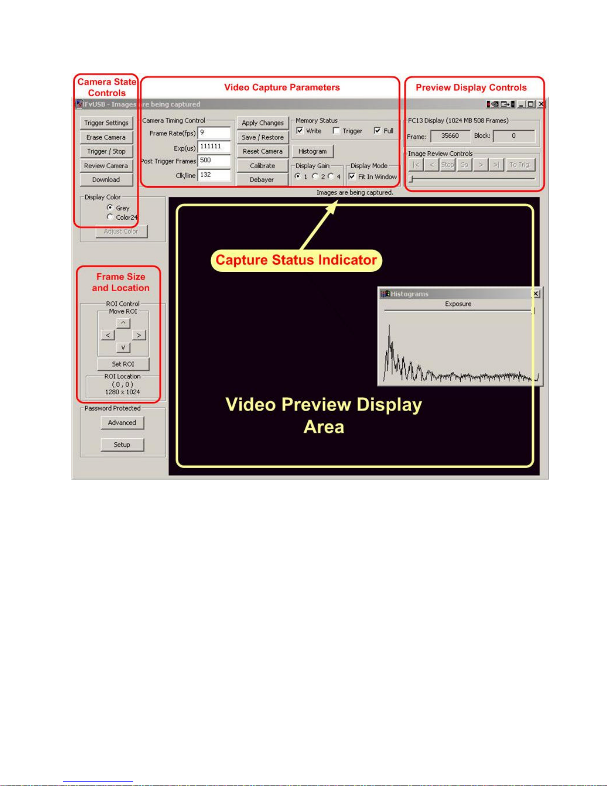
Figure 3. Fast Viewer-USB Main screen and camera controls.
FASTCAMERA USB OPERATING MODES AND STATES
Operation of the FastCamera USB is presumed to alternate between three main and one
optional state:
1. Continuous capture is the mode when all incoming video data are stored into the
circular buffer located in the camera memory. The preview images of the captured
video are down-sampled from their actual resolution to 640x480 pixels and
displayed in the Preview Display window. Erasing camera memory will restart this
mode from the beginning of the memory buffer. Asserting the internal or internal
Trigger will push the camera to switch out of this state and into the Triggered
8
Page 9

Capture state. Continuous capture mode is expected to be used as a main
maintenance mode to adjust camera parameters, target and focus the camera on
the object. You can end this mode only by asserting the internal or external Trigger
and shifting into the Capture Completion mode. The software version of the trigger
is asserted by clicking on the Trigger button.
2. The Trigger mode tells the camera to complete video capture into the internal
circular memory buffer by counting down the number of the post-trigger frames
specified by the operator. It starts by the assertion of the internal or external trigger
and stops at the last frame. At the completion of this task, the application
continuously re-displays the last captured image frame creating visual impression of
the stopped camera. Upon completion of the video capture sequence the camera’s
internal memory is full of video data that can be reviewed from that memory or
moved (downloaded) to the computer memory.
3. Downloading images from the camera’s internal memory buffer moves video data
into the host computer memory as TIFF files. Preview Video area is blank during
this operation. After completion of the download the camera retains all image data
until explicitly erased by the operator. The image download can be repeated
multiple times if necessary. The operator can observe the frame indicator and stop
download at any moment reducing the amount of storage used in the download
operation.
4. (Optional) –The operator can choose to review images stored in the camera’s
memory directly and decide if they should be downloaded or erased. This operation
requires download of only image headers to the host computer memory which is
usually faster than the full download. Most of the time this step is unnecessary and
images can be reviewed directly from the computer memory after the full download.
The diagram in the
Figure 4
below illustrates the camera operating modes and transitions
between them.
9
Page 10
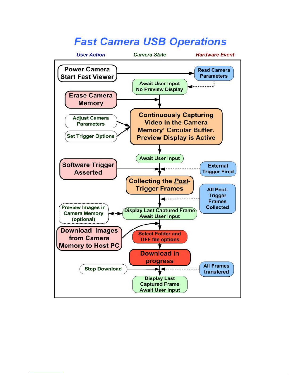
Figure 4, FastCamera Operating modes and transitions.
10
Page 11

FAST CAMERA-USB APPLICATION CONTROLS
The
Figure 3
camera mode.
Continuous Capture and Preview Mode
This is the main operating mode of the FastCamera. It is central to its operation and it has
the largest set of camera controls available for this mode. The FastCamera USB is forced
in the Continuous Capture and Preview mode by clicking the Erase Camera button. This
button starts every capture of the video sequence. It clears the camera memory, enables
new video capture to be written to camera memory, and starts the continuous video
capture in the circular memory buffer.
The visual indication of this mode is the live video display in the Video Preview area and a
checkmark appearing on the Write check box. It overwrites all video data you have
previously saved in the camera memory. The Write- box is checked when the camera is
writing to memory. During Continuous Capture mode the Download button is disabled.
(Getting images from memory while writing to memory is not supported).
Remember: every time the live video display stops after a trigger or a video download
operation just press the 'Erase Camera' button. This will again start the capture and the
live preview display albeit it will wipe out any image data you have recorded.
shows grouping of camera controls responsible for operation of each
The Full-Check box will be marked first time when the camera memory has been filled by
the incoming video data completely and image data collected earlier is being over-written
by new image data. The Full mark stays on until the camera memory is erased again.
You can not use the camera memory to store multiple recordings. The Erase Camera
button starts recording always at the beginning of the camera memory (address zero).
During the video capture the camera memory is treated as a ‘circular-buffer’. This means
that writing of images to memory begins at the start of memory and continues to the end of
memory and then wraps around to the beginning of memory again. Given enough time
older image data is overwritten with new image data. The number of images that the
camera can hold in memory can be computed from the following: a 1GB memory can hold
508, 1280x1024 images. If you set the frame rate to 500 frames per second this is just
about one second of video. (That is as fast as the camera can go at that frame size.) If you
take the ratio of the image size that has been set to the size of the full image and multiply
by 508 you can determine how many smaller images will fit. (508 *
1280*1024/(width*height) = number you can fit). If you have less than 1Gbyte in your
camera, scale the number again. When you download the images you can get the actual
number that fit.
11
Page 12

The ‘Reset’ button sends a reset command to the camera that restores its internal state
from the camera internal flash memory. This is the state you find the camera in every time
you power it up. You may want to force it if you find the camera is not operating after your
parameter changes as you expect it to or at all. You will need to Erase Camera after
Reset to re-start the live video preview.
The ‘Cal’ (Calibrate) button executes a self-calibration of the camera image sensor by
forcing an input offset null operation on the A to D converters behind each column in the
image sensor. This may improve image quality in some conditions. The typical indication to
perform that self-calibration is appearance of the bright vertical stripes in the image.
The Continuous Capture mode underlines most of the user interactions by providing the
live Video Preview display. The visual feedback is a necessary background for adjustment
of the camera video capture parameters to match requirements of the specific camera
application.
The Video Preview display area (open rectangle in the picture above), shows live video
from the camera so you can adjust camera capture parameters and point it at the object
you are going to image. Your first step is to communicate what kind of image sensor your
have in the camera: monochrome or color (Bayer filter). Click Grey or Color24 radio
button to reflect your choice. That selection affects only the Video Preview display.
Captured images will be stored on disk with the intact Bayer color filter information. A
special post-processing procedure, Debayer should be run to reconstitute precise color
information in the downloaded video images from the pixel values filtered by the Bayer
pattern in the color version of the camera.
Display of the Color24 images in the Video Preview window can be changed by clicking
on the Adjust Color button that will be activated by the Color24 selection. Again, that
adjustment affects only the Video Preview display.
12
Page 13
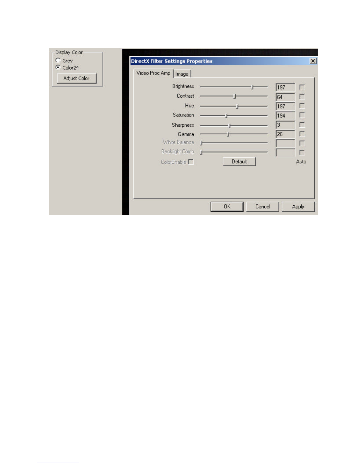
Figure 5, Color24 adjustment controls for the Video Preview display.
In some cases when the Visual Preview image is too dark or too bright to observe you
can do a quick image adjustment using the Display-Digital Gain control.
The Display-Digital Gain only affects the preview window images. If it is set to x1 then
you are looking at the upper 8 bits of the ten bit pixel (9:2), if it is set to x2 you are looking
at the middle 8 bits of the ten bit pixel (8:1), and if it is set to x4 you are looking at the lower
eight bits (7:0). The image data is not clipped or saturated, so you may see a kind of
striping artifact which is normal. It will not affect captured images in any way.
Setting Camera Capture Parameters
During Continuous Capture mode the operator is expected to verify correctness of the
camera setup and its targeting by looking at the Preview Display window. If necessary,
these parameters can be changed or adjusted.
The camera parameters can be grouped as:
? Image size and position in frame
? Frame rate and exposure
13
Page 14
? The type and relative position of the Trigger in the captured video sequence.
IMAGE SIZE AND POSITION
By default the FastCamera is set to capture video with the full resolution of the image
sensor in the camera. For various reasons that include increased capture speed and
number of image frames that can be stored in the camera internal memory, you may
choose to limit capture to a Region-Of-Interest (ROI) smaller than the full image frame. To
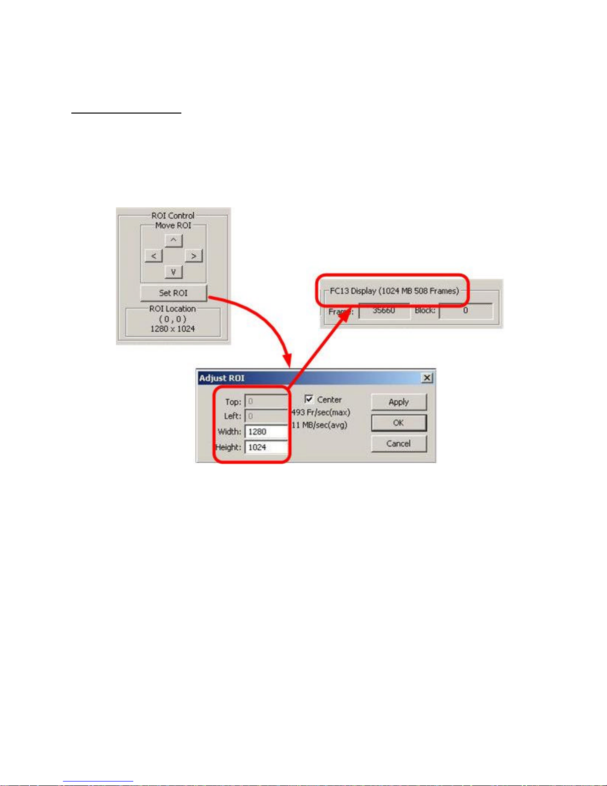
change ROI click on the Set ROI button to the left on the Video Preview Display area...
Figure 6, Changing ROI of the video capture
The 'Adjust ROI' combo box selects the height and width of the image to be recorded to
memory. The allowed widths go in steps of 10 pixels. The 'Height' combo box selects
the number of lines in the image. Make your change and click on the ‘Apply’ button. The
new image size will be sent to the camera and also reflected in the display at the upper
right corner that shows the camera inner memory size and how many frames will fit in.
If ‘Center’ check box is marked the application will compute the nearest offsets and
position ROI approximately at the center of the field of view. The new position will be
reflected in the grayed-out fields ‘Top’ and ‘Left’ for the upper left corner of the ROI. To
change these fields and place ROI somewhere else, uncheck the ‘Center’ box.
Occasionally, the ROI size is too big for the selected frame rate and should be brought in
compliance for the capture to work. You will be warned if the image height is too large for
14
Page 15
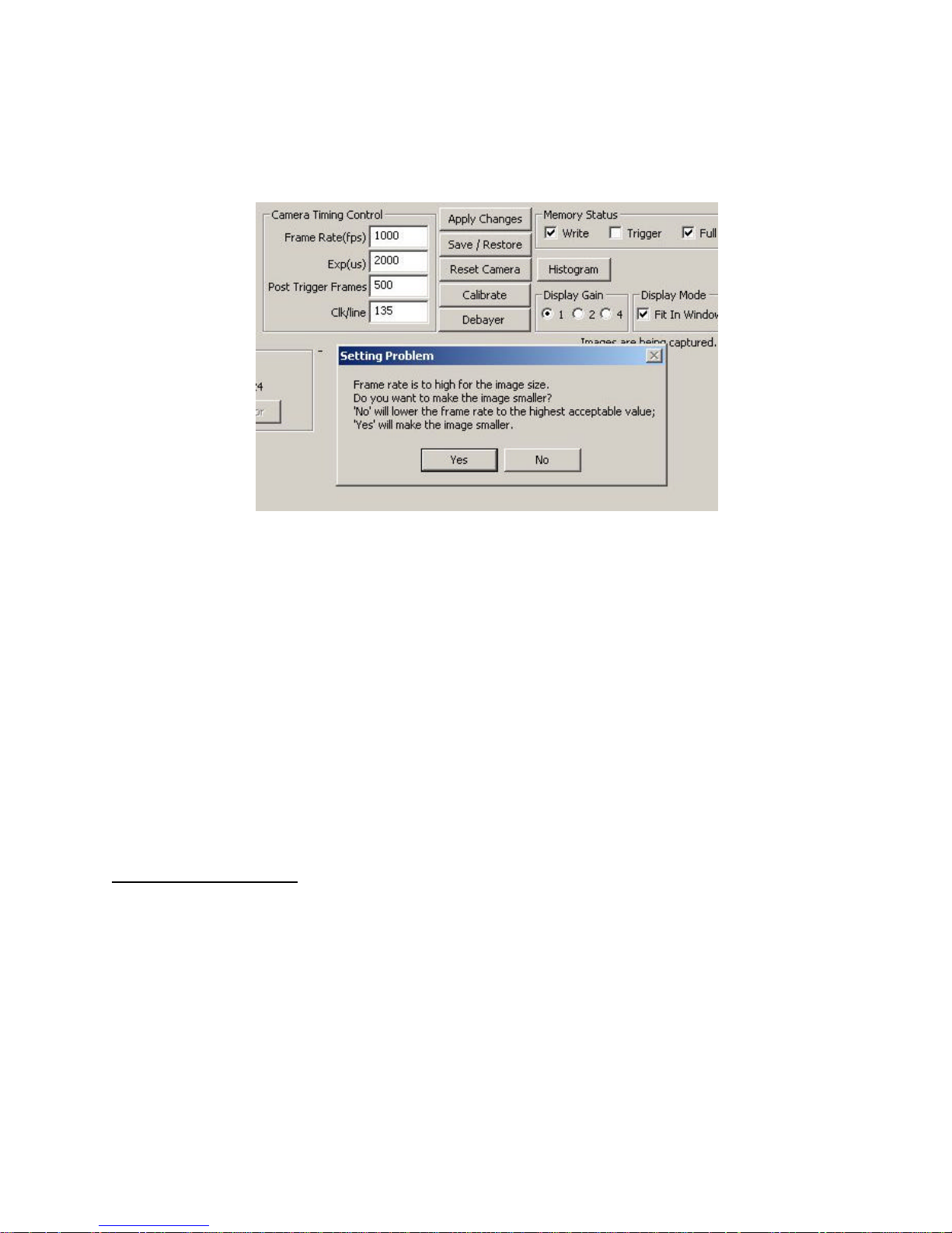
the frame period you have selected, after you press 'Apply-(Changes)' button. You will be
given a choice between a smaller ROI height and a lower frame rate. Applying your choice
the application will make the smallest possible change.
Figure 7, Changing ROI of the video capture
Any changes you make are not reflected in the camera until the Apply-Changes button is
pressed. The 'Apply' button collects the values of the various settings in the dialog,
verifies them, and updates the camera. If there is an error in your selected settings a
warning will pop-up and the offending value will not be sent to the camera.
The Preview Window is exactly 640x480 pixels. Selecting ROI sizes bigger than 640x480
pixels will only show you the upper left hand part of the image that fits in 640x480 preview
windows. (In fact the camera only sends the upper 640x480 pixels for that is all the USB
2.0 can support in real time.) The alternative to viewing only part of the ROI is to scale the
image down so it fits in the Preview Window. This is done by marking ‘Fit in Window’
check box. In that mode not every pixel in the ROI will be displayed. Downscaling preview
images with regular patterns can potentially create the fringe effect. It will not affect actual
captured images.
FRAME RATE AND EXPOSURE
You can type desired values for the Frame Rate and Exposure in their respective edit
boxes. The Frame Rate (fps) edit box allows the user to set the video capture frame rate
in frames per second. The Exp (us) edit box is used to define the exposure in
microseconds. Here is where you can change the exposure if you want it to be less than
the frame period. For obvious reasons, the exposure time can not be longer than the frame
rate. This limit is enforced by the program when you press the 'Apply' button. You will be
informed about this action and the new exposure value by the information window pop-up.
15
Page 16
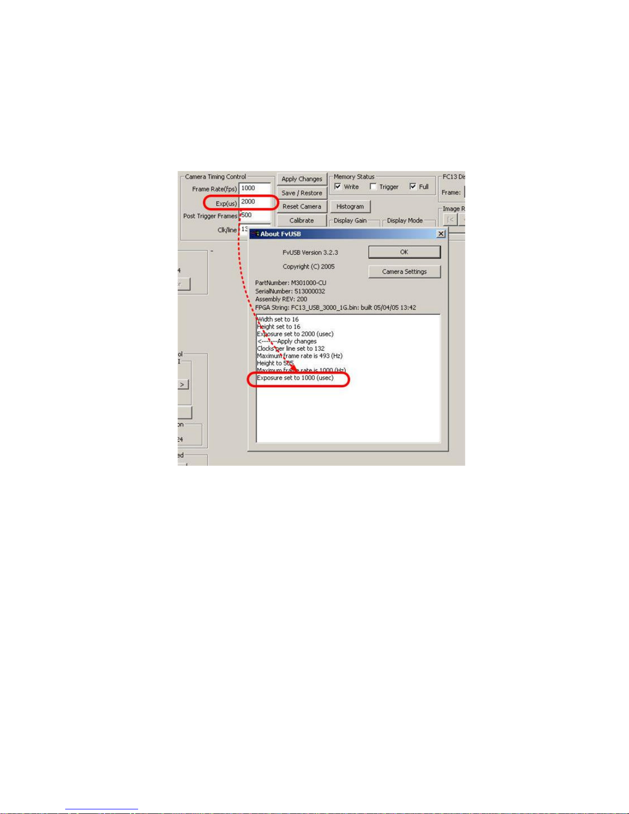
Figure 8, Adjusting exposure to the frame rate
The more intuitive method of setting and adjusting exposure is based on observation of the
Histogram or the preview video. The Histogram window insert is brought about by
clicking on the Histogram button above the Preview Window. It displays the frequency
plot of pixels values in the Preview Window with the lowest (darkest) values at the left side.
The Exposure slider control is placed directly above this plot. Changes in the exposure
will be immediately reflected in the image pixel values and in the changes to the Histogram
plot.
16
Page 17
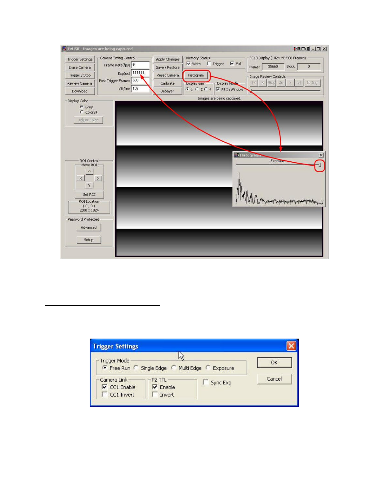
Figure 9, Using Image Histogram to adjust exposure
TRIGGER POSITION IN THE CAPTURE BUFFER
The 'Trigger-Settings' button brings up the Trigger Settings dialog which allows you to
choose and set the trigger mode of the camera.
See Figure 10 below
Figure 10, Trigger Settings dialog.
17
Page 18

The Trigger Settings dialog box controls the settings of the trigger in the camera.
Normally the camera should be in free-running mode, with P2 TTL Enable checked as in
the picture above. That configuration will support both, external and internal Trigger
modes.
The Camera link group box enables and controls the CC1 trigger input in the camera link
interface of the camera. Typically this is used in the configuration with a frame grabber
board and not with camera running in USB mode.
The P2 TTL trigger input is an input on an extra pin of the power connector of the camera.
If you have ordered a power supply with the trigger input option you will have a nine pin
connector where you can apply your trigger.
The Sync Exp check box should be left unchecked. It is documented in the detailed
documentation below and is typically not used
The FastCamera supports the following trigger modes:
Free Running in which the frame rate is determined by the value in the user interface.
Single Edge in which a frame is taken on each trigger from the digital input selected
below.
Multi Edge is not supported by the USB software, but provides for a burst of images to
be collected on each trigger.
The Post-Trigger Frames field defines the relative position of the Trigger in the captured
sequence of video frames. The Trigger can mark beginning, end, or somewhere in the
middle of the frames sequence depending on the user application. Its edit box takes a
number from zero to 65535, which is the number of frames to be taken before stopping
data collection after the trigger is detected (manual, through the software interface or
external, via a cable). Note: you can set the post trigger frame count so high that the
trigger image will not be in the camera memory’s circular buffer when writing stops; see the
discussion below about camera memory states. A value of zero will cause the camera to
stop immediately after receiving the Trigger.
Finally, the Clk/line field defines the number of clocks the camera uses to read out each
line from the image sensor. This should normally be set to 160 but can be as low as 135
clocks/line for the highest rate operation of the camera. It is normally used to slow down
the camera link output of the camera, which is irrelevant for USB operation of the camera.
This setting affects the maximum frame rate you can obtain with the camera. The frame
rate can not exceed the frame readout time which is equal to the Clk/line value plus 1
times the number of lines in the image divided by 66,666,666. (I.e. the sensor clock
speed). If you attempt to set the exposure to a larger value than the frame readout time
you will get a flashing effect with overall image brightness changing from frame to frame.
18
Page 19
Frame flashing is a sign that the exposure and frame rate are incompatible. Typically you
should set this to 160 and do not change.
Saving and Restoring Camera Settings
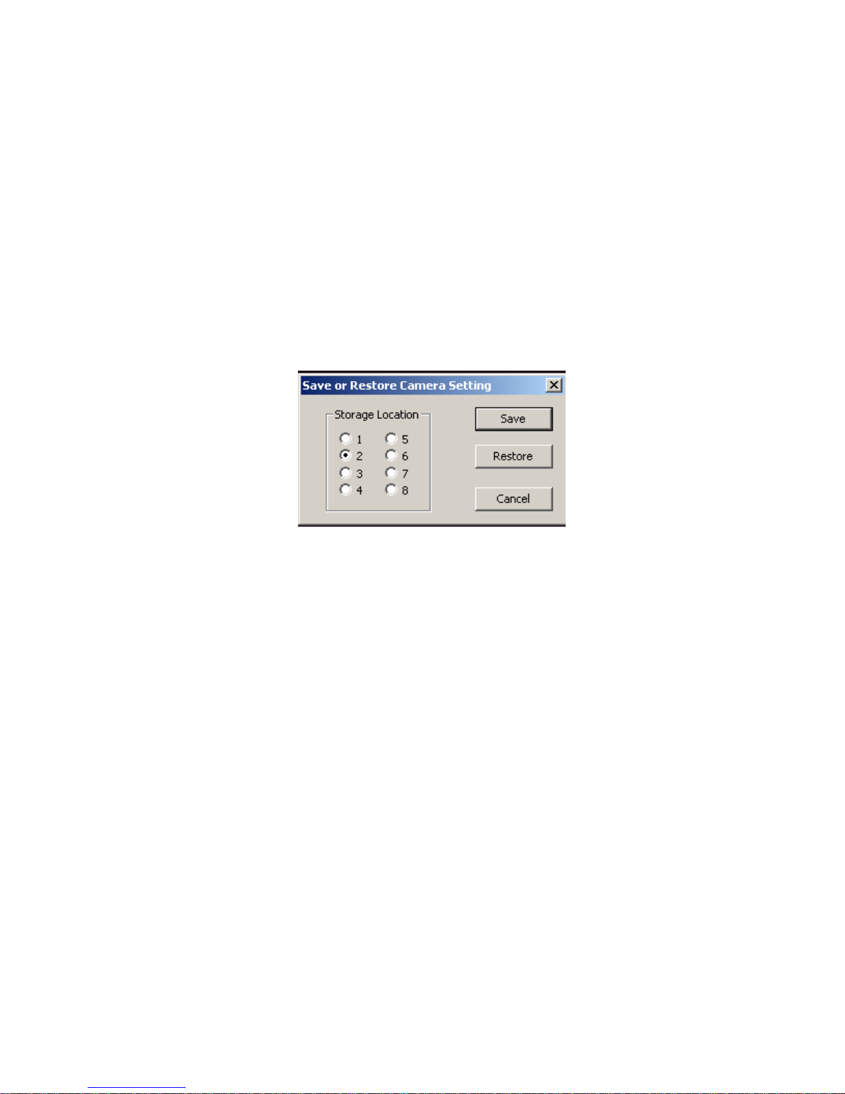
The internal flash memory of the FastCamera allows you to define the eight sets of the
camera parameters that can be saved and restored as needed. This is a great time saver if
you need to capture video with the same setup. Just click on the Save/Restore button and
you will see the dialog box as in the Figure 11 below. Select the desired parameter set
and click on the function button: Save or Restore. The first location has a special
meaning – the camera automatically loads the set 1 at the power boot-up. It is convenient
to keep your most often used settings stored in the first storage location. That will make
your settings immediately available on the power-up.
Figure 11, Saving and Restoring Camera Settings
Triggered Mode to Complete Capture of a Video Sequence
The 'Trigger' button sends the manual software trigger input to the camera. When the
camera is triggered by the internal or external event, it switches from the continuous video
capture mode to the video capture completion mode and begins recording post trigger
frames. When all the post trigger frames have been collected the camera stops and
continuously displays in the video preview window the last frame collected.
The Trigger-Check box at the top on the Main screen is marked when the trigger has been
detected by the camera. It is cleared when the camera memory is erased. The trigger can
come from either the software trigger button or an external hardware input signal (CC1 or
P2TTL).
Once this mode is triggered it will go to completion. The operator can’t interrupt it short of
calling the Windows Task manager and stopping the application.
Downloading Captured Video to the Host PC Mode
19
Page 20
The Download button initiates the process of getting the images sequence from the
camera memory to the host computer memory. It only works after the camera is triggered
and video capture to camera memory is stopped (see preceding explanation of camera
states).
The images from the camera’s internal memory buffer will be stored as TIFF files. Each
frame is stored as a separate file that receives a unique name derived from the internal
time stamp. (
Figure 12
below). The files are named:
YYYY_MM_DD_hh_mm_ss_INDX.tif or
YYYY_MM_DD_hh_mm_ss_INDX_trigger.tif .
Where YYYY is the year, MM is the month (01-12), DD the day (01-31), hh is the hour,
mm is the minute, ss is the second and INDX is the index of the image. The newest image
has index 0001 and will increase as the images get older. Note: the date and time reflects
the time that the image was written to the disk drive and not the time it was collected.
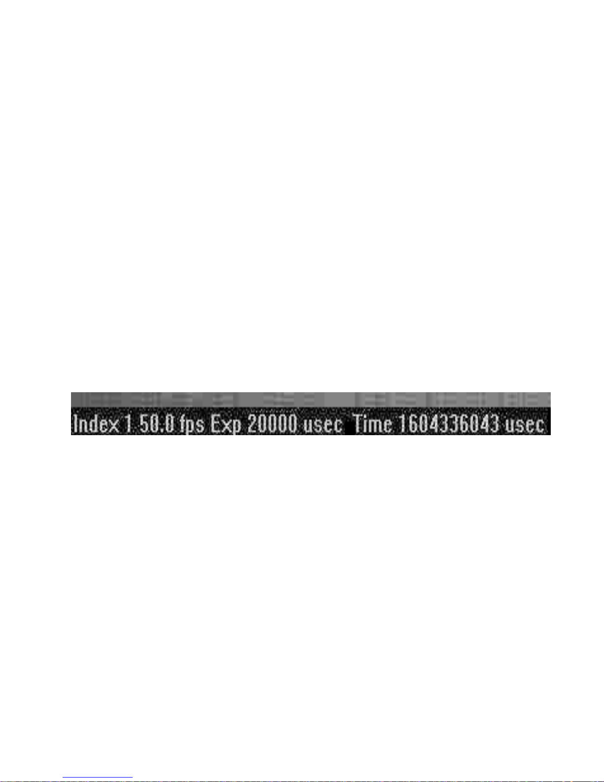
The essential video sequence information is also engraved at the bottom left corner of the
image. The time is a 32 bit quantity which is the number of microseconds since the camera
was turned on.
Figure 12, The frame sequence label
The filename for the frame captured at the trigger event has ‘trigger’ incorporated in the file
name to mark it.
Additional important information is also included in the tiff tags:
TIFFTAG_SOFTWARE = "FastViewer USB Application Version 3.0.1"
TIFFTAG_DOCUMENTNAME = the file name.
TIFFTAG_IMAGEDESCRIPTION = "Time Tick %d (usec)"
Application software can recover these values from the tags. In addition the files may be
renamed without loosing the original information in the names.
20
Page 21
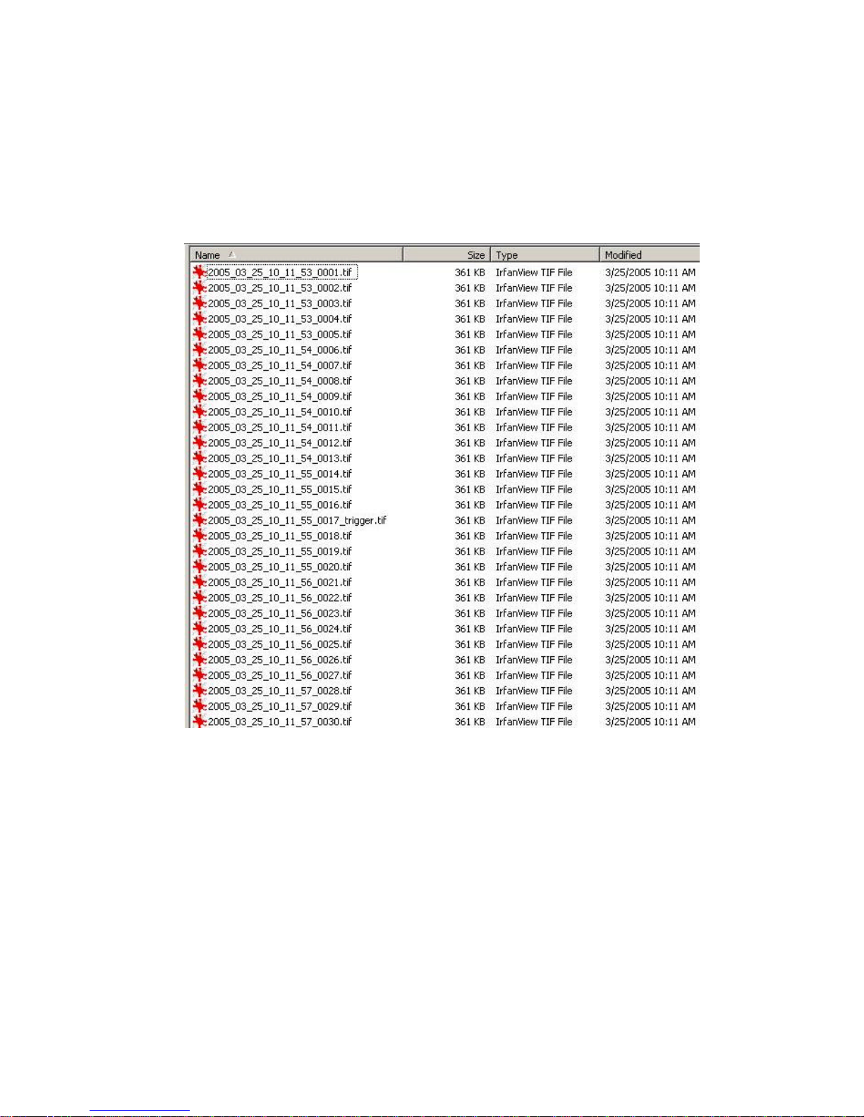
Figure 13, Video sequence list stored as TIFF files
The first step in this mode inquires operator about location to store camera images and
attributes of the TIFF files, as in the
Figures 14
21
and 15 below.
Page 22
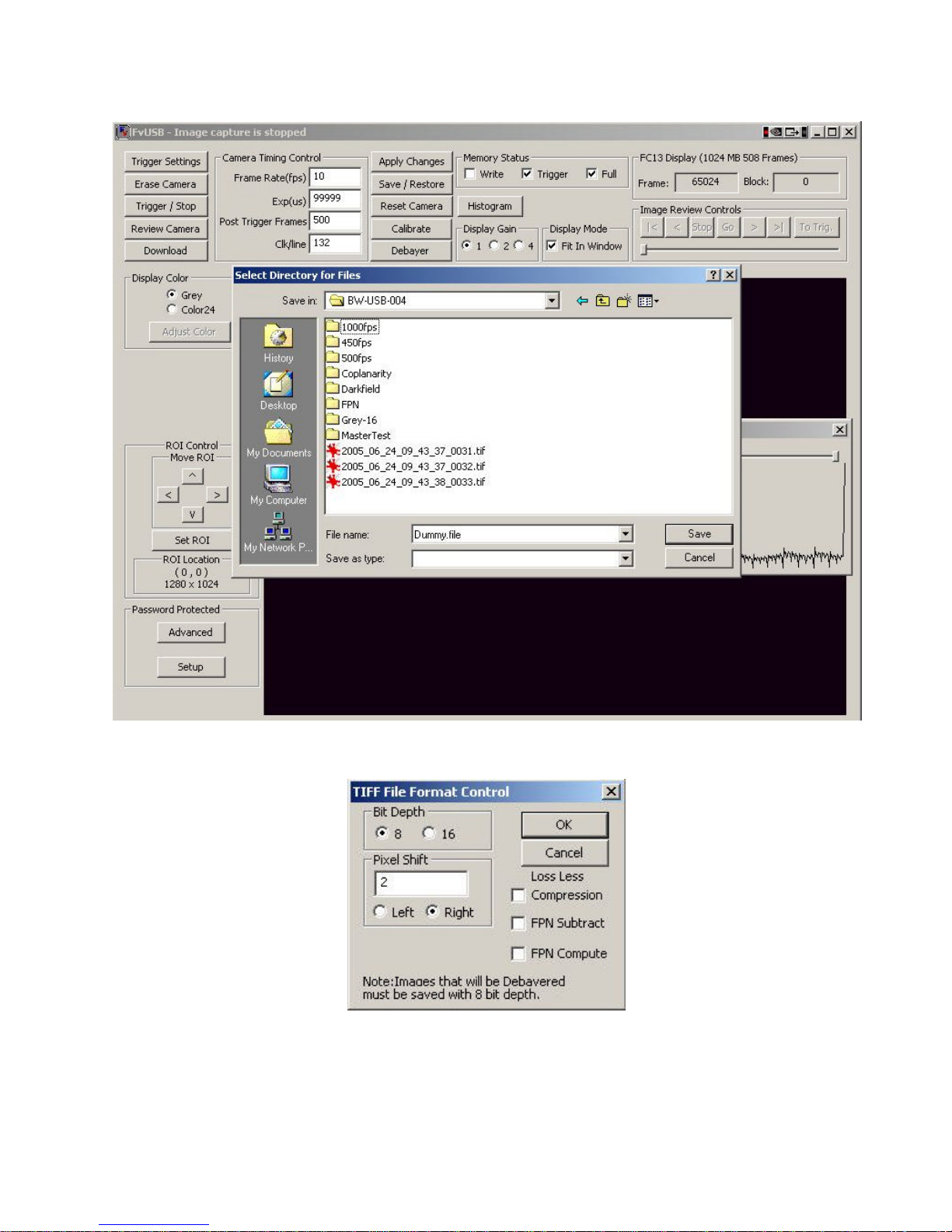
Figure 14, Selecting location to download images from the camera memory
Figure 15, Selecting image file properties and download type
22
Page 23

The image files can be recorded as the 8-bit or 16 bit TIFF files (8 or 16 bits per pixel) and
the pixel shift can be helpful in adjusting gain for the 8-bit files.
The 16-bit TIFF files can not be properly handled by many image viewer programs (notably
the one that is shipped by Microsoft with Windows). You could download the free image
viewer program, IrfanView from www.IrfanView.com; it can read and display the images
and their hidden TIFF flags. (Though it can not truly display the 16 bit pixels directly but
converts them to the 8-bit representation for display). Programs like Adobe Photoshop can
handle true16 bit images.
Selecting lossless image compression can halve the size of the image files and disk usage
but could complicate or prevent operation of many image processing programs.
The most important options during the image download refer to the image quality
enhancement by the removal of the fixed-pattern noise (FPN). The silicon area image
sensors by design are sensitive to micro-variations in the semiconductor manufacturing
process. These variations cause small differences in sensitivity of each pixel sensor.
Collecting images of these imperfections (FPN) and subtracting the FPN from captured
images will eliminate such variations. The FPN elimination helps especially with low-light
and low-contrast images that often occur with an insufficient lighting or too high capture
frame rate.
The FPN elimination is a two-stage process:
FPN Preparation
1. Set desired capture parameters.
2. Put lens cap on the lens to prevent light from getting in the camera.
3. Erase camera memory and trigger acquisition of the so-called “darkfield” images.
4. After capture stops, start image download in the directory where images will be
stored later and click on the FPN compute checkbox.
5. The camera will download 126 frames and will create an image file FPN_.....tif that
contains the FPN estimate.
FPN Image Use
1. Capture images as usual
2. Specify the same directory for the image download click on the FPN Subtract
button.
3. If the application doesn’t remember you doing the FPN preparation, it will ask you
to select an appropriate FPN file, like in the Figure 16 below.
23
Page 24
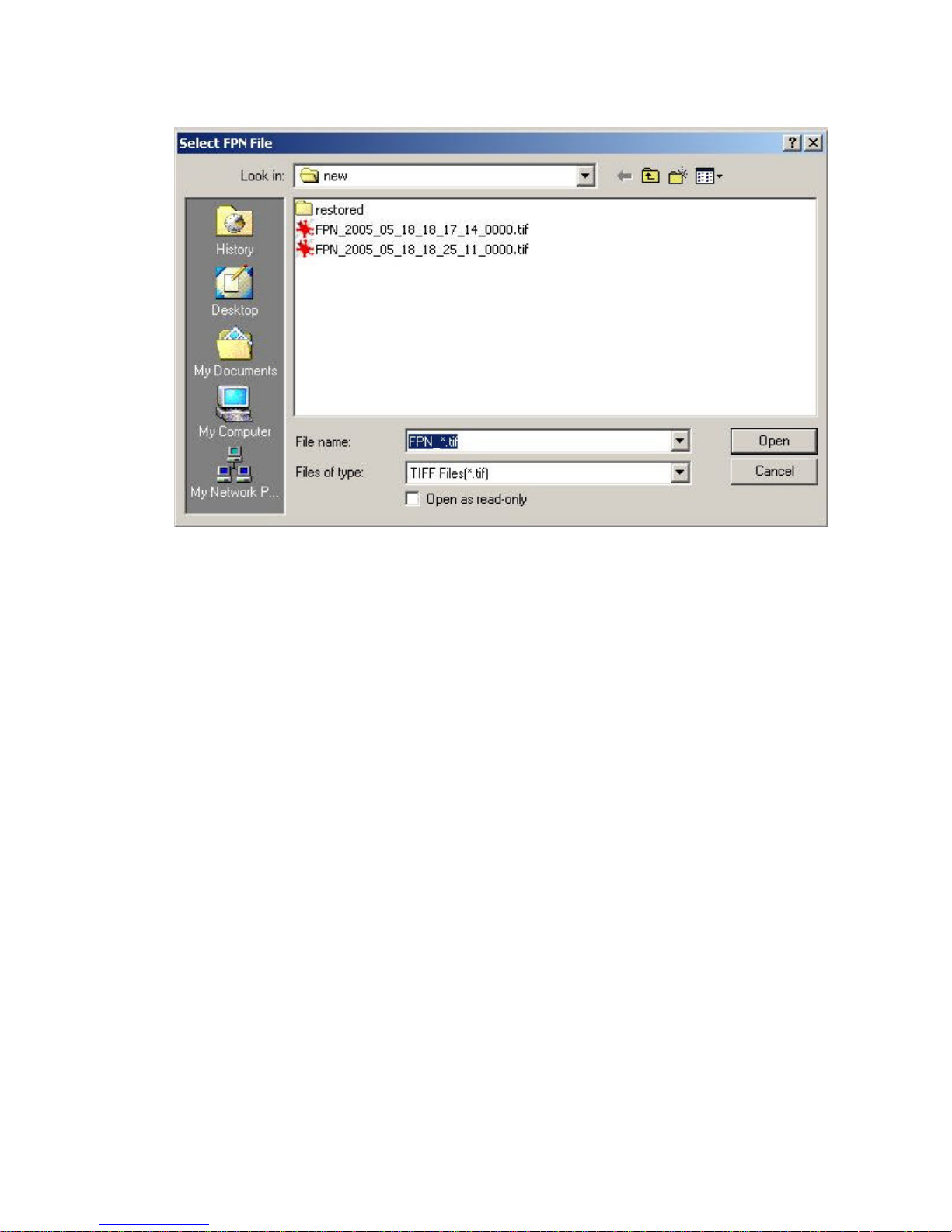
Figure 16, The FPN file selection
Two read-only indicators in the upper right corner of the window are very useful during the
image download:
The 'Frame' field indicates the frame number being read back.
The 'Block' field indicates the memory block number being read back (only useful to
programmers).
The image download process can be stopped by the camera operator by clicking on the
Stop Download button. That button appears in place of the Download button and stays
on during the image download process. The operator can time stop the action by use of
the Frame number indicator that displays how many frames were downloaded already.
Clicking on the Stop Download button brings up the Cancel Download dialog box and
the downloads stops only after confirming this action.
After downloading the images captured by the color version of the FastCamera the
operator can elect to convert images from the Bayer filter format to the RGB color. To do
this the operator clicks on the Debayer button and points to a directory holding previously
downloaded images captured by the color camera. The application creates a Restored
subdirectory and saves reconstructed color images in that subdirectory.
Review Captured Video in the Camera Memory
24
Page 25
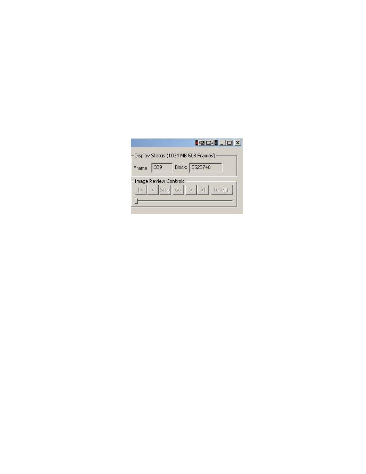
The Review Captured Video mode is only useable when the video sequence capture is
finished and the mark on the Write checkbox is off. When the Review Camera button is
pressed the FastViewer-USB application inquires the camera about the start of each
image in the camera memory. The Preview Display area is blank during this search since
the USB is carrying non-visual information. When this process is complete the images in
the memory can be previewed without actually transferring them all to the host computer.
The Review mode is able to show only 640x480 images. If the image size is set to larger
than 640x480 you will only see the upper left part of the image that fits in the 640x480
window or a decimated version that fits in the window. (This is limited by the USB 2.0
interface we are using).
Figure 17, The Review Captured Video controls
The Display-Digital Gain can be used again to enhance the preview window images. If it
is set to x1 then you are looking at the upper 8 bits of the ten bit pixel (9:2), if it is set to x2
you are looking at the middle 8 bits of the ten bit pixel (8:1), and if it is set to x4 you are
looking at the lower eight bits (7:0). The image data is not clipped or saturated, so you may
again see a kind of striping effect, which is normal.
The 'Go' button will begin displaying images from the current image pointer. The direction
is initially forward in time, but the '<' and '>' buttons can change this direction.
The 'Stop' button will stop the automatic display of the next image in sequence. The slider
and the '<' and '>' buttons can be used to step the display.
The button marked '|<' will move the image pointer to the first (earliest) image in camera
memory. The one marked '>|' will move to the last image in camera memory. The button
marked '<' will step to the previous image AND set the play direction to backwards. The
button marked '>' will step to the next image AND set the play direction to forwards. The
play speed is fixed by the performance of your computer and the USB interface, or 20
frames per second which ever is slower.
The 'To Trigger' button will position the image pointer on the trigger frame (i.e. first frame
acquired after the trigger assertion) and display it, if it is in the camera memory. If you set
25
Page 26

the number of post trigger frames to a large number the trigger frame may not be in
memory, and this button will not do anything except display a warning.
Remember: Review Captured Video mode can not be stopped until all header information
is collected from the camera memory. If you have a camera with a large memory and
have selected a small frame size it may take some time to find all the image headers.
A 1GByte camera can hold about 508 full size images (1280x1024) in memory. The
smaller your image the more will fit in memory. (640x512 images give you 4 times the
number or 2028 image). Note: the images are always stored in the camera memory at full
precision of 10 bits per pixel.
SPECIFIC FAST CAMERA ISSUES
Trade-off between Frame Size and Frame Rate
The FastCamera USB can read image lines from the sensor at a maximum rate of 500,000
per second (FV13) or 345,000 lines per second (FV40). These line rates are determined
by the Clk/line parameter that can not be smaller than the image sensor specified limit.
The height of the image you select will determine the maximum frame rate that you can
read from the sensor and write to memory. For example if you select 1280x128 line image
you can record at about 4,000 frames per second.
Note: the width of the image does not affect the frame rate, though it does affect the
number of images that will fit in memory.
If you attempt to set the frame rate to a higher value than the frame readout time
(determined by the number of lines in the frame and the line reading speed, see discussion
above), you will still get only the maximum attainable frame rate and not what you asked
for. You can always review the timer ticks recorded in successive images or over the
whole sequence to verify the actual frame rate if you have any doubts.
Exposure
Exposure can not be longer than the frame period. (1,000,000 / frame rate given as FPS).
The shortest exposure is limited by the software to values the camera supports. You can
get down to 2 microseconds (FC13) or 2.5 microseconds (FC40). Just make sure your
object is bright enough to be visible with a short exposure.
Triggering Video Recording Externally
EXTERNAL TRIGGER CONNECTOR
26
Page 27

The optional version of the FastCamera power supply and trigger cable assembly has a
DB-9F connector which allows user connection of a TTL trigger input to the camera via the
Camera's 12-pin Hirose round power connector. The connections are as follows:
PIN FUNCTION
1 Ground.
2 Expose output. This is a TTL-level signal which goes high while the camera's
electronic shutter is “open”.
3 Trigger output. This is a TTL-level signal which goes high for about 1 microsecond
when the camera has accepted a trigger. If a delay period has been specified, this will go
high at the beginning of the delay period, thus it can be used as an advanced notification
of exposure.
4 Trigger input. This TTL-level input can be programmed to trigger the camera on its
rising or falling edge, or used active high or low to control exposure directly, depending on
the trigger mode. The input is not terminated in the camera, so it is recommended to add
a pull-up resistor to +5V at the DB-9F connector.
5 Ground.
6 +5V. This is not intended to supply current for external devices, but only to allow
termination resistors to be added as described for the Trigger input. Recommended pullup value is 470 Ohms.
7,8,9 Not Connected.
DB-9F
Mating Face View
5 4 3 2 1
9 8 7 6
Figure 18, External Trigger connector.
27
Page 28
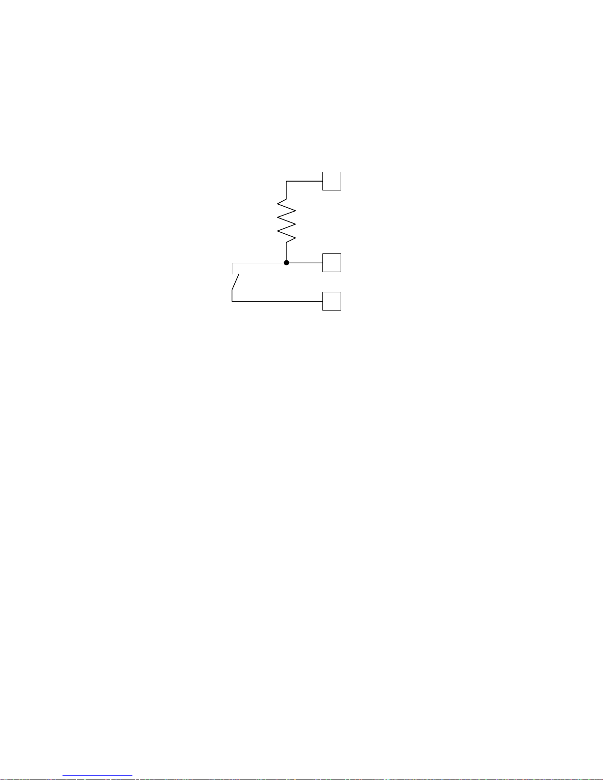
The input and outputs are 5V tolerant. Outputs have weak drive above 3.3V but may be
pulled up to 5V with an external 470 Ohm resistor. The trigger input is filtered in the
camera to remove glitches shorter that about 75 nanoseconds, however it is advisable to
provide a 1 microsecond minimum pulse-width for edge-triggered modes and 4
microsecond minimum for the direct exposure mode.
6
470 Ohms
4
5
Figure 19, Typical circuit for a switch contact trigger
FAST CAMERA TEST DATA
Each FastCamera is a precise and complex imaging instrument. It undergoes the thorough
outgoing testing with collected sample image data stored on the Test Data CD. This data
collected in a controlled and fully documented procedure can help customers in the
development of a sensor- and application-specific image corrections and enhancements.
The raw test data also serve as the baseline comparison in monitoring image sensor and
camera performance over time.
For the obvious reasons the test procedure and collected data set are somewhat different
for the color and monochrome image sensors. In both cases the test data is stored in the
raw, uncorrected format as the TIFF files. The raw tests data are accompanied by the
corresponding capture camera parameters.
The tests are identical for the FV13 and the FV40 FastCameras with some camera
parameters set at the different values for the high-speed tests.
The tests for the high frame rate uses a special bright LED counter test fixture that is set at
the 100 or 1,000 counts/sec. True camera frame rate is calculated from observations of the
counter transitions in the video sequence. The LED counter transition time and its
brightness are determined by the dwell time limits, its applicability to the measurement of
highest frame rates achievable by the FastCamera.
28
Page 29
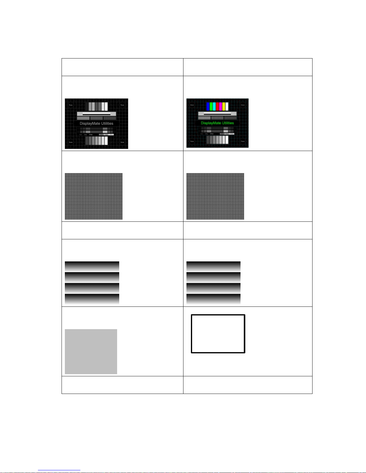
Monochrome Sensor Color Sensor
Master Test
Master Test
Co-planarity Test
Co-planarity Test
Darkfield Darkfield
Graywedge-16
Graywedge-16
Grayfield
Gretag Macbeth DC
White Balance
29
Page 30
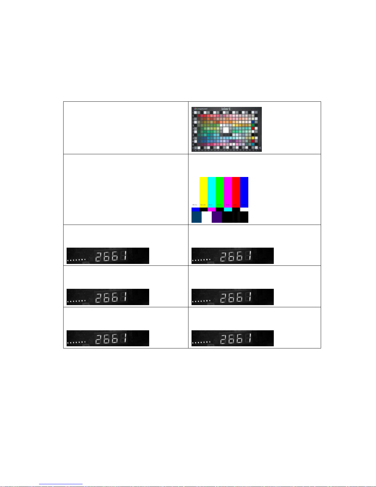
SMPTE
130 fps
450 fps
500 fps
130 fps
450 fps
500 fps
Figure 20, Fast Camera Test Suite
30
Page 31

REFERENCE FOR THE FC13 AND FC40 CAMERAS
The FC13 and FC40 cameras are based on a three FPGA design, a Control FPGA which
controls the timing of the sensor, a Data FPGA which handles specialized Data processing
functions and communication of results via USB or camera link, and a DDR FPGA which
controls the memory functions of the camera. In the USB version of the camera data flows
from the sensor to the data FPGA, then on to the DDR FPGA. From the DDR FPGA the
readout (preview and upload) takes data from memory and passes it back to the host. (The
writing and readout are asynchronous).
There are two separate sections in the DDR FPGA which provide the functionality of the
camera, the writer and the reader.
CONTROL FPGA
The following sections describe the Control FPGA in the FC13 and the FC40. It contains
an overview of functionality and some design details. Essentially the same design is used
on the FC13 and the FC40 cameras.
Sensor Control
LINE TIMING
Sensor line and frame rates are controlled by the Camera State settings. The minimum
line period depends on the sensor type and the ROI width. When the Line Period setting
exceeds the minimum period, extra clocks are inserted between lines. The Line Valid
period only depends on the ROI width and sensor type. The number of columns read from
the sensor is always a multiple of 10 for the MV13 and 16 for the MV40 sensor. Since the
Data FPGA also has access to the ROI settings it is possible for the actual ROI width (as
sent to the frame grabber) to start and end on any pixel, however this is not implemented.
The Control FPGA ensures that the starting and ending pixels of the ROI are read from the
sensor. For the MV13 this means as many as 9 pixels before and 9 pixels after the ROI
could be read from the sensor, depending on the starting and stopping pixel values modulo
10. For the MV40 sensor as many as 15 pre- and post-ROI pixels could be read from the
sensor, depending on the starting and stopping pixel values modulo 16. The software GUI
is responsible for determining the actual number of pixels per line based on the sensor and
readout mode.
Camera-Link or USB readout rate can be the limiting factor for the line rate in non-memory
modes. In this case it is the GUI's responsibility to maintain the Line Period setting large
enough to prevent FIFO overrun in the Data FPGA.
FRAME TIMING
31
Page 32
In free-running mode the minimum frame period depends on the ROI height and the line
period. When either the frame period or exposure time setting exceeds the minimum
period, extra clocks are inserted between frames. A 32-bit frame time counter allows
frame periods from the minimum up to 64 seconds in increments of 15 nsec.
In triggered modes the frame period is also affected by the exposure delay. In multiple
trigger mode the exposure delay only affects the time until the first readout of the trigger
sequence and subsequent frames run at the free-running rate as specified. In singletrigger mode with external exposure control, applying the trigger faster than the maximum
rate will cause the camera to skip triggers and run at a sub-multiple of the trigger
frequency. In multiple trigger mode and internal timed trigger mode, applying the trigger
faster than the maximum rate will result in the camera running at the specified free-run
rate.
Trigger pipelining is provided so that a trigger event which occurs during exposure or
readout (just during readout in external exposure mode) will generate another frame.
FRAME SIGNALS TO DATA FPGA
Line Valid and Frame Valid are sent to the Data FPGA and Memory FPGA on the
fpga_ctl2 and fpga_ctl1 signals respectively. The assertion edge of Frame Valid always
leads Line Valid by at least one sysclk cycle. Frame Valid also serially transmits status
after the leading edge of Line Valid for the first line of each frame. The Data and Memory
FPGAs filter this out to create Frame Valid internally. The first status bit is valid one clock
cycle after the rising edge of Line Valid on the first line. Bit order of the status signals is:
Trigger Event (1 bit indicating external trigger since previous frame).
Frame Number (32-bit number as returned by H command) MSB first.
Frame Timestamp (32-bit number in microseconds) MSB first.
The Frame Timestamp is taken at the end of exposure, which may or may not have a
constant time relation to the time of readout. The 32-bit counter free-runs starting at 0 at
power up and wrapping every 71 minutes 35 seconds (approximately).
EXPOSURE MODES
The MV13 sensor is normally used in TrueSNAP shutter mode. The sensor has analog
frame storage and a transfer gate that allows exposure to overlap readout while exposing
all lines together. The MV40 sensor does not have analog storage and can only be
exposed in a rolling shutter mode. Thus the individual lines have different exposure
windows which may or may not overlap depending on the line rate and exposure time
settings. This is the equivalent of using the MV13 sensor with the transfer gate on all the
time.
32
Page 33

When viewing high-speed motion, the MV40 works best if the lines are read out at the
maximum possible rate while additional time for exposure or frame period is inserted
between frames. This maximizes the overlap in the line exposure times. Unfortunately in
the non-memory readout modes with reduced output rates just the opposite must be done.
Long interline delays in these modes causes excessive temporal distortion in the moving
image. This can appear as stretching or shrinking of vertically moving objects or
trapezoidal distortion of horizontally moving objects.
TRIGGER MODES
There are four basic trigger modes:
Free-running mode ignores trigger inputs and reads out the sensor continuously at a
programmed frame rate with programmed exposure timing.
Multi-frame edge-triggered mode activates a programmed number of exposures after a
programmed delay at a programmed frame rate with programmed exposure timing.
Single edge-triggered mode activates a programmed exposure after a programmed delay.
External exposure mode exposes during the active trigger period.
Free-running mode allows continuous readout at rates ranging from about one frame per
minute to the maximum capability of the sensor. Exposure can be programmed in
increments of 15 nsec up to the frame period. There are gaps in the allowable exposure
times due to interaction between the readout circuitry and pixel reset in the MV13 sensor.
In the MV40 sensor the exposure time is even more restricted due to the rolling shutter
mode of operation. The Control FPGA will generate the exposure timing as close as
possible to the requested value.
Multi-frame edge-triggered mode effectively starts the camera into free-running mode for a
programmed number of frames after a delay of zero to about 64 seconds programmable in
15 nsec increments. The active edge of the trigger activates the time delay and the first
exposure starts after this delay. The camera can be re-triggered during active readout. If
re-trigger event occurs too soon to start the subsequent exposure after the programmed
delay, the next exposure will start as soon as possible thereafter. This prevents the effect
of running at submultiples of the trigger rate when the trigger rate exceeds the capability of
the camera.
Single edge-triggered mode is the same as asynchronous multi-frame edge-triggered
mode with the frame count set to 1.
External exposure mode starts exposure as soon as possible after the active-going edge
of the trigger and stops exposure as soon as possible after the inactive-going edge of the
trigger. For the MV13, this provides accurate exposure timing based on the trigger pulse
33
Page 34

width. For the MV40, limitations of the rolling shutter limit the exposure timing resolution to
the line readout rate unless the exposure time exceeds the readout time. Subsequent
exposures can overlap readout of the current frame in this mode. This can place further
restrictions on the exposure timing resolution in both sensor types.
The MV13 camera has "synchronous" and "asynchronous" modes of exposure. These
only apply to free-running and multi-frame modes. Single-frame and external modes are
always "asynchronous." When the synchronous trigger mode bit is set, the exposure
timing is linked to the readout timing to avoid exposure period jitter that can occur when
the readout overlaps the exposure. In multi-frame triggered mode, the synchronous mode
also creates an additional delay of one readout time that must be added to the
programmed delay to find the actual delay to the first exposure.
TRIGGER OPTIONS
There are four trigger sources - Camera Link CC1, TTL trigger input, Serial, and USB (via
I2C).
The CC1 and TTL sources can be enabled or disabled. They can also be active high
(positive-going edge for edge-triggering or high level for external exposure) or active low
(negative-going edge for edge-triggering or low level for external exposure).
The Serial source uses the "O" command. This cannot be disabled in the Control FPGA.
It must be disabled by the GUI if desired.
The USB source uses writes to sub address 0x63. In external exposure mode two writes
are required. Writes to sub address 0x63 with bit 0 high starts the exposure, and writes to
sub address 0x63 with bit 0 low ends the exposure. This cannot be disabled in the Control
FPGA. It must be disabled by the GUI if desired.
TRIGGER OUTPUTS
There are two trigger outputs, both TTL level on the P2 power connector. One output is
high whenever the sensor is exposing. The other is high during the programmed delay
period in the two edge-triggered modes.
REFERENCE VOLTAGES
All sensor reference voltages are programmable and generated by two LTC1660 octal D/A
converters. At power-up the DAC's are loaded with default values hard-coded into the
Control FPGA. After the Data FPGA has been loaded the DAC's are updated with the
settings in the default camera state storage page of flash memory.
34
Page 35

Comparators in the Control FPGA check for changes in the DAC settings and re-load the
DAC's whenever the values are changed. This can happen as a result of the host
command to set camera state, or the host command to restore state from flash.
CALIBRATION
Both the MV13 and MV40 sensors have automated ADC calibration to reduce column-wise
fixed-pattern noise. This is initiated at sensor reset or by using the CAL_START_N input.
The Control FPGA always uses the sensor reset to initiate calibration. In addition, the
MV40 sensor allows direct access to the internal calibration values on a serial interface
consisting of the DATA_CLK, DATA, RE_N, and WE_N pins. This version of the Control
FPGA does not use this interface.
Automatic calibration is initiated after power-up when the sensor is released from reset.
Reset is released before the Data FPGA is loaded to allow the sensor to stabilize during
the load process. Reset is re-asserted for two clock cycles at the end of the initialization
sequence, about TBD milliseconds after the reference voltage DAC's are updated from
flash. This causes the sensor to re-calibrate with the new reference voltage settings.
After power-on initialization, the sensor is only calibrated on demand by the host using the
Reset and Calibrate Sensor command. It is not automatically calibrated after changing the
reference voltages. Thus the camera control GUI is responsible for periodic calibration as
required.
POWER-ON INITIALIZATION
The Control FPGA has a small embedded micro that runs through an initialization
sequence at power-on. This same micro also implements the host, USB, and Data FPGA
communication protocols and deals with flash memory and DAC's.
Immediately after power-on, the voltage reference DAC's are programmed with factory
default values. This allows the sensor to stabilize under conditions close to the actual
operating environment.
Page zero is read from the flash memory. This page holds information necessary to locate
actual power-on data in the flash.
The sensor is released from reset and allowed to self calibrate and stabilize.
The Data FPGA is loaded from flash. If the offset or length stored in the header is not
valid, the embedded micro skips to step 10. This may take several seconds depending on
the FPGA size.
35
Page 36
Camera State is read from one of the 8 pages as selected by the pointer in the header. If
the pointer is not valid (1 - 8) or the selected page is uninitialized, the embedded micro
skips to step 10.
Reference DAC's are reprogrammed with the updated values from flash.
Camera State is forwarded to the Data FPGA.
If the Pointer to the Data FPGA initialization area is valid and the length is valid and non-
zero, the Data FPGA initialization is read from flash and forwarded to the Data FPGA.
The sensor is briefly reset to start another auto-calibration cycle.
The embedded micro enters the command service loop.
Flash Memory
Table 2 shows the layout of flash memory. The first page is used only for main header
information. Following this are eight pages for storing up to 8 camera states. FastVision
reserves one of these for factory defaults #1. Any of these states can be chosen as the
power-up default.
Flash Page Layout
Page Offset Pages Description
0 1 Flash Memory Header Page
1 1 Camera State Storage 1
2 1 Camera State Storage 2
3 1 Camera State Storage 3
4 1 Camera State Storage 4
5 1 Camera State Storage 5
6 1 Camera State Storage 6
36
Page 37
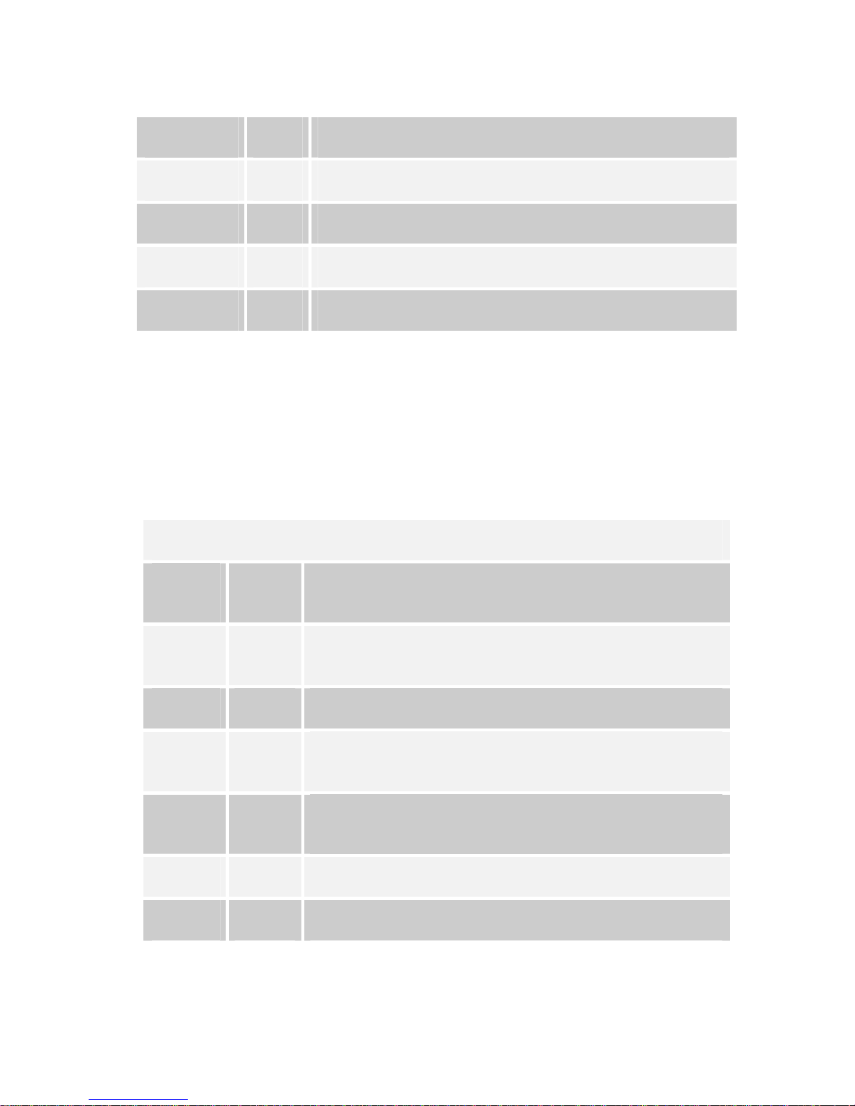
7 1 Camera State Storage 7
8 1 Camera State Storage 8
9 1370 FPGA bit stream (sized for 2V1000 + 2V250)
1379 2716 Available for Data FPGA Initialization and User Data
4095 1 Reserved
Table 2 - Flash Memory Layout
Table 3 shows the layout of the first page in flash memory. This contains enough
descriptors for the Camera Control GUI to determine the camera type and its options. This
data should only be programmed by FastVision. The camera GUI software must enforce
this, as there is no write protection built into the Control FPGA firmware. Multibyte values
are little endian.
Page Zero Flash Header
Byte
Offset
0 1
Bytes Description
Flash Memory Part Type: 0x16 or 0x32 for 16 or 32
Mb flash
1 1 Flash Memory Revision ID: 0x01 for this revision
2 2
4 4
Offset in bytes to Camera ID data from top of page
0: 0x79 0x01
Flash page offset to FPGA data: 0x09 0x00 0x00
0x00
8 4 FPGA bit stream length in bytes
12 4 Flash page offset of Data FPGA initialization data
37
Page 38
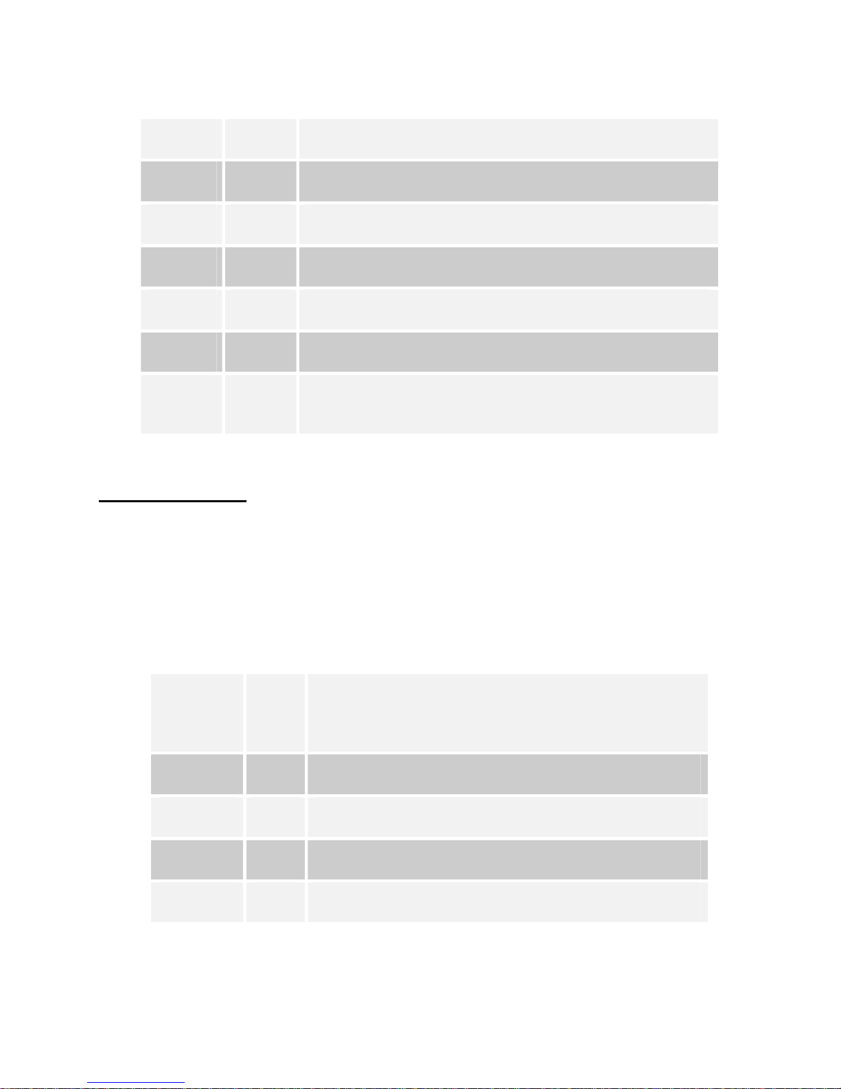
16 4 Data FPGA initialization data length in bytes
20 1 Camera State to load at power on (1 to 8)
20 357 Reserved for additional header / ID info
377 11 Part Number, ASCII "800??-5????"
388 3 Part Revision, ASCII "010"
391 9 Serial Number, ASCII "XXX??????"
400 128
FPGA bit stream file header from mkbin, Null
terminated string
Table 3 - Flash Memory Header Page
CAMERA STATE STORAGE
Internal to the Control FPGA all state is saved in a Block RAM. Copies of the current state
can be saved to the flash or uploaded to the host. The current state can also be retrieved
from flash or changed by the host. Only the host has random access to the camera state
and this only when setting state. Reading back the camera state always sends the entire
state to the host. Table 4 shows the layout of the camera state memory. Except for
sensor reference voltages, multibyte values are little endian.
Byte
Offset
Bytes Description
(decimal)
0 4 C3, 5A, F0, 69 for detecting uninitialized buffers
4 2 Vln2: 14 D9
6 2 Vref1: 14 D9
8 2 Vtest: 20 00
38
Page 39
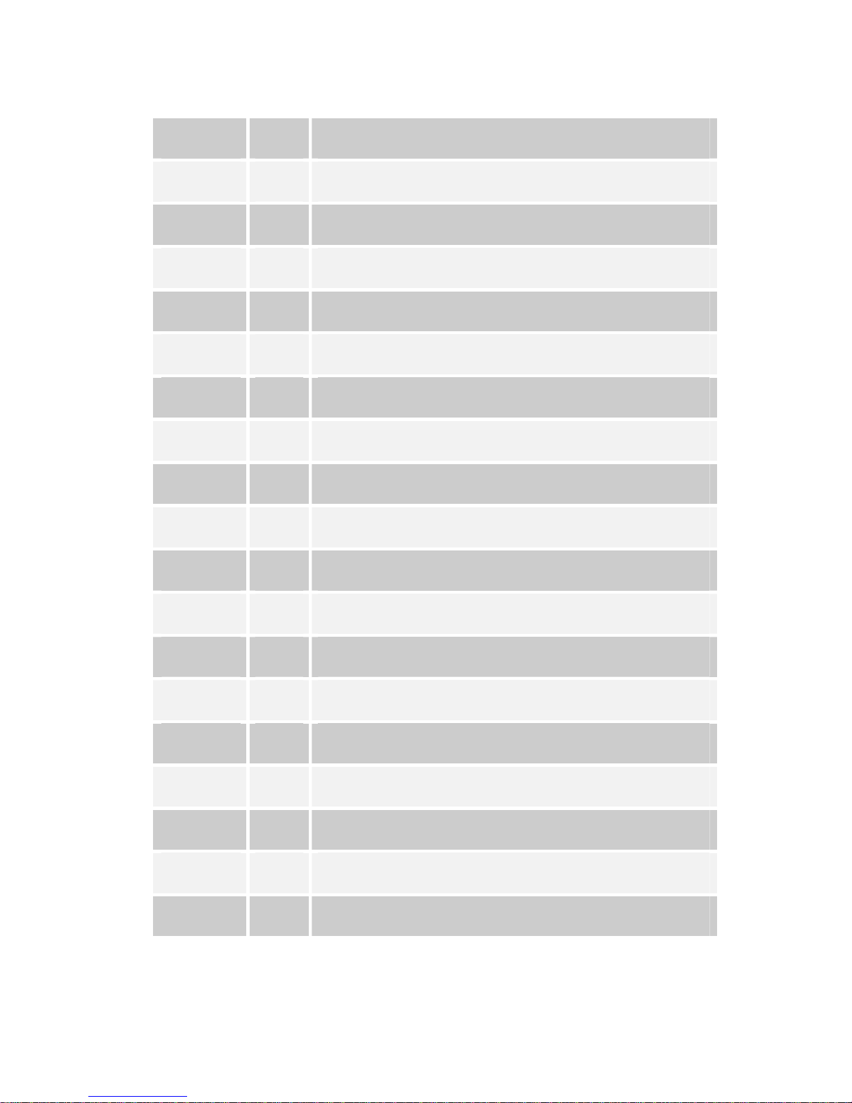
10 2 Vref2: 23 E0
12 2 Vbias1: 30 00
14 2 Vref3: 32 E8
16 2 Vbias2: 40 00
18 2 Vref4: 41 36
20 2 Vbias3: 50 00
22 2 Vln1: 54 D9
24 2 Vbias4: 60 00
26 2 Vlp: 64 D9
28 2 Vunused1: 70 00
30 2 Vclamp3: 70 00
32 2 Vunused2: 80 00
34 2 Vrstpix: 8D 17
36 2 ROI Start Pixel
38 2 ROI End Pixel
40 2 ROI Start Line
42 2 ROI End Line
44 2 Line Period in Pixel Clocks
46 4 Exposure Time in Pixel Clocks
39
Page 40
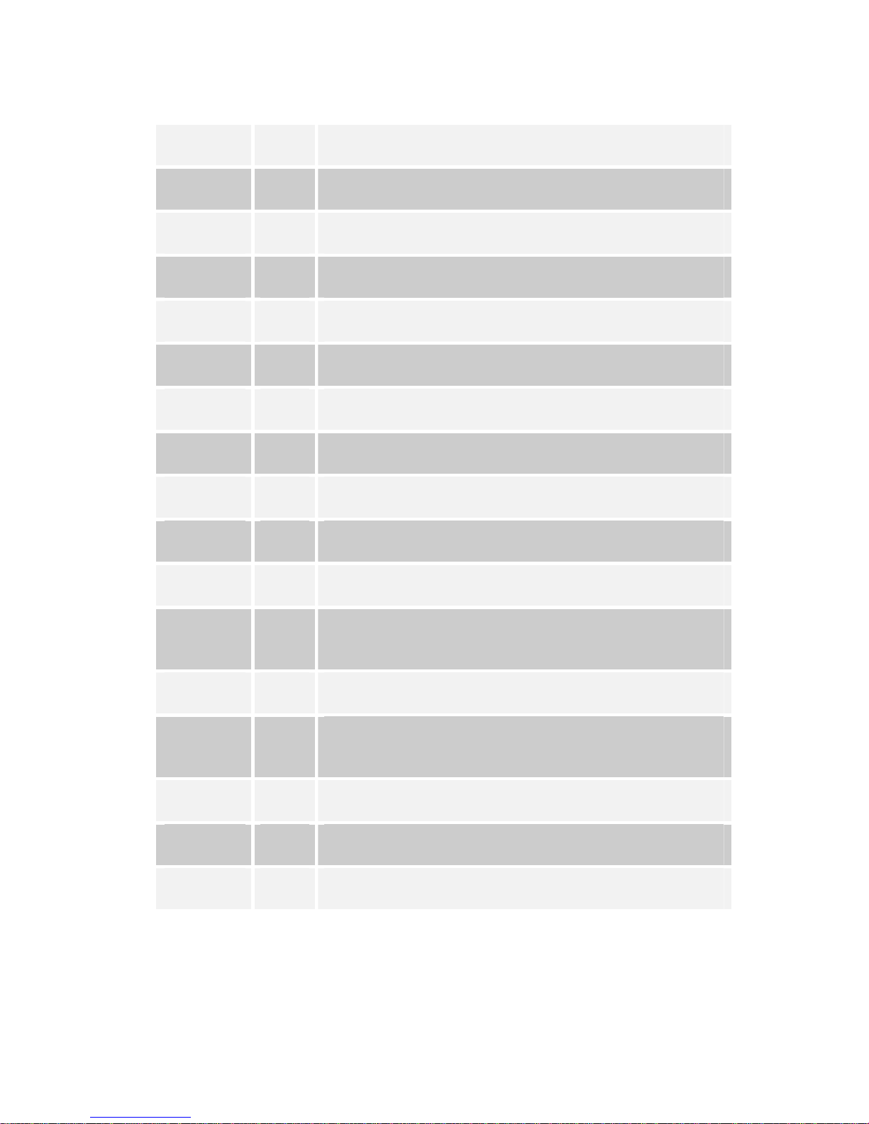
50 4 Frame Period in Pixel Clocks
54 4 Exposure Delay in Pixel Clocks
58 2 Serial Link Bit Period in Pixel Clocks
60 1 Camera Link Readout Mode
61 1 Camera Link Clock Frequency
62 1 Binning
63 1 Memory Options
64 1 Sensor Resolution - 8/10 bit
65 2 Trigger Mode (2nd Byte is Data FPGA dependent)
67 1 Frame count for Multi-Trigger mode
68 1 CC Mode: CC2, CC3, CC4 enable and edge select
69 59
Reserved for Control FPGA / base system
extension
128 2 Post-Trigger frame count (0 to 65535)
130 1
Debug Byte (for scoping Memory FPGA internal
signals)
131 1 Readback_count (1 to 255)
132 2 Vertical Blanking for USB “frame” (2 to 3613)
134 378 Available for Data FPGA functionality extensions
Table 4 - Camera State Memory Layout
40
Page 41

Sensor reference voltages are presented to the DAC's exactly as they are stored in the
state. The order listed above is the recommended order, but other orders may work. The
format for these is MS byte first with the most significant nibble indicating the command
code to the DAC. Pairs of values are sent, one to each DAC chip with the first going to
U25 and the second to U26. Voltages are updated in the order sent. Default values
shown are for the FastCamera 13. For more information see the LTC1660 data sheet.
Whenever the state memory is updated from host or flash, the actual internal registers that
implement the camera state also change. Some of these are located in the Control FPGA
and some in the Data FPGA. The Control FPGA forwards state data to the Data FPGA
whenever it is updated.
The state memory holds all of the state variables currently defined for camera operational
modes as well as some additional storage that can be defined as required for more
sophisticated Data FPGAs. The Data FPGAs can count on this storage to be refreshed
from flash after initial FPGA load and whenever the user restores state from one of the
saved sets in flash.
In addition to the camera state storage pages, some of the flash memory is available for
Data FPGA storage requirements such as pixel defect maps. The amount of flash
available for this depends on the size of the Data FPGA and the size of the flash device. A
pointer in the flash header in page zero indicates the starting page of the Data FPGA
initialization area. Its length in pages (which may be zero) is stored in the flash header as
well. Data from this initialization area is read out and sent to the data FPGA after initial
FPGA load. Although the data in these pages has no predefined layout, the first page
must start with the sequence 3C, A5, 0F, 96. This prevents transmission of uninitialized
flash pages and serves to identify the following data as Data FPGA Initialization Data
rather than Camera State.
Serial Camera Control Interface
SERIAL CONTROL INTERFACE
Encoding
Commands and response use the 7-bit ASCII code zero-extended to 8 bits. This is
sometimes referred to as 8 bits, no parity or 7-bits space parity. For characters that
require escape codes as listed below, the 8th bit is significant in the decoding, so only the
normal character encoding needs to be escaped. For example hex 0d requires the escape
sequence but hex 8d does not.
41
Page 42

The data within a command or response packet may contain 8-bit binary data with
escaping as described below. The camera requires only one stop bit for framing and
sends one stop bit when responding.
Baud Rate
To comply with the Camera Link specification, the default baud rate is 9600. The serial
baud rate can be changed with a command on the serial link or via the USB port. To allow
recovery after inadvertent setting of a higher baud rate than the host can handle, the serial
link will revert to 9600 baud after 5 framing errors without receiving a valid command. The
factory default startup baud rate is 9600, but the actual power-on baud rate can be
changed via the user start-up settings.
Command Protocol
Commands all begin with a character in the range g-z or G-Z where the case is ignored.
Subsequent bytes of the command are command-specific, but most commands use hex
characters 0-9 and a-f or A-F for the subsequent bytes. For commands using the hex
encoding, all arguments are full bytes. Thus an odd number of hex digits are considered a
protocol error. For commands that use binary encoding, the following character
sequences are required:
Character (hex, ASCII) Sequence
0d, <cr> \<cr>
5c, \ \\
All commands end in a non-escaped carriage-return, hex 0d.
When commands take arguments in hex, data must consist of pairs of hex characters
representing full bytes. Within each byte the most significant nibble is sent first, but for
multi-byte values the least significant byte is normally sent first. Thus when a command
required a 32-bit value the string "23568912" would produce the hex value 12895623.
Commands using hex arguments will ignore space characters, so "23568912" is equivalent
to "23 56 89 12". Other characters will cause the command to abort and respond with
negative acknowledge at the next non-escaped carriage-return.
42
Page 43

The intent of the protocol is to allow hand typing of commands from a terminal except for
long commands like flash page write that would only be done using the FastVision camera
control GUI.
Response Protocol
Each command signals completion by sending the command character G-Z (always
uppercased) followed by any command-specific response and terminated with a nonescaped carriage-return, hex 0d. For commands that respond with binary data, the
carriage-return (0d) and backslash (5c) are escaped as in the command protocol.
If a command cannot be completed for any reason the response will be the character? (3F)
and possibly a numeric error code, followed by a carriage-return to indicate negative
acknowledge.
Here again the intent is to use ASCII only response except for long data sequences like
flash page read.
Synchronization
The ASCII format of most commands combined with the escaped carriage-return in binary
commands allows simple resynchronization after errors. Sending two carriage-returns will
always reset the serial link to its default state, waiting for new command.
In addition, when the serial logic detects a framing error or protocol error, it will go into an
idle state until the next non-escaped carriage-return. During the idle state any serial data
is ignored. Any carriage-return which follows the idle state causes the negative
acknowledge sequence to be sent.
Timeout
If the serial logic is in a state waiting for a command to be completed and no input is
detected for 5 seconds, it will reset to waiting for a new command state without sending
any response. This would typically happen after the serial link had noise from attaching or
restarting the frame grabber.
Command Forwarding
All commands are forwarded to the data FPGA. All responses from the data FPGA are
forwarded to the host. Starting commands on both the Control and Data FPGAs without
waiting for completion may cause interleaving of response codes.
Command Set Overview
43
Page 44

To simplify command processing, commands that are handled in the Control FPGA are
assigned in ascending order starting with "G," and commands for the Data FPGA are
assigned in descending order starting with "Z."
GET CAMERA STATE
This command takes no arguments. The camera responds with "G" followed by the
current running state of the camera (512 bytes as 1024 hex digits) and a carriage-return.
This can be used to synchronize the GUI with the camera at initial connection time.
Camera state is sent as hex ASCII unlike the flash page read. This is because the camera
state is a single page worth of data, but flash page read is likely to be used many times in
a row to read large amounts of data such as the FPGA bit-stream.
PING CAMERA
This command takes no arguments. The camera responds with "H" followed by eight hex
digits and a carriage-return. The eight hex digits indicate the value of a free-running 32-bit
frame counter. This counter indicates all frames read from the sensor since power on, not
necessarily the number of frames sent to the frame grabber. The number of grabbed
frames depends on the memory functions such as frame binning, FIFO and circular
buffering. Successive pings can be used for a rough estimate of the sensor frame rate.
RESTORE CAMERA STATE FROM FLASH
This command takes one argument. The argument can be 01 to 08 and indicates which of
the 8 flash storage areas to retrieve the camera settings from. If the flash storage area is
un-initialized the camera will send a negative acknowledge. Otherwise the camera
responds with "I" followed by the flash storage area number and a carriage-return. The
Restore Camera State from Flash command only restores user settable parameters other
than the Data FPGA loads.
INITIALIZE FPGA FROM FLASH
This command takes no arguments. The Data FPGA is reloaded from the flash causing a
complete re-initialization of the readout logic. If the FPGA fails to load for any reason, the
camera will send a negative acknowledge and response code. Otherwise the camera
responds with "J" followed by a carriage-return. Failure results when the DONE signal
does not go high after download, or if the INIT# signal is reasserted after the bit-stream
has started to load. Either of these conditions indicates a bit-stream error. The Control
FPGA does not check the bit-stream for correct format or CRC; this is done by the FPGA.
To reduce the timeout length if the J command is issued when the flash is un-initialized;
the bit-stream bit counter only loads the low 24 bits of the bit-stream length from the flash
header. This still allows up to 128 megabits of bit-stream, larger than the flash size. On
error a response code is returned. The first byte is the reason which may be 00 01 or 02.
00 indicates bad header flash part type. 01 indicates illegal starting page address. 02
indicate load was attempted but did not complete. If the code is 02, six additional bytes
44
Page 45
are sent indicating the number of bytes remaining when the operation aborted. This is
usually zero, unless the FPGA re-asserted the INIT line.
SAVE CURRENT CAMERA STATE TO FLASH
This command takes one argument. The argument can be 01 to 08 and indicates which of
the 8 flash storage areas to store the camera settings in. The camera responds with "K"
followed by the flash storage area number and a carriage-return. This command only
saves user settable parameters other than the Data FPGA loads (512 bytes total).
WRITE FLASH
This command takes arguments that form the precise command to send to the flash
memory. Data length is limited by the flash page buffer size. There is no equivalent write
command to "Continuous Array Read". The intent of the command is to allow uploading
the FPGA code and to write to flash areas that need to be initialized at the factory. The
data is not interpreted by the serial control logic. It is possible to use this command to
directly upload camera settings to the flash pages without changing the current camera
state.
This is the only Control FPGA command that uses binary encoded arguments (with escape
codes for <cr> and \). The exact syntax of the Write Flash command is:
'L' <opcode> <addr> <data> <cr>
where opcode is one byte, addr is 3 bytes, and data can be from zero to 528 bytes
depending on the command. The following opcodes are acceptable to use with this
command (there is no error checking so make sure these are the only codes used).
0x84 Buffer 1 write
0x87 Buffer 2 write
0x83 Buffer 1 to main memory program with built-in erase
0x86 Buffer 2 to main memory program with built-in erase
0x88 Buffer 1 to main memory program without built-in erase
0x89 Buffer 2 to main memory program without built-in erase
0x81 Page Erase
45
Page 46

0x50 Block Erase
0x82 Main memory page program through buffer 1
0x85 Main memory page program through buffer 2
The following non-write commands are also implemented with Write Flash:
0x53
0x55
0x60
0x61
0x58
0x59
Main memory Page to Buffer 1 Transfer
Main memory Page to Buffer 2 Transfer
Main memory Page to Buffer 1 Compare
Main memory Page to Buffer 2 Compare
Auto Page Rewrite through Buffer 1
Auto Page Rewrite through Buffer 2
The camera responds with "L" followed by a carriage-return. Internally the Control FPGA
waits for the flash to become non-busy then starts the flash write operation. It does not
wait for the flash to complete it (become not busy) after starting the command.
Subsequent flash operations check the busy state of the flash memory, allowing overlap of
serial communication and flash programming. Theoretically a flash write command without
initial wait could give even more overlap by allowing write to a non-busy buffer while a
previous write is ongoing, but in practice the flash page write timing is shorter than the
serial transmission time to send the command. At 115,200 baud it takes about 46 msec to
send 528 bytes. The flash page erase/write cycle is only 20 msec max.
READ FLASH
This command takes arguments that form the precise command to send to the flash
memory followed by the command length and data length to be read in bytes. Command
length includes any "don't care" bytes required by the flash command selected. Data
length is limited by the flash page buffer size for most commands, but can be as large as
46
Page 47

the entire array if the Continuous Array Read flash command is used. All arguments are
ASCII hex. The exact syntax of the Read Flash command is:
'M' <opcode> <addr> <cmd_len> <data_len> <cr>
where opcode is one byte (2 hex digits), addr is 3 bytes (6 hex digits), cmd_len is one byte
(2 hex digits), and data_len is four bytes (8 hex digits). Most commands send the
<opcode> and <addr> bytes to the flash and then require some number of "don't care"
bytes before starting to read data from the flash. The only exception is the status read
command which sends only the command byte and has no additional turn-around delay.
When sending the status read command the <addr> bytes are "don't care", but must be
included in the command arguments. The following opcodes are acceptable to use with
this command (there is no error checking so make sure these are the only codes used).
Opcode Command Command Length
D4 Buffer 1 read 5
D6 Buffer 2 read 5
E8 Continuous array read 8
D2 Main Memory Page Read 8
D7 Status Register Read 1
This is the only Control FPGA response that uses binary encoded arguments (with escape
codes for <cr> and \).
The camera responds with "M" followed by escaped binary data from the flash and finally a
non-escaped carriage-return. Internally the Control FPGA waits for the flash to become
non-busy then starts the flash read operation. Thus the Status Register Read command is
only useful to check the compare flag, since the busy flag will always be off.
SET CAMERA STATE
This command takes a two byte (4 hex digit) offset into the current camera state as defined
in Table 4 and from one to to 512 bytes (2 to 1024 hex digits) of camera state data. The
exact syntax of the Set Camera State command is:
47
Page 48

'N' <addr> <data> <cr>
where <addr> is 4 hex digits of offset per Table 4 and <data> is 2 to 1024 hex digits
(always a multiple of 2) of data which will be stored sequentially into the current camera
state as shown in Table 4. Actual registers affected by the command are updated as the
data comes in, except where further synchronization is required such as multibyte values
and values that change only between frames. The Control FPGA always responds with
"N" followed by a carriage-return even if the affected state is handled by the Data or DDR
FPGAs. If the baud rate is changed, the command response happens at the original baud
rate.
SERIAL TRIGGER
This command takes no arguments. This command has the same effect as pulsing the
CC1 line high for the time period between receipt of the 'O' and receipt of the carriagereturn. Although this command would normally be used only in edge-triggered mode, it
can also be used in external exposure mode for long exposures (minimum exposure is
limited by the serial baud rate). To support this mode, any characters between the "O" and
the <cr> are ignored. Thus the total command length in characters can be used to
determine the exposure time. The camera responds with "O" followed by a carriagereturn.
RESET AND CALIBRATE SENSOR
This command takes no arguments. It causes the sensor's LRST_N signal to be pulsed
low for two clock cycles. The sensor is reset and performs an auto-calibration. This
command is applied by the readout logic between frames. If enabled, the CC4 line will also
initiate this command allowing operation without the GUI. The camera responds with "P"
followed by a carriage-return.
SEND INITIALIZATION DATA TO DATA FPGA
This command takes any number of bytes (even number of hex digits) of FPGA
initialization data. The exact syntax of the Send Initialization Data command is:
'X' <data> <cr>
where <data> is an even number of hex digits of data which can be used for any function
required by the Data FPGA. This command is sent by the Control FPGA to the Data
FPGA upon power-on initialization and after the 'J' command (Initialize FPGA from Flash).
It is also possible for the host to issue this command via the Camera Link serial interface,
but be aware that the Data FPGA does not issue a response.
READOUT IMAGE
48
Page 49

This command can take no arguments or it can take a 32-bit (8 hex digits) address. This
command is only effective in the memory readout modes. If enabled, the CC2 line will also
initiate this command allowing operation without the GUI. The Data FPGA will respond
with "Y" followed by a carriage-return.
RESET MEMORY
This command takes no arguments. This command is only effective in the memory
readout modes. If enabled, the CC3 line will also initiate this command allowing operation
without the GUI. The Data FPGA will respond with "Z" followed by a carriage-return.
Inter-FPGA Communications
SERIAL COMMANDS
Commands from the host are buffered and passed to the Data FPGA on the FPGA_CTL3
wire. The Data FPGA therefore receives all commands from the host and can act on them
accordingly. This allows extensions to be made to the command set for Data FPGA use.
To reduce logic in the Data FPGA, each character is buffered and retransmitted at 66
MHz, synchronous to the FPGA_SYSCLK. In this way the data FPGA doesn't need to
know about baud rate and can start up monitoring commands even before it receives the
camera state data.
FLASH DATA
In addition to forwarding commands from the host, the Control FPGA also uses the
FPGA_CTL3 wire to send camera state data when the Restore Camera State from Flash
command is received. It also uses the FPGA_CTL3 wire to send camera state data and
Data FPGA initialization data from flash to the Data FPGA when the Initialize FPGA from
Flash command is received. The Control FPGA only responds to the host after it has
completed the required data transfer(s). The host must always wait until it receives the
response before sending another command.
When transmitting camera state data to the Data FPGA, the Control FPGA uses the same
syntax as the Set Camera State command with the starting address set to zero and a data
length of 512.
When transmitting Data FPGA initialization data to the Data FPGA, the Control FPGA uses
the same syntax as the Set Camera State command with the starting address set to all
ones (65,535) and a data length as set in the Page Zero Flash Header. If the header
indicates a zero data length, or the initialization data does not start with 3C A5 0F 96, the
Control FPGA will not send this command.
SERIAL RESPONSES
49
Page 50

Normally the data sent to the Data FPGA from the Control FPGA is limited in bandwidth at
the source, either by the host serial baud rate or the flash memory read rate. Response
data from the Data FPGA, which always gets forwarded to the host, must be sent at the
host baud rate. To reduce the redundant logic requirement in the Data FPGA, the Control
FPGA uses the FPGA_DDRCLK wire to send a baud rate pulse train. This signal is high
for one cycle of FPGA_SYSCLK once per serial link bit period. The Data FPGA then uses
this as a shift enable for its response transmitter.
Serial response data from the Data FPGA is forwarded to the host directly by ANDing with
the serial response data from the Control FPGA. For this reason it is especially important
that the host does not send a new command before the previous command response has
been received.
Embedded Soft Processor Core
The Control FPGA includes a "PicoBlaze" 8-bit controller core, programmed in assembly
language, which takes care of most low-speed complex operations. This soft processor
handles serial protocol, flash memory, FPGA configuration, and power-on initialization.
The architecture of this core is Harvard, using a 1K by 18-bit wide instruction memory
composed of 5 block RAMs, and a 1K by 8-bit wide data memory composed of four block
RAMs. The core was designed and optimized to run in the Virtex 2 series of Xilinx FPGAs
and then adapted for the Spartan 2. It therefore is not very fast. In the MV13 it runs at 33
MHz and in the MV40 it runs at 25 MHz (1/2 the pixel clock rate). The instructions run in a
fixed 2-cycle period with essentially no pipelining. This simplifies instruction sequence
timing calculations.
The PicoBlaze data address space is only 256 bytes. If you look at the processor
documents from Xilinx you'll find this called I/O rather than data. In our case the data
space connects to 1K bytes of internal block RAM using three additional banking bits
implemented as register. Access to the entire 1K of RAM as well as 8 registers is
accomplished with some stunt logic. Registers normally appear at addresses 0xf8 through
0xff regardless of the state of the three banking bits. When register access is enabled,
writes are shadowed in the block RAM at 0x6f8 through 0x6ff regardless of the state of the
three banking bits. Register access can be disabled by reading or writing location 0xf7
and re-enabled by reading or writing locations 0 through 0xf6. In this manner a program
can sequentially access the entire RAM by temporarily disabling register access. A special
bit, bit 0 of register 0xff, toggles each time any read is performed. This allows a simple test
of the current state of the register access enable by reading location 0xff twice and
comparing the two values.
The high 256 bytes, from 0x700 through 0x7ff, are dual-ported with the I2C slave unit.
This provides a simple interface for introducing commands via USB. The interface uses
three sub addresses, 0x60 0x61 and 0x62. Writes by the USB host to 0x60 are treated the
same as characters on the serial line (SERTC). The PicoBlaze has a status bit, bit 4 of
register 0xFC, that indicates when new data is available from the USB host. When the
50
Page 51

PicoBlaze reads the data at sub address 0x60 this status bit is cleared. The USB host
does not have a similar status bit; however it can be safely assumed that the PicoBlaze will
process characters as fast as they come in, as long as no transmission occurs between
the carriage-return that completes a command and the receipt of the carriage-return that
completes the response to that command. When the PicoBlaze starts its response to the
host, the first character of the response is written to sub address 0x61 and the value 0x01
is written to sub address 0x62. The PicoBlaze has another status bit, bit 4 of register
0xFC, which indicates when the host has read the value in sub address 0x61. The bit is
set when response data is written by the PicoBlaze and cleared when it is read by the USB
host. Once the host has read each response byte, the PicoBlaze continues to place new
characters at sub address 0x61 until the message is completed with an unescaped
carriage-return. The host can assume that once the value 0x01 is in sub address 0x62 it
can continue to read characters from 0x61 as fast as it can until it receives a carriagereturn. When the PicoBlaze has finished the response, it writes 0x00 to sub address 0x62
and returns to the host service loop.
"FGET8" SPEED-UP LOGIC
Because the PicoBlaze runs relatively slow, there is a small sequencer to speed up FPGA
configuration and flash data read. This is kicked off by a write to register 0xfe with bit 6
set. The sequencer runs the flash clock for 8 cycles, and if the FPGA CCLK was high,
copies the flash DOUT output to the FPGA configuration DIN input cycling the FPGA
CCLK 8 cycles as well. The PicoBlaze is responsible for making sure the flash is in the
appropriate state when this sequencer is started. Generally it only speeds up the inner
loop of FPGA configuration and flash data read, but this is where the largest time is spent.
Using the algorithm from previous PicoBlaze designs (Video Combiners) and bit wiggling,
the best data rate for FPGA download would be about 1.5 MHz for CCLK. With the
"Fget8" speed-up logic the rate should be about 9 MHz. This allows even large FPGAs to
be loaded in less than 2 seconds.
PICOBLAZE MEMORY MAP
Address Description
000 - 1FF
200 - 3FF
400 - 6F7 Working memory for host commands.
Camera state storage. Sensor registers
shadow locations in 000 - 0FF
Header storage. Loaded from flash page 00
at power-up.
51
Page 52

6F8 - 6FF
Register shadow memory for read back of
otherwise write-only bits.
700 - 7FF I2C shared area.
PICOBLAZE REGISTER MAP
All of the following registers can only be accessed when the register access enable signal
is set. This is accomplished by making any access to locations 00 through 0xf6. Any
access to location 0xf7 clears the register access enable signal. Accesses within the 0xf8
through 0xff register area do not affect the state of the register access enable signal.
0XF8 BAUD RATE PERIOD, LOW 8 BITS AND FRAME COUNT.
0XF9 BAUD RATE PERIOD, HIGH 8 BITS AND FGET8 DATA.
The Baud rate is derived by dividing the pixel clock frequency by the number entered here.
In the MV13, the pixel clock runs at 66.667 MHz and the default setting for 9600 baud
would be 6944. The last value written to the Baud Rate high 8-bits register can be read
back from scratchpad location 0x2f9 when register access is disabled. When register
access is enabled, reading 0xF9 returns the byte of flash data from the "Fget8" sequencer.
Reading 0xF8 returns the frame count in four successive reads. Frame count is latched
whenever address 0x00 is read.
0XFA SENSOR CONTROL.
The Bits are:
Bit 7 Read-only "Y" pending. Indicates that a CC2 event has occurred and the
PicoBlaze should forward it to the Data FPGA as a "Y" command.
Bit 6 Read-only "Z" pending. Indicates that a CC3 event has occurred and the
PicoBlaze should forward it to the Data FPGA as a "Z" command.
Bit
Reserved.
5
Bit Serial trigger. Must be toggled in software to trigger the sensor control logic in
52
Page 53

4 response to a serial trigger command
Bit
Reserved.
3
Calibrate sensor. This is a pulsed signal that schedules a calibration when this
bit is written to 1. Writing this bit to zero has no effect. Actual calibration may
Bit
2
happen much later, since the sensor control logic schedules calibration only
between frames.
Bit 1 Sensor standby. Setting this bit to one places the sensor in low-power
standby mode
Bit 0 Dark offset enable. Setting this bit allows the sensor to apply internal
calibration factors to reduce fixed column noise.
0XFB ADDRESS EXTENSIONS.
Bits 3 through 7 are reserved. Other bits are:
Bits 2, 1, 0 Banking bits. These bits form the two high address bits to the 1K byte data
RAM, except during register access. During register access the high bits are fixed at 6,
thus register writes are always shadowed in the 7th of 8 banks, allowing read back of
registers that don't have separate read functionality from the shadow RAM. When bank 0
is selected, sensor register write is enabled.
0XFC SERIAL TO FPGA AND SERIAL STATUS.
When written, this register causes a byte of data to be transmitted to the Data FPGA. On
reads Bits 0 through 3 are reserved. Other bits are:
Bit 7 Transmitter to FPGA ready for data.
Bit 6 Transmitter to FPGA overrun error. Set if write was attempted when the transmitter
wasn't ready for data. Cleared when the next data is written when the transmitter is ready
for data.
Bit 5 Transmitter to USB host busy (transmit data available). Set when the PicoBlaze
writes to offset 0x61 in the USB shared area (page 7). Cleared when the data is read by
the USB host via I2C.
Bit 4 Receiver from USB host has data available. Set when the USB host writes to sub
address 0x60 via I2C. Cleared when the data is read by the PicoBlaze at offset 0x60 in
the USB shared area.
53
Page 54

0XFD UART TO/FROM CAMERA LINK.
Writing this location sends a byte of serial data to the frame grabber. Reading gets a byte
of serial data and acknowledges its receipt. See the status bit descriptions below for more
information.
0XFE DAC AND FLASH CONTROL / FLASH AND UART STATUS.
The Bits are:
Bit 7 Reserved on write, RxData Available on read. When this bit is 1, there is data
available to be read from the UART via register 0xFD. The validity of the current data
depends on the error bits listed below. This and other receive status bits are cleared when
the UART is read.
Bit 6 "Fget8" on write, Transmitter Ready on read. Writing this bit to one starts the
sequencer for speeding up flash read and FPGA configuration write. Writing this bit to
zero has no effect. When 1 this bit indicates that the UART is ready to accept a byte of
data to transmit to the frame grabber.
Bit 5 DAC chip select on write, Receiver framing error on read. DAC chip select is
asserted high. This bit is inverted before driving the chip's active low pin. Receiver
framing error indicates that a zero was detected in the stop bit position. This condition is
cleared when the UART is read.
Bit 4 DAC serial clock on write, Receiver overrun error on read. DAC serial clock runs
directly to the DAC chips. Receiver overrun indicates that a new character came in when
the previous character had not been read. In this case the older data is lost and the data
in the UART is the one causing the overrun, i.e. the most recent character received. This
condition is cleared when the UART is read.
Bit 3 Flash chip select on write, Transmit overrun on read. Flash chip select is asserted
high. This bit is inverted before driving the chip's active low pin. Transmit overrun is set if
a write was attempted when the transmitter wasn't ready for data. This condition is cleared
when data is written to the UART and the transmitter is ready for data.
Bit 2 Flash reset on write, transmitter empty on read. Flash reset is asserted high. This
bit is inverted before driving the chip's active low pin. Transmitter empty is active when no
data transmission is pending. This must be checked before changing the baud rate to
ensure any pending characters finish transmitting at the current baud rate.
Bit 1 Flash serial clock on write, Flash ready on read. These correspond directly to the
flash pin functions.
Bit 0 Shared Flash and DAC serial data in on write, Flash data out on read. These
correspond directly to the respective pin functions.
54
Page 55

0XFF FPGA CONFIGURATION.
The bits are:
Bit 7 Read only "Fget8" status. This is high when the sequencer is still running from a
prior operation.
Bit 6 is reserved.
Bit 5 FPGA Loaded on write, FPGA done on read. Writing this bit high indicates that the
program has finished loading the data FPGA and enables the pinsaver muxes. FPGA
Done is the configuration pin function.
Bit 4 FPGA M1 on write, FPGA INIT on read. M1 is the configuration mode bit. Other
mode bits are pulled up. Writing 1 sets the Data FPGA into slave serial mode for
configuration load by the Control FPGA. Writing 0 sets the Data FPGA into JTAG mode
for configuration by external Xilinx Parallel Cable. FPGA Init is inverted from the active low
configuration /INIT pin.
Bit 3 Read only FPGA Data Out. This allows read back functions to be implemented in
the future.
Bit 2 Write only FPGA Program. This bit is inverted before driving the chip's active low
pin. Setting this bit to 1 resets the Data FPGA configuration.
Bit 1 FPGA Configuration Clock on write, Configuration Timeout on read. Writing this bit
directly affects the FPGA CCLK pin except when the "Fget8" sequencer is running. In that
case this bit enables Flash to FPGA data transfer if it is 1. Running "Fget8" while this bit is
0 will not cause any changes to the FPGA DIN or CCLK signals. Configuration Timeout
goes high if there have been 16,777,216 CCLK clocks since Program was last asserted.
This can be used as a simple timeout mechanism for a program that only checks the Done
and Init status during FPGA configuration.
Bit 0 FPGA Data In on write, Access Test Bit on read. During FPGA configuration this is
the serial data to the Data FPGA. After configuration it could be used as an additional
control line to the Data FPGA. The Access Test Bit toggles on any port read. Thus
reading this register twice in a row will always provide different data. This can be used to
test whether the register access enable signal is active.
SENSOR REGISTER MAP
All of the following registers can only be accessed when the sensor register write enable
signal is set. This is bit 2 of register 0xfb. Writing these registers will also cause the
values to be shadowed in the scratchpad RAM at whatever page is currently indicated by
bits 1 and 0 of register 0xfb. Thus although the registers themselves are write-only, there
is a copy in the scratchpad RAM immediately after writing them. The scratchpad copy can
55
Page 56

obviously be overwritten without affecting the sensor registers if the sensor register write
enable bit is off. The layout of these registers intentionally matches the flash state storage.
0X24 START PIXEL, LOW 8 BITS.
0X25 START PIXEL, HIGH 8 BITS.
This is the leftmost pixel in the ROI. Pixels are numbered from 0 to the sensor width - 1.
This is different from the old ROI settings which worked in pixel clocks. The sensor control
logic handles the conversion from pixels to clocks. If the starting pixel is not a multiple of
the sensor readout width (10 for MV13 or 16 for MV40) there will be some prescan pixels
in the resultant image. In the future we may want to add logic in the data FPGA to mask
out the prescan pixels.
0X26 END PIXEL, LOW 8 BITS.
0X27 END PIXEL, HIGH 8 BITS.
This is the rightmost pixel in the ROI. Pixels are numbered from 0 to the sensor width - 1.
This is different from the old ROI settings which worked in pixel clocks. The sensor control
logic handles the conversion from pixels to clocks. If the ending pixel is not one less than
a multiple of the sensor readout width (10 for MV13 or 16 for MV40) there will be some
postscan pixels in the resultant image. In the future we may want to add logic in the data
FPGA to mask out the postscan pixels.
0X28 START LINE, LOW 8 BITS.
0X29 START LINE, HIGH 8 BITS.
This is the top line in the ROI. Lines are numbered from 0 to the sensor height - 1. Only
lines in the ROI are scanned.
0X2A END LINE, LOW 8 BITS.
0X2B END LINE, HIGH 8 BITS.
This is the bottom line in the ROI. Lines are numbered from 0 to the sensor height - 1.
Only lines in the ROI are scanned.
0X2C LINE PERIOD, LOW 8 BITS.
0X2D LINE PERIOD, HIGH 8 BITS.
56
Page 57

This is the line readout time in pixel clocks - 1. I.e. the actual period is one clock more
than this number.
0X2E EXPOSURE PERIOD, BITS <7:0>
0X2F EXPOSURE PERIOD, BITS <15:8>
0X30 EXPOSURE PERIOD, BITS <23:16>
0X31 EXPOSURE PERIOD, BITS <31:24>
This is the desired exposure time in pixel clocks. Actual exposure time may vary,
especially if readout overlaps exposure.
0X32 FRAME PERIOD, BITS <7:0>
0X33 FRAME PERIOD, BITS <15:8>
0X34 FRAME PERIOD, BITS <23:16>
0X35 FRAME PERIOD, BITS <31:24>
This is the desired frame readout period in pixel clocks - 1. I.e. the actual period is one
clock more than this number.
0X36 DELAY PERIOD, BITS <7:0>
0X37 DELAY PERIOD, BITS <15:8>
0X38 DELAY PERIOD, BITS <23:16>
0X39 DELAY PERIOD, BITS <31:24>
This is the desired delay from trigger to exposure in edge-triggered modes. It is not used
in free-running or external exposure modes. Actual exposure delay may vary, especially if
readout overlaps exposure.
0X41 TRIGGER MODE.
Bit 7 is reserved. Other bits are:
57
Page 58

Bit 6 Invert TTL Trigger. Setting this bit to 1 indicates the TTL trigger input on P2 is
active low level, or falling edge.
Bit 5 Enable TTL trigger. Set this bit to 1 to enable TTL trigger input on P2. Clear to 0 to
disable TTL trigger input.
Bit 4 Synchronous Exposure. This bit only affects free-run and multi-frame edgetriggered modes. When this bit is set, the readout timing is synchronized to the exposure.
Bit 3 Invert Camera Link CC1 Trigger. Setting this bit to 1 indicates the CC1 trigger input
on Camera Link is active low level, or falling edge.
Bit 2 Enable Camera Link CC1 trigger. Set this bit to 1 to enable CC1 trigger input on
Camera Link. Clear to 0 to disable CC1 trigger input.
Bit 1:0 Trigger Mode.
0 Free-running mode.
1 Multi-frame edge-triggered mode.
2 Single edge-triggered mode.
3 External exposure mode.
0X43 TRIGGER COUNT.
Total number of frames to capture in multi-frame edge-triggered mode. 0 to 255 program
0 to 255 frames.
0X44 CC MODE
Enable and active edge of CC2, CC3, and CC4 command inputs. Bits 7, 6 are reserved.
Other bits are:
Bit 5 Invert CC4. Setting this bit to 1 indicates the CC4 input is active on falling edge.
Setting this bit to 0 indicates the CC4 input is active on rising edge.
Bit 4 Enable Camera Link CC4. Set this bit to 1 to enable CC4 Sensor Calibration.
When enabled, the active edge of CC4 causes the sensor to be reset and calibrated at the
next appropriate time.
Bit 3 Invert CC3. Setting this bit to 1 indicates the CC3 input is active on falling edge.
Setting this bit to 0 indicates the CC3 input is active on rising edge.
Bit 2 Enable Camera Link CC3. Set this bit to 1 to enable CC3 Reset Memory. When
enabled, the active edge of CC3 causes the memory to be reset.
58
Page 59

Bit 1 Invert CC2. Setting this bit to 1 indicates the CC2 input is active on falling edge.
Setting this bit to 0 indicates the CC2 input is active on rising edge.
Bit 0 Enable Camera Link CC2. Set this bit to 1 to enable CC2 Readout Image. When
enabled, the active edge of CC2 causes the current memory image to be read out.
DATA FPGA
This version of the data FPGA is very simplified compared to other version of the camera.
It provides for basically two functions. Raw Data is passed from the sensor to the DDR
FPGA untouched.
Data coming back from the DDR FPGA is sent to the USB port, and the camera link port.
These two ports get essentially the same data. The image format is fixed for these two
ports; it is 642 by 482 eight bit pixels.
None of the other features (such as binning) of the data FPGA are supported. The camera
can essentially take images, pass them to the USB and the camera link, for preview, and
then record programmable image sizes and produce 16 bit TIFF files from the recording.
More features may come later, and as the Data FPGA can be programmed in the field via
the serial port or USB, the camera can be updated in the field.
DDR FPGA
REVISION 1.0 LIMITATIONS :
This revision of the Memory FPGA only implements memory in the storage and playback
modes. Future FPGA revisions may add frame averaging, image scaling, and look-up
table modes.
Data from the data FPGA to the memory FPGA runs at the sensor bandwidth, but data
from the memory FPGA back to the data FPGA only runs at the USB output bandwidth.
Memory is clocked at 100 MHz (200 Mbit DDR), instead of 133 MHz.
Recording Modes
Three modes are defined by the Control FPGA specification as “Direct from the Sensor,”
“FIFO Memory Mode,” and “Circular Buffer Memory Mode” with values of 0, 1, and 2
respectively in the Memory Options register (now at offset 63). Only the low three bits of
this register select the mode. Bit 3 of the Memory Options register is defined as the
preview bit, when set the camera outputs to USB the last frame written to memory. Bit 4 of
the Memory Options register when set (bit 3 must be zero), causes the camera to output
the first frame found after the address selected by the Y command. This is used in the
VCR function of the software. The mode bits are implemented as follows:
59
Page 60

DIRECT FROM THE SENSOR-MEMORY OPTIONS[2:0] = 0
Sensor data is written continuously to memory with each frame overwriting the previous
frame at memory location zero. If preview bit is enabled, readout to the USB runs
continuously at the maximum rate of the USB port with no attempt to synchronize to the
incoming frame rate. Use this mode for alignment and focus.
FIFO MEMORY MODE – MEMORY OPTIONS[2:0] = 1
Sensor data is written to memory starting at address zero when the memory is reset by the
Z command. If preview bit is enabled, readout to the USB is sequential from location zero;
pausing if the readout catches up to the write pointer. Writing is permanently disabled until
the next Z command if the write pointer reaches the read pointer (or if it wraps to zero if
preview is disabled).
CIRCULAR BUFFER MEMORY MODE – MEMORY OPTIONS[2:0] = 2
This is the most flexible mode for capture of short-lived high-speed events. Sensor data is
written to memory when enabled by sending the “Reset Memory” (Z) command. Writing to
memory continues in a circular buffer until a trigger is received. Following the receipt of
trigger the writing continues for up to 65535 frames as defined by the Post-Trigger Frames
register. Writing will not continue until re-enabled with another Z command.
If preview bit is enabled, readout to the USB is from the most recent frame as in Direct
Mode. Otherwise, reading only occurs when requested with the “Readout Memory” (Y)
command. Readout in this mode is random access, allowing re-read when USB
bandwidth is not available.
Details of Implementation:
STORAGE FORMAT
Each memory word has 118 usable bits. The low 100 data bits (bits 99:0) represent 10 10bit pixels as received from the data FPGA (in this version directly from the sensor without
binning). Bit 100 is Frame Valid. Bit 101 is Line Valid. Bit 102 is Data Valid (always 1).
Data is stored when Frame Valid and Line Valid are both 1, or when either of these signals
first becomes 0. This provides the framing required for continuous readout.
At the beginning of each frame, a word is inserted with the data bits replaced with frame
identification as follows. Bits 31:0 are the frame number as reported by the H command.
This increments with each exposure from the time the camera is turned on. Bits 63:32 are
the time in microseconds at the end of the frame's exposure as recorded in the control
FPGA. This time starts at 0 when the FPGA is loaded and wraps back to 0 about every
71.5 minutes. Bit 96 is 1 if a trigger event occurred between the end of the previous
exposure and the end of this one. All of this information is transmitted by the control FPGA
60
Page 61

via the Frame Valid line. Bits 95:64 are the starting address of the previous frame in
memory. This is a block address, not a byte address. Because of treating the DDR data
as SDR at 128 bits wide, a “word” is 16 bytes. The block to be read always starts at a 16
word boundary, thus the minimum addressable unit is 256 raw bytes of memory. Bits
102:100 for the frame ID word is always encoded as 110, Data Valid and Line Valid, but
not Frame Valid.
READING OUT MEMORY
Whenever the preview bit is enabled, only image data is sent to the USB and it is framed
as defined by the input ROI. The preview image is not scaled. The upper left corner of the
image will always be in the upper left corner of the preview, and excess image data will be
cropped to the 640 by 480 preview window. Image data is 8 bits per pixel using the most
significant 8 bits of the sensor data. The top left pixel is replaced with the readout status
byte as described below. If there are fewer than 640 pixels per line, lines are extended by
repeating the last 10 active pixels. Images are extended to include the top of the next
frame when there are fewer than 480 lines.
When the preview bit is not set, data is presented to the USB 300K bytes at a time. This
represents the 640 by 480 “frame” of the emulated HV7131 sensor; however the data is to
be interpreted as a raw stream by the host. The readout is initiated by the “Y” command in
one of two formats. The first format has no argument, just “Y” followed by a carriagereturn. In this format the returned data starts at the “current” address in memory. The
current address is initialized to the start of the most recently captured frame while memory
storage is active. The second format consists of “Y” followed by four bytes (8 hex digits) of
address, low byte first. This form directs the memory to return data starting at the
specified address. Note that only 22 bits of address are required for a 1 gigabyte SODIMM.
Either form of “Y” command can cause multiple 300K blocks to be sent per command.
This is controlled by the readback_count in configuration byte 131. Setting this byte to 0 or
1 sets one block per “Y” command. 2 to 255 blocks are programmed by setting
readback_count to the desired number of blocks.
Each 300KB block starts with 4 bytes indicating the starting address of the block. For the
second format of the “Y” command this should correspond to the requested address.
Following the start address are 23,616 words of memory (1,476 blocks). Thirteen bytes of
each word are transmitted, least significant byte first. After the last block are four more
bytes with the address of the next block. If the readback_count is greater than 1 this will
be the “current” address for the next block. The remaining 184 bytes are filled with the
current readout status byte. The readout status byte is defined as follows:
STATUS BYTE BITS DESCRIPTION
61
Page 62
Bit 7 This bit is 1 whenever the memory is enabled for writing new frames. This includes
any time the memory mode is programmed for direct or FIFO, and in circular buffer mode
from the time memory is reset (Z command) until all post-trigger frames have been written
to memory. Use this as the busy bit in circular buffer mode.
Bit 6 This bit is 1 if a trigger event has been received since memory reset.
Bit 5 This bit is 1 if the current 300KB USB frame contains a start of frame.
Bit 4 This bit is 1 if the entire memory has filled since the last memory reset. In circular
buffer mode this indicates a “wrap” condition. When this bit is set, the oldest frame in
memory can be found by scanning forward from the most recent frame. If the bit is not set,
the oldest frame will start at memory address zero.
Bits 3:0 These bits show the current state of the Memory Options register.
CONFIGURATION MEMORY CHANGES
The follow configuration for memory locations where added:
Byte Offset
(decimal)
Bytes Description
63 1 Memory Mode
128 2 Post-Trigger frame count (0 to 65535)
130 1
Debug Byte (for scoping internal
signals)
131 1 Readback_count (1 to 255)
132 2
Vertical Blanking for USB “frame” (2 to
3613)
The Memory Mode is a bit field in which
Bits 2-0 define the recording mode (circular buffer is mode 2)
Bit 3 1=preview the latest frame 0=don't preview
62
Page 63

Bit 4 1=preview the selected frame (Y command address). (Bit3=0)
The Read back count determines how many frames are returned by each Y command
when bits 3 and 4 of the Memory mode are zero. Zero and one give you 1 frame for each
command, 2 through 255 give you more. When the camera is reading out the images to
write tiff files this is set to 16.
The Vertical Blanking for USB time determine how many line times of delay are provided
between sending each video frame over USB, both for data and display. This can be used
to tune the delivery of data to the host. It is set to 2 in the software.
63
Page 64

TROUBLESHOOTING
There are several things you can try before you call FastVision Technical Support for help:
_____ Make sure the computer is plugged in. Make sure the power source is on.
_____ Go back over the hardware installation to make sure that the system is properly
installed.
_____ Go back over the software installation to make sure you have installed all
necessary software.
_____ Review your FastCamera Test Data CD to review correct camera configuration.
_____ Run the user-diagnostics test for your computer main board to make sure it’s
working properly.
_____ Insert the FastVision CD-ROM and check the various Release Notes to see if there
is any information relevant to the problem you are experiencing.
FASTVISION TECHNICAL SUPPORT
FastVision offers technical support to any licensed user during the normal business hours
of 9 a.m. to 5 p.m. EST. We offer assistance on all aspects of processor board and PMC
installation and operation.
CONTACTING TECHNICAL SUPPORT
To speak with a Technical Support Representative on the telephone, call the number
below and ask for Technical Support:
Telephone: 603-891-4317
If you would rather FAX a written description of the problem, make sure you address the
FAX to Technical Support and send it to:
Fax: 603-891-1881
You can email a description of the problem to [email protected]
Before you contact technical support have the following information ready:
_____ Serial numbers and hardware revision numbers of all of your products. This
information is written on the invoice that was shipped with your products.
64
Page 65

_____ Also, each product has its serial number and revision number written on either in ink
or in bar-code form.
_____ The version of the FASTVIEWER software that you are using.
_____ The type and version of the host operating system, i.e., WindowsXP.
_____ Note the types and numbers of all your software revisions
_____ Returning Products for Repair or Replacements
Our first concern is that you be pleased with your FastVision products.
If, after trying everything you can do yourself, and after contacting FastVision Technical
Support, you feel your hardware or software is not functioning properly, you can return the
product to FastVision for service or replacement. Service or replacement may be covered
by your warranty, depending upon your warranty. The first step is to call FastVision and
request a “Return Materials Authorization” (RMA) number. This is the number assigned
both to your returning product and to all records of your communications with Technical
Support. When a FastVision technician receives your returned hardware or software he
will match its RMA number to the on-file information you have given us, so he can solve
the problem you’ve cited.
When calling for an RMA number, please have the following information ready:
_____ Serial numbers and descriptions of product(s) being shipped back
_____ A listing including revision numbers for all software, libraries, applications, etc.
_____ A clear and detailed description of the problem and when it occurs
_____ Exact code that will cause the failure
_____ A description of any environmental condition that can cause the problem
All of this information will be logged into the RMA report so it’s there for the technician
when your product arrives at FastVision. Put boards inside their anti-static protective bags.
Then pack the product(s) securely in the original shipping materials, if possible, and ship
to:
65
Page 66

FastVision LLC.
71 Spit Brook Road, Suite 200
Nashua, NH 03060 USA
Clearly mark the outside of your package:
Attention RMA #90XXX
Remember to include your return address and the name and number of the person who
should be contacted if we have questions.
REPORTING BUGS
We at FastVision are continually improving our products to ensure the success of your
projects. In addition to ongoing improvements, every FastVision product is put through
extensive and varied testing. Even so, occasionally situations can come up in the fields
that were not encountered during our testing at FastVision.
If you encounter a software or hardware problem or anomaly, please contact us
immediately for assistance. If a fix is not available right away, often we can devise a workaround that allows you to move forward with your project while we continue to work on the
problem you’ve encountered.
It is important that we are able to reproduce your error in an isolated test case. You can
help if you create a stand-alone code module that is isolated from your application and yet
clearly demonstrates the anomaly or flaw.
Describe the error that occurs with the particular code module and email the file to us at:
We will compile and run the module to track down the anomaly you’ve found.
If you do not have Internet access, or if it is inconvenient for you to get to access, copy the
code to a disk, describe the error, and mail the disk to Technical Support at the FastVision
address below.
If the code is small enough, you can also:
FAX the code module to us at 603-891-1881
If you are faxing the code, write everything large and legibly and remember to include your
description of the error.
66
Page 67

When you are describing a software problem, include revision numbers of all associated
software.
For documentation errors, photocopy the passages in question, mark on the page the
number and title of the manual, and either FAX or mail the photocopy to FastVision.
Remember to include the name and telephone number of the person we should contact if
we have questions.
FastVision LLC.
131 Daniel Webster Highway, #529
Nashua, NH 03060 USA
Telephone: 603-891-4317FAX: 603-891 -1881
Web site: http://www.Fast-Vision.com/
Email: [email protected], or [email protected]
67
 Loading...