

Fairchild Semiconductor USB100N24, USB100N18, USB100M20, USB100AN24, USB100AN18 Datasheet
1
www.fairchildsemi.com
USB100 Programmable Low-Cost USB Machine (PLUM)
USB100 rev.D
USB100
Programmable Low-Cost USB Machine (PLUM)
Single Chip Controller for Mouse, Trackball, Joystick and Gamepad Applications
General Description
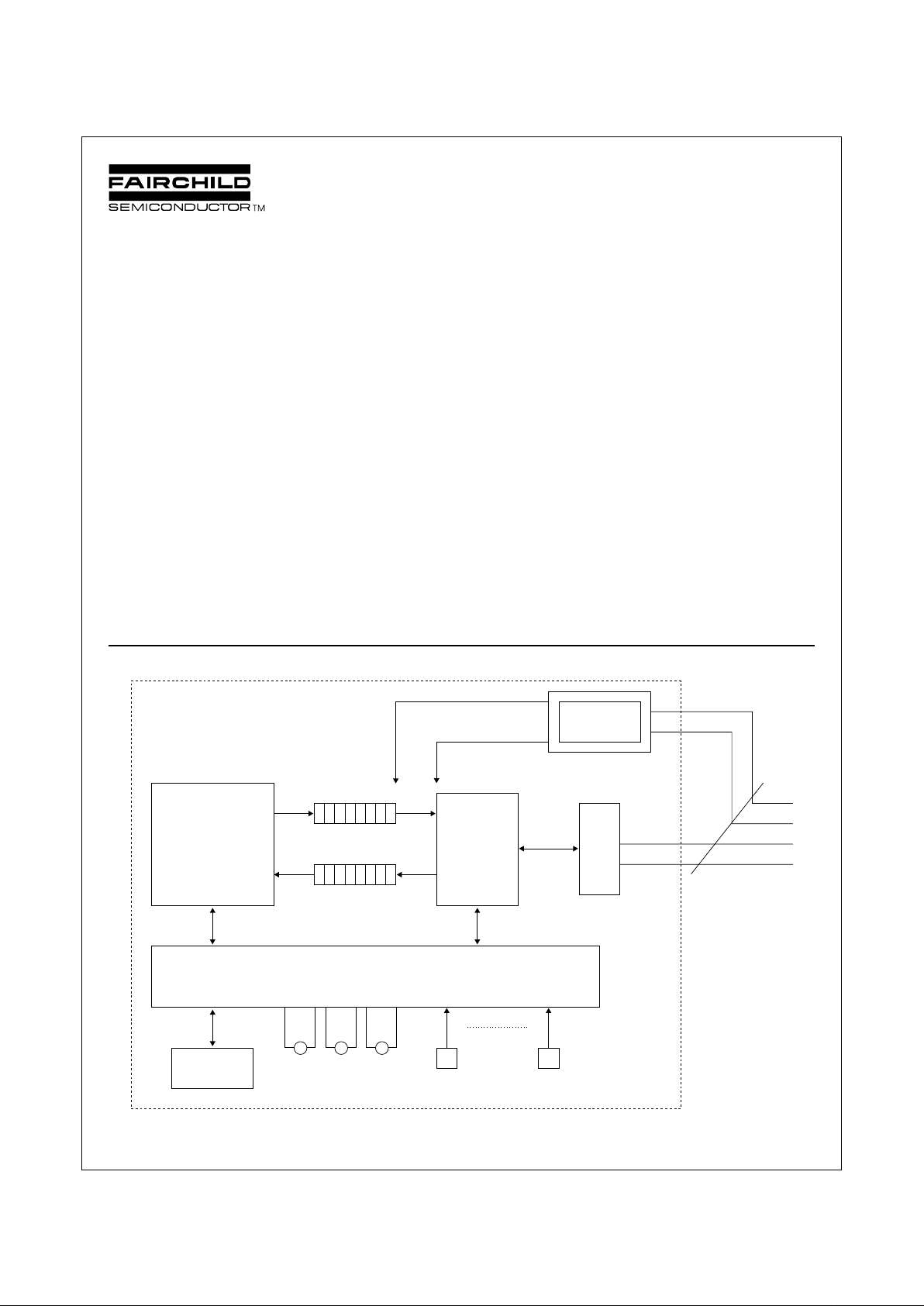
The USB100 is a Low cost, fully customizable controller for USB
HID-class pointing devices. It is in full compliance with REV 1.0
of the USB standard and implements the HID class specification
for mice, trackballs, joysticks and gamepads. This device interprets the commands specified in the HID class document and
provides appropriate responses from an On-Chip EEPROM. It
also provides ability to customize the device according to individual needs of the designers. Programming utilities supplied with
this device allow HID manufacturers to easily create the necessary data to be programmed into the device.
The device includes the necessary transceiver for USB operation
and meets all of the active and standby current specifications for
a bus-powered device.
Block Diagram
PRELIMINARY
January 1999
Features
■ USB 1.0 standard compliant
■ Has the necessary on-chip transceivers
■ Support for 2D and 3D mice with 2, 3 or more buttons
■ Supports 3 potentiometer mechanisms for joysticks
■ Up to 16 buttons for digital gamepads
■ Choice of 18-pin and 24-pin packages
■ Choice of 2Kbit and 4Kbit EEPROM densities
Use "A Diagram Number" Style Sheet"
STATE MACHINE
USB
COMMAND
PROCESSOR
(HID)
SERIAL
INTERFACE
ENGINE
X
C
V
R
POWER
EEPROM
TX-FIFO
RX-FIFO
USB CABLE
(D+, D-,
POWER &
GROUND)
UP TO 16 BUTTONS
UP TO 3 ROLLER/
POTENTIOMETER
MECHANISMS
© 1999 Fairchild Semiconductor Corporation
2
www.fairchildsemi.com
USB100 Programmable Low-Cost USB Machine (PLUM)
USB100 rev.D
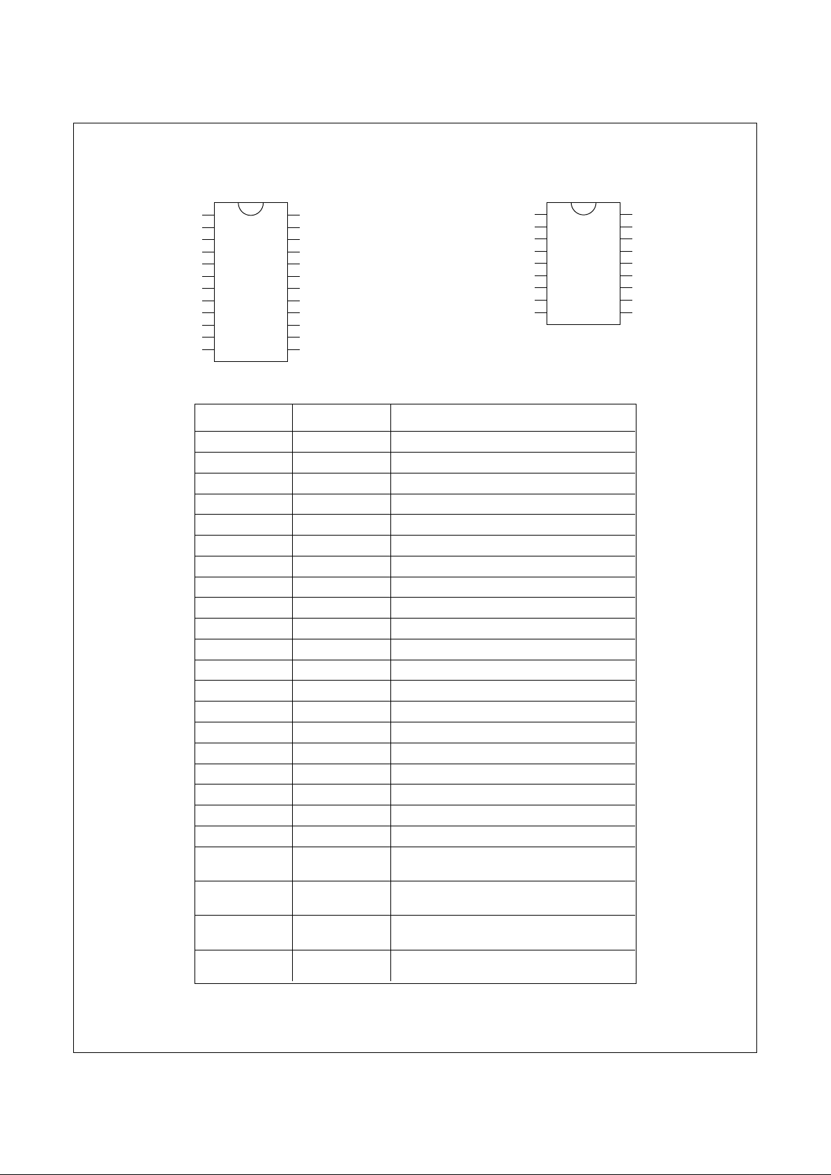
Pin Description
Pin Type Description
H4 I Roller/Button/Joystick input.
H3 I Roller/Button/Joystick input.
O2 I/O Register output pin / Button input.
OSC1 I Crystal input number 1.
OSC2 I Crystal input number 2
B4 I Button input
Reset I Active high reset pin
H1 I Roller/Button/Joystick input.
H2 I Roller/Button/Joystick input.
V1 I Roller/Button/Joystick input.
V2 I Roller/Button/Joystick input.
GND I Ground
B7 I Button input
B6 I Button input
B5 I Button input
VDD I Positive power supply
USBD+ O USB D + line
USBD- O USB D – line
GND I Ground
B8/F I/O Button input / LED driver
B1/CS I Button input and chip select to internal
EEPROM.*
B2/SK I Button input and system clock to internal
EEPROM.*
B3/DI I Button input and data in to internal
EEPROM.*
O1/DO O Button input and data out to read from
internal EEPROM.*
* See Programming internal EEPROM section
Pinout
24 Pin Package 18 Pin 3D Package
OSC1 VDD
OSC2 B6
H4 USBD+
B8/F USBD-
RESET GND
H3 B7
H1 B5
H2 B1
V1 B2
V2 B3
O2 B4
GND O1
OSC2 OSC1
H4 VDD
F USBD+
RESET USBD-
H3 GND
H1 B1
H2 B2
V1 B3
V2 O1
3
www.fairchildsemi.com
USB100 Programmable Low-Cost USB Machine (PLUM)
USB100 rev.D
Absolute Maximum Ratings
Ambient Storage Temperatures -65°C to + 150°C
All Input or Output Voltages with VCC + 1 to – 0.3V
respect to ground
Lead Temperature +300%
(Soldering, 10 seconds)
ESD Rating 2000V
Operating Conditions
Ambient Operating Temperature 0°C to +70°C
Power Supply (VCC) Range 4.4V to 5.5V
DC and AC Electrical Characteristics 4.4V ≤ VCC ≤ 5.5V
Symbol Parameter Conditions Min Max Units
I
CCA
Operating Current USB interface in active mode 40 mA
I
CCS
Standby Current USB interface in suspend 500 µA
V
IL
Input Low Voltage 0.8 V
V
IH
Input High Voltage 2 V
V
OL
Output Low Voltage 0.4 V
V
OH
Output High Voltage 2.4 V
I
IL
Input Leakage Current 2.5 µA
I
OL
Output Leakage Current 2.5 µA
F
SK
SK Clock Frequency Note 3 0 1 MHz
T
SKH
SK High Time 250 ns
T
SKL
SK Low Time 250 ns
T
CS
Minimum CS Low Time Note 4 250 ns
T
CSS
CS Setup Time 50 ns
T
DH
DO Hold Time 70 ns
T
DIS
DI Setup Time 100 ns
T
CSH
CS Hold Time 0 ns
T
DIH
DI Hold Time 20 ns
T
PD1
Output Delay to “1” 500 ns
T
PD0
Output Delay to “0” 500 ns
T
SY
CS to Status Valid 500 ns
T
DF
CS to DO in TRI-STATE 100 ns
T
WP
Write Cycle Time 10 ms
AC Test Conditions
Output Load 1 TTL Gate
Input Pulse Levels 0.4V and 2.4V
Timing Measurements Reference Level
Input 1V and 2V
Output 0.8V and 2.0V
Note 1: Stress ratings above those listed under “Absolute Maximum Ratings” may cause permanent damage to the device. This is a stress rating only and operation of the
device at these or any other conditions above those indicated in the operational sections of the specification is not implied. Exposure to absolute maximum rating conditions for
extended periods may affect device reliability.
Note 2: The shortest allowable S clock period = 1/fSK (as shown under the fSK parameter). Maximum SK clock speed (minimum SK period) is determined by the interaction of
several AC parameters stated in the datasheet. Within this SK period, both t
SKH
and t
SKL
limits must be observed. Therefore, it is not allowable to set 1/fSK = t
SKH
(minimum) +
t
SKL
(minimum) for shorter SK cycle time operation.
Note 3: CS (Chip Select) must be brought low (to VIL) for an interval of tCS in order to reset all internal device registers (device reset) prior to beginning another opcode cycle.
(This is shown in the opcode diagrams in the following pages.)
 Loading...