Fairchild Semiconductor UC3845D1, UC3843D1, UC3844D1, UC3845, UC3844 Datasheet
...
www.fairchildsemi.com
UC3842/UC3843/UC3844/UC3845
SMPS Controller
Features
• Low Start up Current
• Maximum Duty Clamp
• UVLO With Hysteresis
• Operating Fr equency up to 500KHz
Description
The UC3842/UC3843/UC3844/UC3845 are fixed
frequencycurrent-mode PWM controller. They are specially
designed for Off-Line and D C t o DC con ver t e r a pp l ic ati o ns
with minimum external components. These integrated
circuits feature a trimmed oscillator for precise duty cycle
control, a temperature compensated reference, high gain
error amplifier, current sensing comparator and a high
current totemp ole ou t pu t for dr ivi n g a Po we r M OSF E T. The
UC3842 and UC3844 have UVLO threshold s of 16V (on)
and 10V (off ). The UC3843 and UC3845 are 8.5V(on) and
7.9V (off). The UC3842 and UC3843 can operate within
100% duty cycle. The UC3844 and UC3845 can operate
with 50% duty cycle.
8-DIP
14-SOP
8-SOP
1
1
1
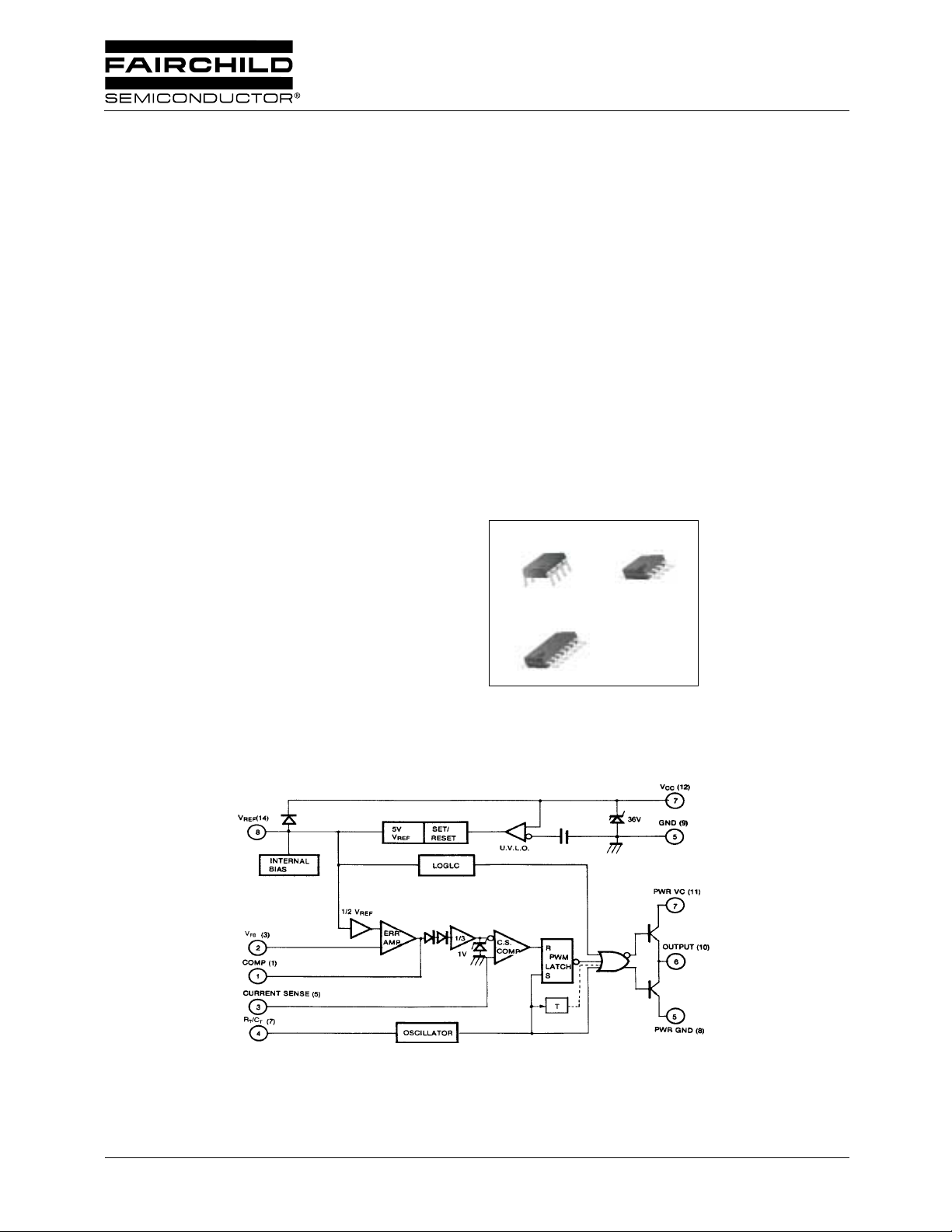
Internal Block Diagram
* NORMALLY 8DIP/8SOP PIN NO.
* ( ) IS 14SOP PINNO.
* TOGGLE FLIP FLOP USED ONLY IN UC3844, UC3845
©2002 Fairchild Semiconductor Corporation
Rev. 1.0.1

UC3842/UC3843/UC3844/UC3845
Absolute Maximum Ratings
Parameter Symbol Value Unit
Supply Voltage V
Output Current I
Analog Inputs (Pin 2.3) V
Error Amp Output Sink Current I
Power Dissipation at T
Power Dissipation at T
Power Dissipation at T
≤25°C (8DIP) P
A
≤25°C (8SOP) P
A
≤25°C (14SOP) P
A
Storage Temperature Range T
Lead Temperature (Soldering, 10sec) T
CC
O
(ANA)
SINK (E.A)
(Note1,2) 1200 mW
D
(Note1,2) 460 mW
D
(Note1,2) 680 mW
D
STG
LEAD
Note:
1. Board Thickness 1.6mm, Board Dimension 76.2mm ×114.3mm, (Reference EIA / JS ED51-3, 51-7)
2. Do not exceeed P
and SOA (Safe Operation Area)
D
30 V
±1A
-0.3 to 6.3 V
10 mA
-65 ~ +150 °C
+300 °C
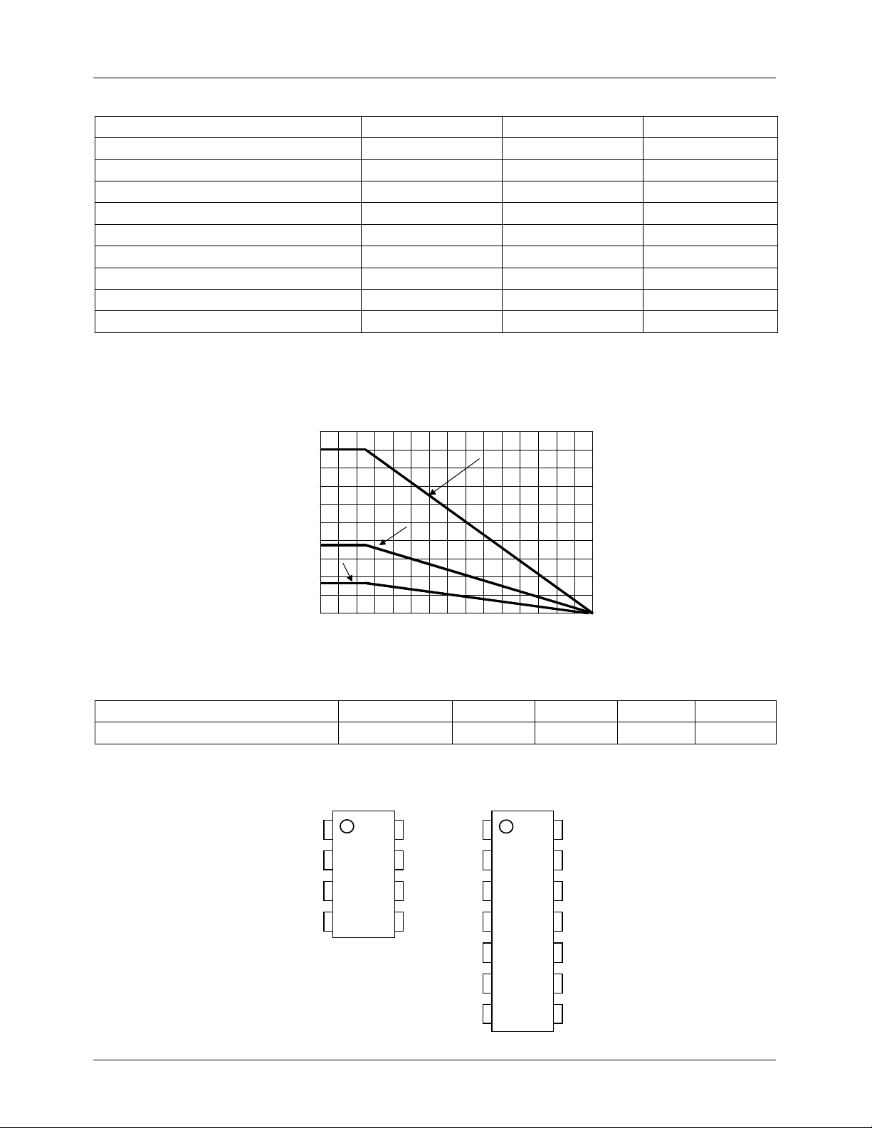
Power Dissipation Curve
1200
1200
1100
1100
1000
1000
900
900
14SOP
800
800
700
700
8SOP
8SOP
600
600
500
500
POWER DISSIPATION (mW)
POWER DISSIPATION (mW)
400
400
300
300
0 102030405060708090100110120130140150
0 102030405030 40 50 60 70 8060 70 80 90 100 11090 100 110 120 130 140120 130 140 150
14SOP
AMBIENT TEMPERATURE (℃)
AMBIENT TEMPERATURE (℃)
8DIP
8DIP
Thermal Data
Characteristic Symbol 8-DIP 8-SOP 14-SOP Unit
Thermal Resistance Junction-ambient R
thj-amb(MAX)
100 265 180 °C/W
Pin Array
8DIP,8SOP
8DIP,8SOP
REF
REF
REF
V
V
V
8
8
COMP
COMP
COMP
CURRENT SENSE
CURRENT SENSE
CURRENT SENSE
RT/C
RT/C
RT/C
1
1
1
FB
FB
FB
V
V
V
2
2
2
3
3
3
T
T
T
4
4
4
8
7
7
7
6
6
6
5
5
5
CC
CC
CC
V
V
V
OUTPUT
OUTPUT
OUTPUT
GND
GND
GND
COMP
COMP
COMP
CURRENT SENSE 5
CURRENT SENSE 5
CURRENT SENSE 5
2
N/C 2
N/C 2
N/C 2
N/C
N/C
N/C
N/C
N/C
N/C
T/CT
T/CT
T/CT
R
R
R
14SOP
14SOP
14
14
14
REF
REF
13
13
13
12
12
12
11
11
11
10
10
10
9
9
9
8
8
8
REF
V
V
V
N/C
N/C
N/C
CC
CC
CC
V
V
V
PWR V
PWR V
PWR V
OUTPUT
OUTPUT
OUTPUT
GND
GND
GND
PWR GND
PWR GND
PWR GND
C
C
C
1
1
1
FB
FB
FB
V
V
V
3
3
3
4
4
4
6
6
6
7
7
7

UC3842/UC3843/UC3844/UC3845
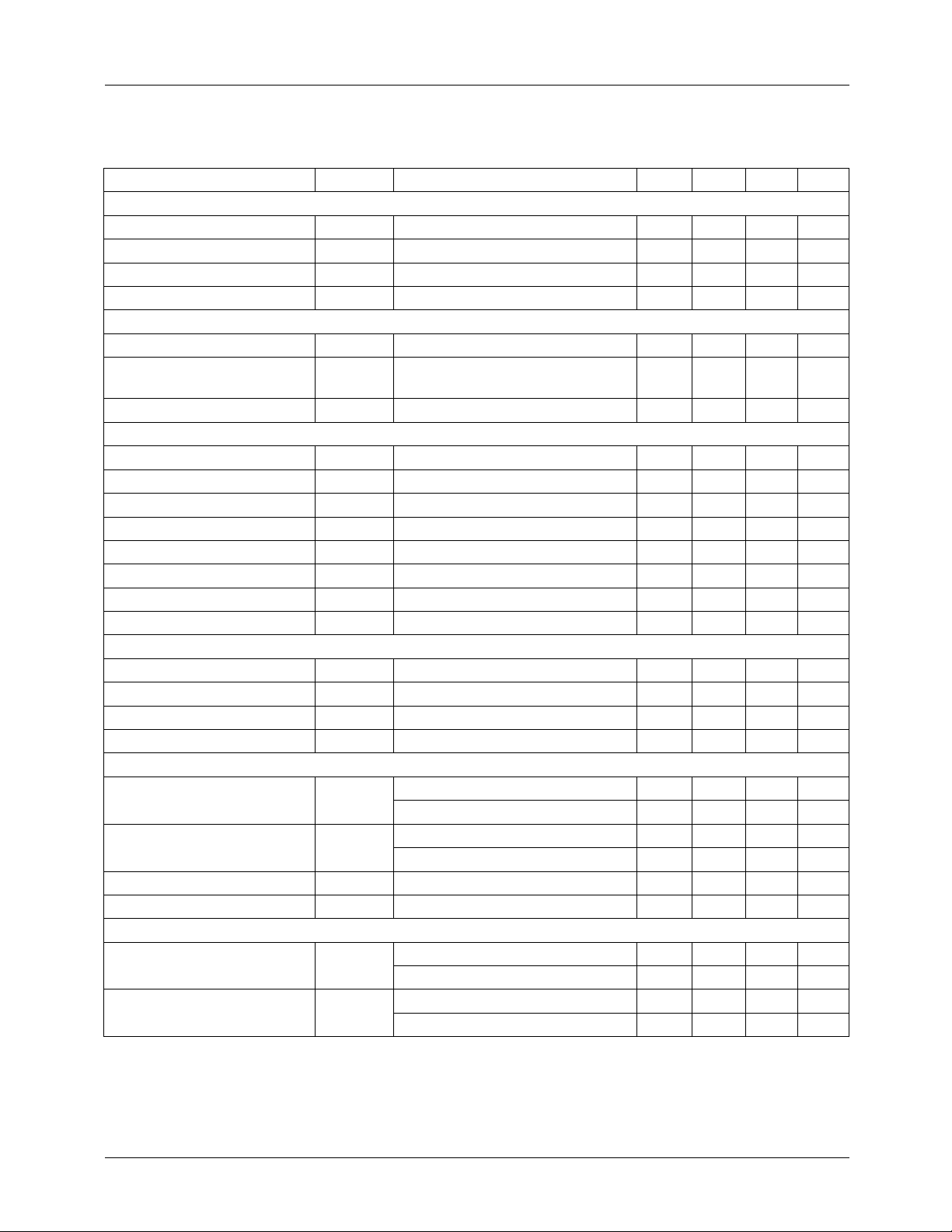
Electrical Characteristics
(VCC=15V, RT=10kΩ, CT=3.3nF, TA= 0°C to +70°C, unless otherwise specified)
Parameter Symbol Conditions Min. Typ. Max. Unit
REFERENCE SECTION
Reference Output Voltage V
Line Regulation ∆V
Load Regulation ∆V
Short Circuit Output Current I
REF
REF
REF
SC
OSCILLATOR SECTION
Oscillation Frequency f T
Frequency Change with
Voltage
Oscillator Amplitude V
∆f/∆V
OSC
ERROR AMPLIFIER SECTION
Input Bias Current I
Input Voltage V
Open Loop Voltage Gain G
BIAS
I(E>A)
VO
Power Supply Rejection Ratio PSRR 12V ≤ V
Output Sink Current I
Output Source Current I
High Output Voltage V
Low Output Voltage V
SINK
SOURCE
OH
OL
CURRENT SENSE SECTION
Gain G
Maximum Input Signal V
I(MAX)
Power Supply Rejection Ratio PSRR 12V ≤ V
Input Bias Current I
BIAS
OUTPUT SECTION
V
Low Output Voltage
High Output Voltage
Rise Time t
Fall Time t
OL
V
OH
R
F
UNDER-VOLTAGE LOCKOUT SECTION
Start Threshold
Min. Operating Voltage
(After Turn On)
V
TH(ST)
V
OPR(MIN)
TJ = 25°C, I
12V ≤ V
1mA ≤ I
CC
REF
= 1mA 4.90 5.00 5.10 V
REF
≤ 25V - 6 20 mV
≤ 20mA - 6 25 mV
TA = 25°C - -100 -180 mA
= 25°C475257kHz
J
CC
12V ≤ V
≤ 25V - 0.05 1 %
CC
- -1.6-V
- --0.1-2µA
V
= 2.5V 2.42 2.50 2.58 V
pin1
2V ≤ V
V
pin2
V
pin2
V
pin2
V
pin2
(Note 1 & 2) 2.85 3 3.15 V/V
V
V
pin1
≤ 4V (Note3) 65 90 - dB
O
≤ 25V (Note3) 60 70 - dB
CC
= 2.7V, V
= 2.3V, V
= 1.1V 2 7 - mA
pin1
= 5V -0.6 -1.0 - mA
pin1
= 2.3V, RL = 15kΩ to GND 5 6 - V
= 2.7V, RL = 15kΩ to Pin 8 - 0.8 1.1 V
= 5V(Note 1) 0.9 1 1.1 V
≤ 25V (Note 1,3) - 70 - dB
CC
- --3-10µA
I
= 20mA - 0.08 0.4 V
SINK
= 200mA - 1.4 2.2 V
I
SINK
I
SOURCE
I
SOURCE
= 20mA 13 13.5 - V
= 200mA 12 13.0 - V
TJ = 25°C, CL= 1nF (Note 3) - 45 150 ns
TJ = 25°C, CL= 1nF (Note 3) - 35 150 ns
UC3842/UC3844 14.5 16.0 17.5 V
UC3843/UC3845 7.8 8.4 9.0 V
UC3842/UC3844 8.5 10.0 11.5 V
UC3843/UC3844 7.0 7.6 8.2 V
P-P
3

UC3842/UC3843/UC3844/UC3845
Electrical Characteristics
(Continued)
(VCC=15V, RT=10kΩ, CT=3.3nF, TA= 0°C to +70°C, unless otherwise specified)
Parameter Symbol Conditions Min. Typ. Max. Unit
PWM SECTION
Max. Duty Cycle
Min. Duty Cycle D
D
D
(Max)
(Max)
(MIN)
UC3842/UC3843 95 97 100 %
UC3844/UC3845 47 48 50 %
- --0%
TOTAL STANDBY CURRENT
Start-Up Current I
Operating Supply Current I
Zener Voltage V
Adjust V
Note:
1. Parameter measured at trip point of latch
2. Gain defined as:
A
3. These parameters, although guaranteed, are not 100 tested in production.
above the start threshould before setting at 15V
CC
∆V
pin1
----------------- -=
∆V
pin3
,0 ≤ V
pin3
≤ 0.8V
ST
CC(OPR)
Z
V
pin3=Vpin2
ICC = 25mA 30 38 - V
- -0.451mA
=ON - 14 17 mA
UC3842
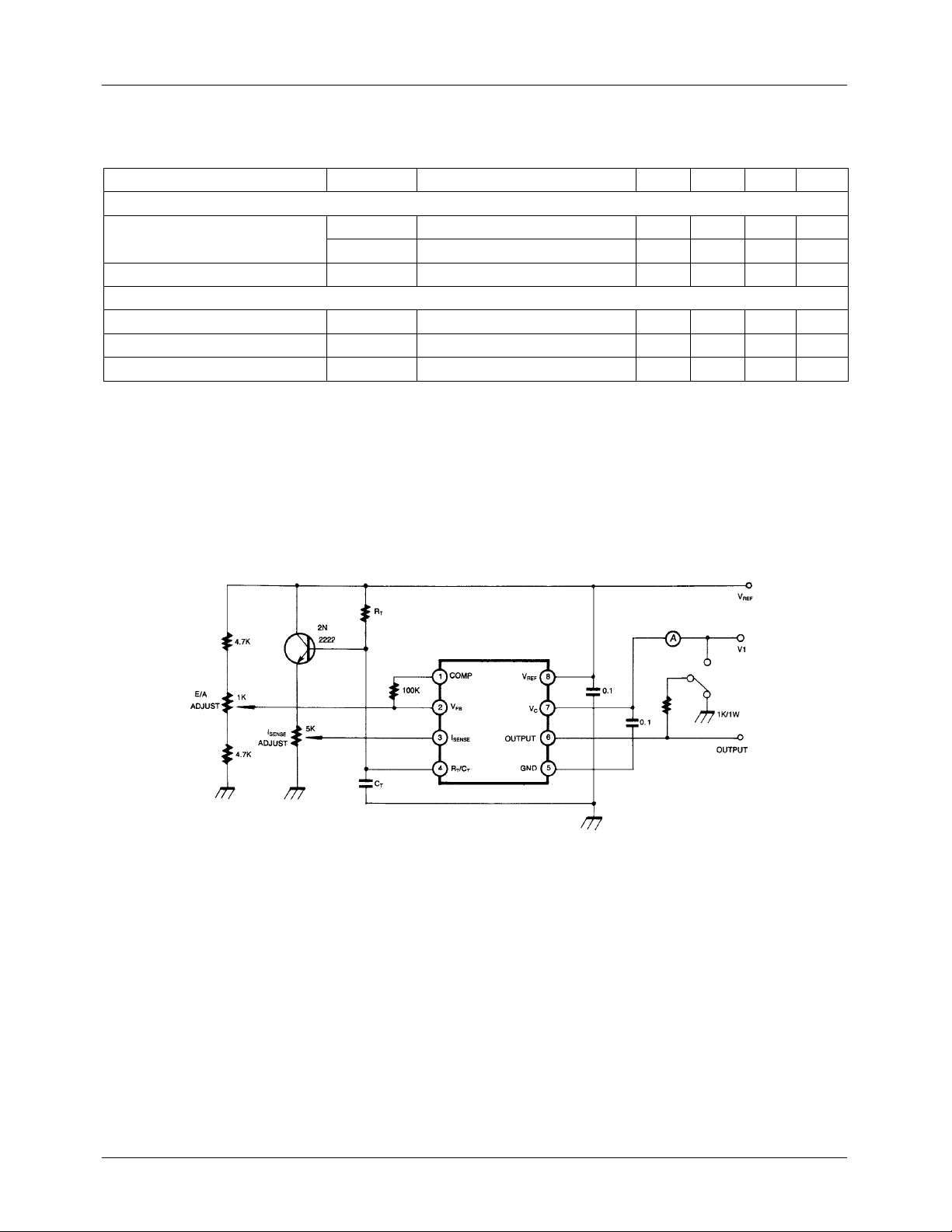
Figure 1. Open Loop Test Circuit
High peak currents associated with capacitive loads necessitate careful grounding techniques Timing and bypass capacitors
should be c onnected close to pin 5 in a single point ground. The transistor and 5kΩ potentiometer are used to sample the
oscillator waveform and apply an adjustable ramp to pin 3.
4
 Loading...