Fairchild Semiconductor UC3843A, UC3842A Datasheet

UC3842A/UC3843A
SMPS Controller
www.fairchildsemi.com
Features
• Low Start Current 0.2mA (typ)
• Operating R ange Up To 500KHz
• Cycle by Cycle Current Limiting
• Under Voltage Lock Out With Hysteresis
• Short Shutdown Delay Time: typ.100ns
• High Current Totem-pole Output
• Output Swing Lim i ti ng: 22 V
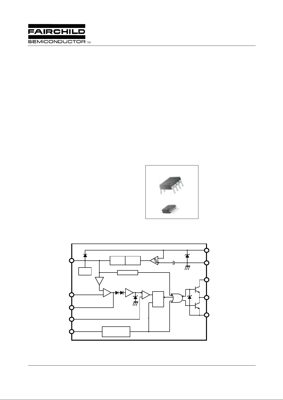
Internal Block Diagram
Description
The UC3842A/UC 38 43A ar e fixe d P WM co ntrol ler for O f fLine and DC to DC converter applications. The internal circuits include UVLO, low start up current circuit, temperature compensated reference, high gain error amplifier,
current sensing comp a ra to r, and high current totem-pole output for driving a POWER MOSFET. Also UC3842A/
UC3843A provide low start up current below 0.3mA and
short shutdown delay time typ. 100ns. The UC3842A has
UVLO thresho ld o f 16V (on ) an d 10V (of f ). Th e U C3843 A i s
8.4V(on) and 7.6V(off). The UC3842A and UC3843A c an
operate within 100% duty cycle.
8-DIP
1
8-SOP
1
8
REF
V
Internal
Bias
1/2V
REF
2
FB
V
1
COMP
3
C.S
T/CT
R
4
©2000 Fairchild Semiconductor International
5V
V
Error Amp
+
-
OSCILLATOR
RESET
REF
Good LOGIC
1/3
SET/
1V
C.S
Comp.
UVLO
PWM
LATCH
R
S
T
29V
22V
7
V
5
GND
PWR
7
V
6
OUTPUT
PWR
5
GND
CC
C
Rev. 5.0

UC3842A/UC3843A
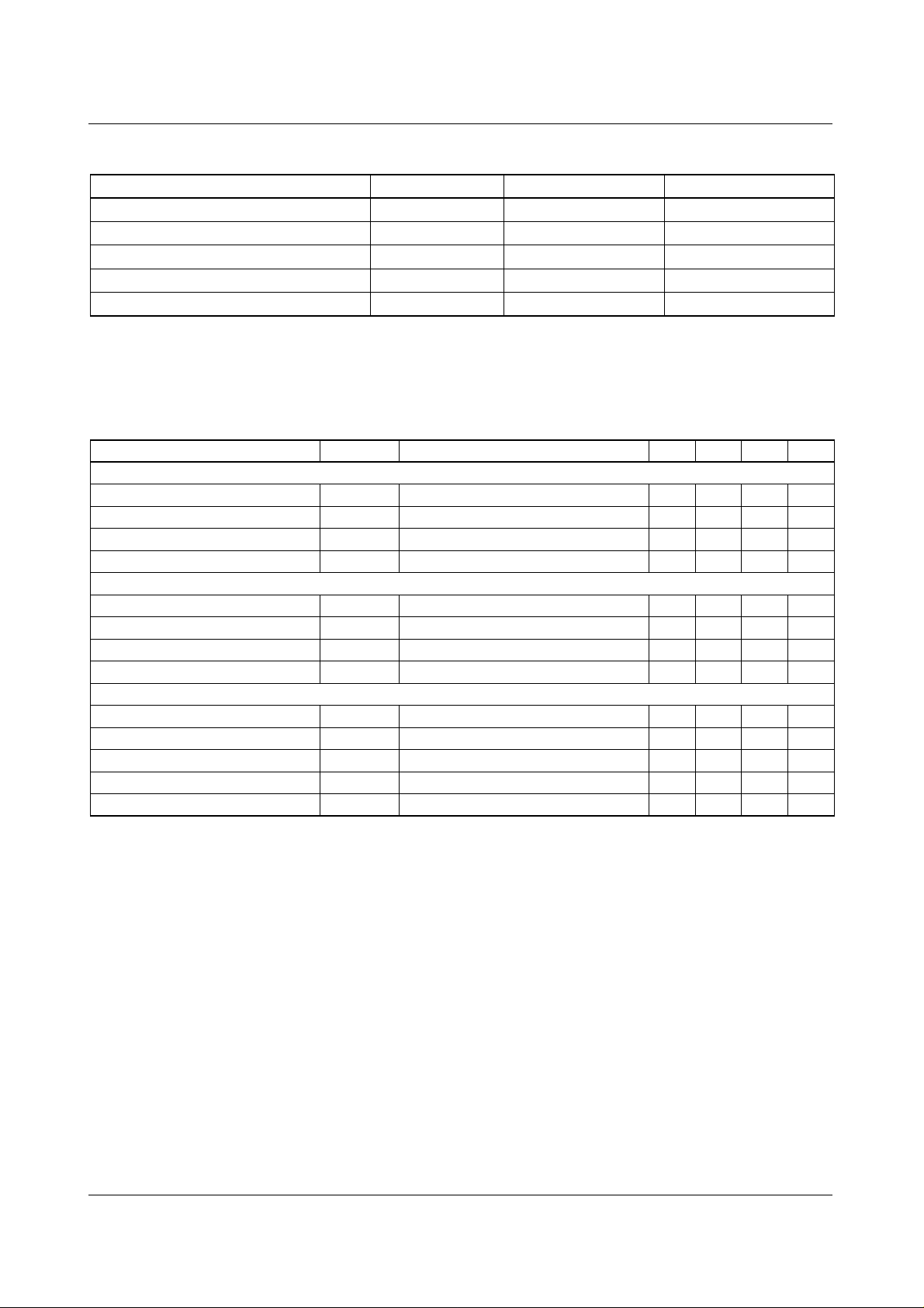
Absolute Maximum Ratings
Parameter Symbol Value Unit
Supply Voltage V
Output Current I
Analog Inputs (pin 2, 3) V
Error Amp. Output Sink Current I
I(ANA)
SINK(EA)
Power Dissipation P
CC
O
D
30 V
± 1 A
- 0.3 to 6.3 V
10 mA
1W
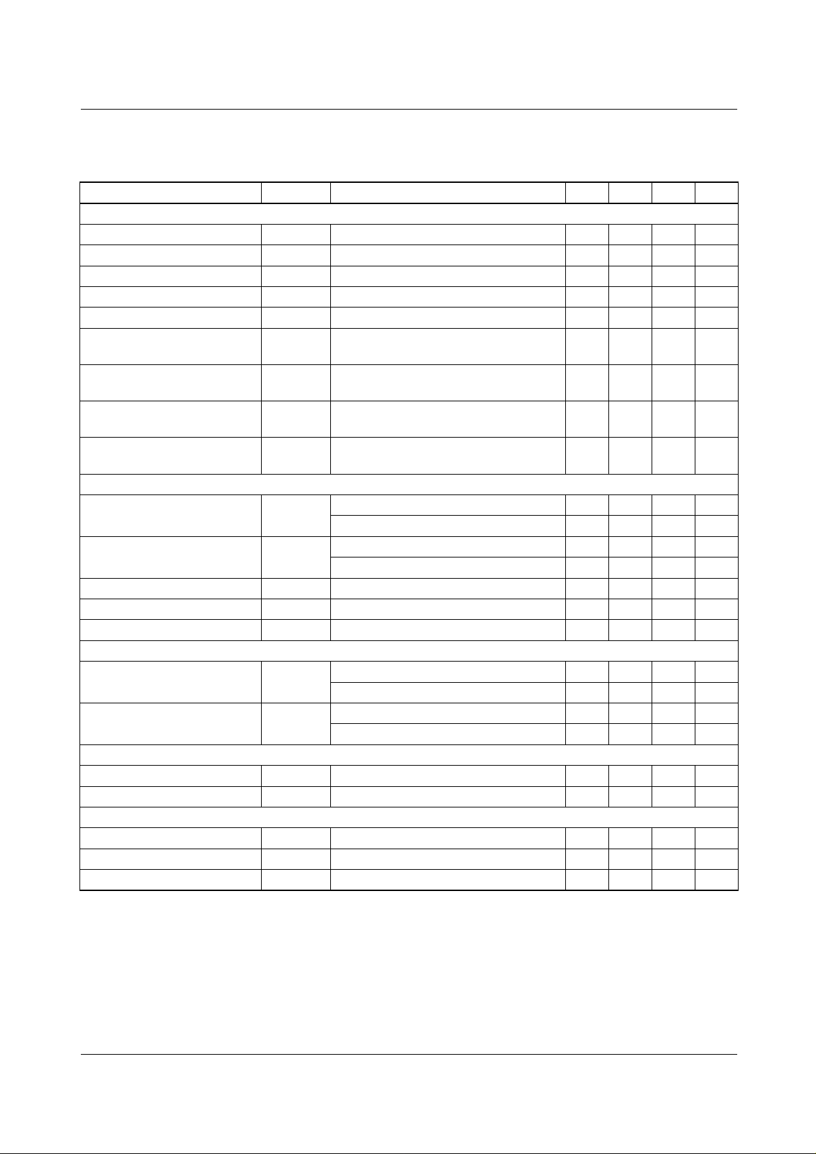
Electrical Characteristics
(VCC = 15V, RT = 10KΩ, CT = 3.3nF, TA = 0°C to + 70°C ,Unless otherwise specified)
Parameter Symbol Conditions Min. Typ. Max. Unit
REFERENCE SECTION
Output Voltage V
Line Regulation ∆V
Load Regulation ∆V
Output Short Circuit I
REF
REF
REF
SC
OSILLATOR SECTION
Initial Accuracy F
OSC
Voltage Stability ST
Amplitude V
Discharge Current I
OSC
DISCHG
CURRENT SENSE SECTION
Gain G
Maximum Input Signal V
I(MAX)
PSRR PSRR V
Input Bias Current I
Delay to Output T
BIAS
D
TJ = 25°C, IO = 1mA 4.9 5.0 5.1 V
VCC = 12V to 25V - 6 20 mV
IO = 1mA to 20mA - 6 25 mV
Ta = 25°C - - 100 - 180 mA
TJ = 25°C 47 52 57 KHz
V
V
= 12V to 25V - 0.2 1 %
CC
V
, Peak to Peak - 1.7 - V
PIN4
TJ = 25°C, Pin4 = 2V 7.8 8.3 8.8 mA
(NOTE 2, 3) 2.85 3 3.15 V/V
V
V
= 5V(NOTE 2) 0.9 1.0 1.1 V
PIN1
= 12V to 25V (NOTE 1, 2) - 70 - dB
CC
- - - 2 -10 uA
V
= 0 V to 2V (NOTE1) - 100 200 ns
PIN3
2

Electrical Characteristics (Continued)
(VCC = 15V, RT = 10KΩ, CT = 3.3nF, TA = 0°C to + 70°C, Unless otherwise specified)
Parameter Symbol Conditions Min. Typ. Max. Unit
ERROR AMPLIFIER SECTION
Input Voltage V
Input Bias Current I
Open Loop Gain G
BIAS
VO
Unity Gain Bandwidth GBW T
PSRR PSRR V
Output Sink Current I
Output Source Current I
Output High Voltage V
Output Low Voltage V
SINK
SOURCE
OH
OL
OUTPUT SECTION
Output Low Level V
Output High Level V
Rise Time t
Fall Time t
Output Voltage Swing Limit V
OL
OH
R
F
OLIM
UNDER VOLTAGE LOCKOUT SECTION
Start Threshold V
Min. Operating Voltage
( After turn on )
TH
V
TL
PWM SECTION
Maximum Duty Cycle D
Minimum Duty Cycle D
MAX
MIN
TOTAL STANDBY CURRENT
Start-Up Current I
Operating Supply Current I
Zener Voltage V
V
CC
ST
CC
Z
T
I
= 2.5V 2.42 2.50 2.58 V
PIN1
- - -0.3 - 2 uA
VO = 2V to 4V (NOTE 1) 65 90 - dB
= 25°C (NOTE 1) 0.7 1 - MHz
J
= 12V to 25V (NOTE 1) 60 70 - dB
CC
V
= 2.7V
PIN2
V
= 1.1V
PIN1
V
= 2.3V
PIN2
V
= 5.0V
PIN1
V
= 2.3V
PIN2
R1 = 15KΩ to GND
V
= 2.7V
PIN2
R1 = 15KΩ to Pin8
I
= 20mA - 0.1 0.4 V
SINK
I
= 200mA - 1.5 2.2 V
SINK
I
SOURCE
I
SOURCE
= 20mA 13 13.5 - V
= 200mA 12 13.5 - V
TJ = 25°C, C1 = 1nF (NOTE 1) - 40 100 ns
TJ = 25°C, C1 = 1nF (NOTE 1) - 40 100 ns
VCC = 27V, C1 = 1nF - 22 - V
UC3842A 15 16 17 V
UC3843A 7.8 8.4 9.0 V
UC3842A 9 10 11 V
UC3843A 7.0 7.6 8.2 V
UC3842A/UC3843A 94 96 100 %
- --0%
- -0.20.4mA
V
PIN2
= V
= 0V - 11 17 mA
PIN3
ICC = 25mA - 29 - V
UC3842A/UC3843A
26-mA
-0.5 -0.8 - mA
56-V
-0.81.1V
* Adjust VCC above the start threshold before setting at 15V
Notes :
1. These parameters, although guaranteed, are not 100% tested in production.
2. Parameter measured at trip point of latch with V2 = 0V.
3. Gain define d as: G
= ∆V
V
PIN1∆VPIN3(VPIN3
= 0 to 0.8V)
3
 Loading...