

Fairchild Semiconductor TN6727A Datasheet
TN6727A
TN6727A
PNP General Purpose Amplifier
This device is designed for general purpose medium power amplifiers and switches requiring collector currents to
Absolute Maximum Ratings* T
V
V
V
I
C
T
*These ratings are limiting values above which the serviceability of any semiconductor device may be impaired.
NOTES:
1) These ratings are based on a maximum junction temperature of 150°C.
2) These are steady state limits. The factory should be consulted on applications involving pulsed or low duty cycle operations.
Thermal Characteristics T
P
R
R
C
B
E
1A. Sourced from Process 77. See TN6726A for characteristics.
ParameterSymbol
CES
CBO
EBO
J, Tstg
Symbol
D
θJC
θJA
Total Device Dissipation
Derate above 25°C
TO-226
A = 25°C unless otherwise noted
A = 25°C unless otherwise noted
Characteristic
Value
Max
TN6727A
1
8
Units
V40Collector-Emitter Voltage
V50Collector-Base Voltage
V5Emitter-Base Voltage
A1.5Collector Current - Continuous
°C-55 to +150Operating and Storage Junction Temperature Range
Units
W
mW/°C
°C/W50Thermal Resistance, Junction to Case
°C/W125Thermal Resistance, Junction to Ambient
1997 Fairchild Semiconductor Corporation
Page 1 of 2
SMALL SIGNAL CHARACTERISTICS
OFF CHARACTERISTICS
PNP General Purpose Amplifier
TN6727A
(continued)
Electrical Characteristics T
BV
CEO
BV
CBO
BV
EBO
I
CBO
I
EBO
ON CHARACTERISTICS*
h
FE
V
CE(sat)
V
BE(on)
Collector-Emitter Breakdown Voltage
Collector-Base Breakdown Voltage
Emitter-Base Breakdown Voltage
Collector Cutoff Current
Emitter Cutoff Current
DC Current Gain
Collector-Emitter Saturation Voltage
Base-Emitter On Voltage
A = 25°C unless otherwise noted
IC = 10 mA
IC = 1 mA
IE = 1 mA
VCB = 50 V
VEB = 5 V
IC = 10 mA, VCE = 1 V
IC = 100 mA, VCE = 1 V
IC = 1A, VCE = 1 V
IC = 1 A, IB = 100 mA
IC = 1 A, VCE = 1 V
55
60
50
UnitsMaxMinTest ConditionsParameterSymbol
V40
V50
V5
nA100
nA100
-
250
V0.5
V1.2
*Pulse Test: Pulse Width ≤ 300 µs, Duty Cycle ≤ 1.0%
C
cb
h
fe
Output Capacitance
Small Signal Current Gain
VCB = 10 V, IE = 0, f = 1MHz
IC = 50 mA,VCE = 10 V, f=20MHz
pF30
-252.5
Page 2 of 2
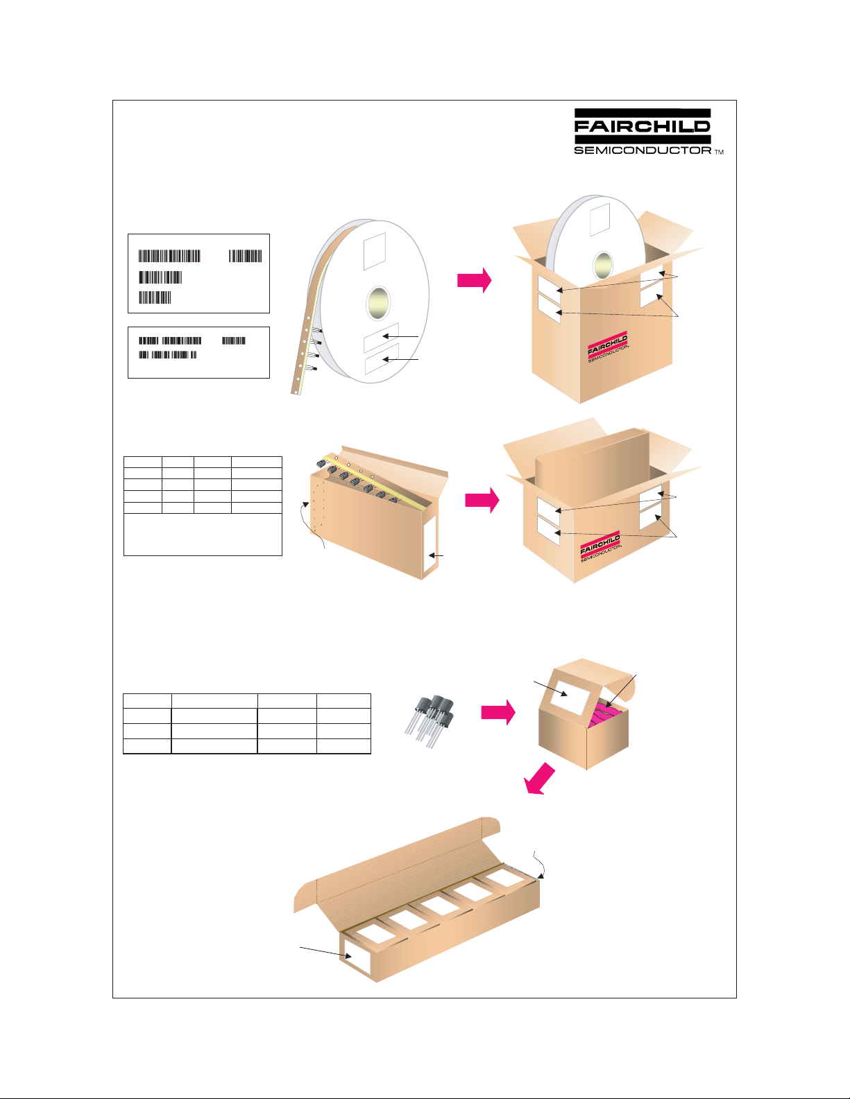
TO-226AE Tape and Reel Data and Package Dimensions
TO -226AE Packaging
Co nfigu ratio n: Figur e 1.0
FSCINT Label sample
FAIRCHILD SEMICONDUCTOR CORPORAT ION
LOT:
CBVK741B019
NSID:
PN2222N
D/C1:
SPEC REV:
D9842
QA REV:
HTB:B
QTY:
10000
SPEC:
B2
(FSCINT)
F63TNR Label s ample
LOT: CBVK7 41B019
FSID: PN222N
D/C1: D9842 QTY1: SPEC REV:
D/C2: QTY2: CPN:
QTY: 2000
SPEC:
N/F: F (F63TNR)3
TO-226AE TNR/AMMO PACKING INF ROMATION
Packing Styl e Quantity EOL code
Reel A 2,000 D26Z
Amm o M 2,000 D74Z
Unit w eig ht = 0.300gm
Reel weight with com ponents = 0.868 kg
Ammo weight wi th compon ents = 0.880 kg
Max quanti ty per in termediate bo x = 10,000 uni ts
E2,000 D27Z
P2,000 D75Z
(TO-226AE ) BULK PACKING INFORMATION
EOL CODE DESCRIPTION
TO-18 OPTION STD NO LEAD CLIP
J18Z
TO-5 OPTION STD NO LEAD CLIP
J05Z
CODE
TO-226 STANDARD
STRAIGHT
NO EOL
LEADCLIP
DIMENSION
NO LEADCL IP
327mm x 158mm x 135mm
Immed iate Bo x
Cus tom ized
Labe l
QUANTITY
1.0 K / BOX
1.0 K / BOX
1.5 K / BOX
TAPE and REEL OPTION
See Fig 2.0 for various
Reeling Styles
5 Reels per
Int ermed iate Bo x
F63TNR
Labe l
Cus tom ized
Labe l
AMMO PACK OPTION
See Fig 3.0 for 2 Ammo
Pack Options
5 Am mo box es per
Int ermed iate Bo x
F63TNR
Bar code Label
BULK OPTION
See Bulk Packing
Information table
FSCINT Bar code Label
1,500 un its per
EO70 box for
st d option
375mm x 267mm x 375mm
Int ermed iate Bo x
333mm x 231mm x 183mm
Int ermed iate Bo x
Anti-stat ic
Bub ble Sheets
114mm x 102mm x 51mm
EO70 Immedi ate Box
FSCINT
Labe l
Cus tom ized
Labe l
FSCINT
Labe l
Cus tom ized
Labe l
530mm x 130mm x 83mm
Intermediate box
FSCINT Labe l
Cus tomized
Label
7,500 un its m aximu m
per intermedi ate box
for std opt ion
5 EO70 boxes per
Int ermed iate Bo x
October 1999, Rev. A1
 Loading...