Fairchild Semiconductor TN6716A Datasheet

TN6716A
TN6716A
C
B
E
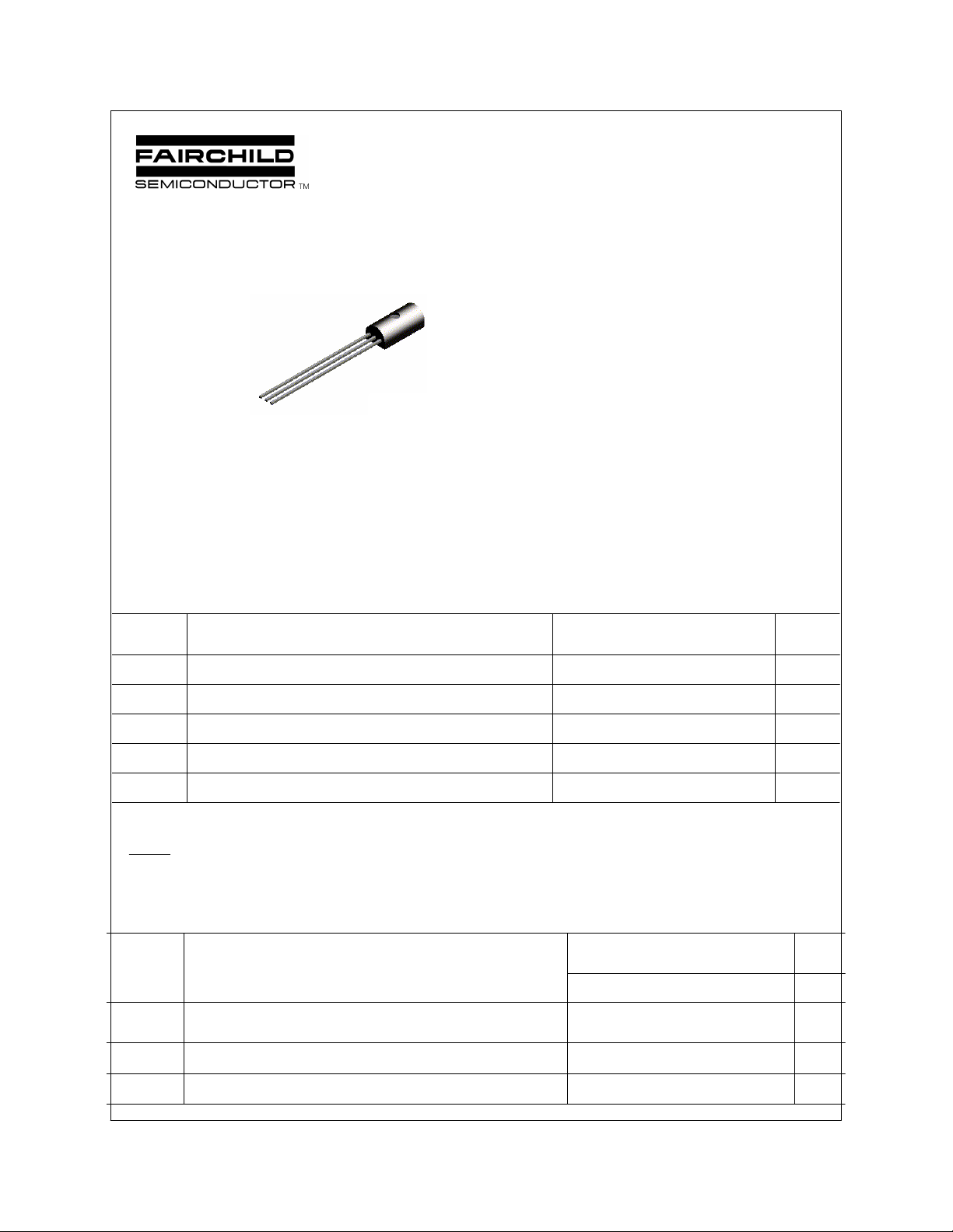
TO-226
NPN General Purpose Amplifier
This device is designed for general purpose medium power amplifiers and switches requiring collector currents to
1.2A. Sourced from Process 38. See TN6715A for characteristics.
Absolute Maximum Ratings* T
ParameterSymbol
V
CEO
V
CBO
V
EBO
I
C
T
J, Tstg
*These ratings are limiting values above which the serviceability of any semiconductor device may be impaired.
NOTES:
1) These ratings are based on a maximum junction temperature of 150°C.
2) These are steady state limits. The factory should be consulted on applications involving pulsed or low duty cycle operations.
A = 25°C unless otherwise noted
Value
Units
V60Collector-Emitter Voltage
V60Collector-Base Voltage
V5Emitter-Base Voltage
A2Collector Current - Continuous
°C-55 to +150Operating and Storage Junction Temperature Range
Thermal Characteristics T
Symbol
P
D
R
θJC
R
θJA
1997 Fairchild Semiconductor
Characteristic
Total Device Dissipation
Derate above 25°C
A = 25°C unless otherwise noted
Max
TA=25°C
1
8
Units
W
mW/°C
°C/W50Thermal Resistance, Junction to Case
°C/W125Thermal Resistance, Junction to Ambient
Pr38 TN6716A.SAM revC

SMALL SIGNAL CHARACTERISTICS
OFF CHARACTERISTICS
NPN General Purpose Amplifier
TN6716A
(continued)
Electrical Characteristics T
BV
CEO
BV
CBO
BV
EBO
I
CBO
I
EBO
ON CHARACTERISTICS
h
FE
V
CE(sat)
V
BE(on)
Collector-Emitter Breakdown Voltage
Collector-Base Breakdown Voltage
Emitter-Base Breakdown Voltage
Collector Cutoff Current
Emitter Cutoff Current
DC Current Gain
Collector-Emitter Saturation Voltage
Base-Emitter On Voltage
A = 25°C unless otherwise noted
IC = 1 mA
IC = 100 µA
IE = 1 mA
VCB = 40 V
VEB = 5 V
IC = 50 mA, VCE = 1 V
IC = 250 mA, VCE = 1 V
IC = 500 mA, VCE = 1 V
IC = 250 mA, IB = 10 mA
IC = 250 mA, IB = 25 mA
IC = 250 mA, VCE = 1.0 V
80
50
20
UnitsMaxMinTest ConditionsParameterSymbol
V60
V60
V5
nA100
uA10
-
250
V0.5
0.35
V1.2
C
*Pulse Test: Pulse Width ≤ 300 µs, Duty Cycle ≤ 1.0%
cb
Output Capacitance
Small Signal Current Gainhfe
VCB = 10 V, IE = 0, f = 1MHz
IC = 200 mA,VCE = 5 V,f=20MHz
pF30
MHz252.5
1997 Fairchild Semiconductor
Pr38 TN6716A.SAM revC

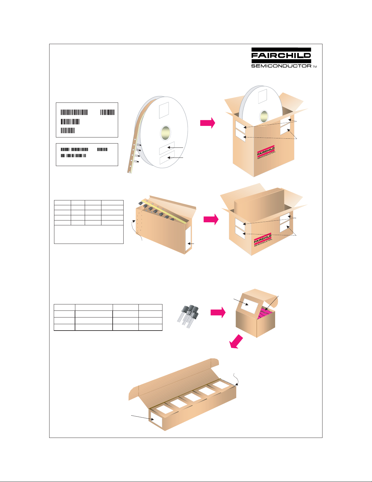
TO-226AE Tape and Reel Data and Package Dimensions
TO -226AE Packaging
Co nfigu ratio n: Figur e 1.0
FSCINT Label sample
FAIRCHILD SEMICONDUCTOR CORPORAT ION
LOT:
CBVK741B019
NSID:
PN2222N
D/C1:
SPEC REV:
D9842
QA REV:
HTB:B
QTY:
10000
SPEC:
B2
(FSCINT)
F63TNR Label s ample
LOT: CBVK7 41B019
FSID: PN222N
D/C1: D9842 QTY1: SPEC REV:
D/C2: QTY2: CPN:
QTY: 2000
SPEC:
N/F: F (F63TNR)3
TO-226AE TNR/AMMO PACKING INF ROMATION
Packing Styl e Quantity EOL code
Reel A 2,000 D26Z
Amm o M 2,000 D74Z
Unit w eig ht = 0.300gm
Reel weight with com ponents = 0.868 kg
Ammo weight wi th compon ents = 0.880 kg
Max quanti ty per in termediate bo x = 10,000 uni ts
E2,000 D27Z
P2,000 D75Z
(TO-226AE ) BULK PACKING INFORMATION
EOL CODE DESCRIPTION
TO-18 OPTION STD NO LEAD CLIP
J18Z
TO-5 OPTION STD NO LEAD CLIP
J05Z
CODE
TO-226 STANDARD
STRAIGHT
NO EOL
LEADCLIP
DIMENSION
NO LEADCL IP
327mm x 158mm x 135mm
Immed iate Bo x
Cus tom ized
Labe l
QUANTITY
1.0 K / BOX
1.0 K / BOX
1.5 K / BOX
TAPE and REEL OPTION
See Fig 2.0 for various
Reeling Styles
5 Reels per
Int ermed iate Bo x
F63TNR
Labe l
Cus tom ized
Labe l
AMMO PACK OPTION
See Fig 3.0 for 2 Ammo
Pack Options
5 Am mo box es per
Int ermed iate Bo x
F63TNR
Bar code Label
BULK OPTION
See Bulk Packing
Information table
FSCINT Bar code Label
1,500 un its per
EO70 box for
st d option
375mm x 267mm x 375mm
Int ermed iate Bo x
333mm x 231mm x 183mm
Int ermed iate Bo x
Anti-stat ic
Bub ble Sheets
114mm x 102mm x 51mm
EO70 Immedi ate Box
FSCINT
Labe l
Cus tom ized
Labe l
FSCINT
Labe l
Cus tom ized
Labe l
530mm x 130mm x 83mm
Intermediate box
FSCINT Labe l
Cus tomized
Label
7,500 un its m aximu m
per intermedi ate box
for std opt ion
5 EO70 boxes per
Int ermed iate Bo x
October 1999, Rev. A1
 Loading...