

Fairchild Semiconductor TN6714A Datasheet
Discrete POWER & Signal
Technologies
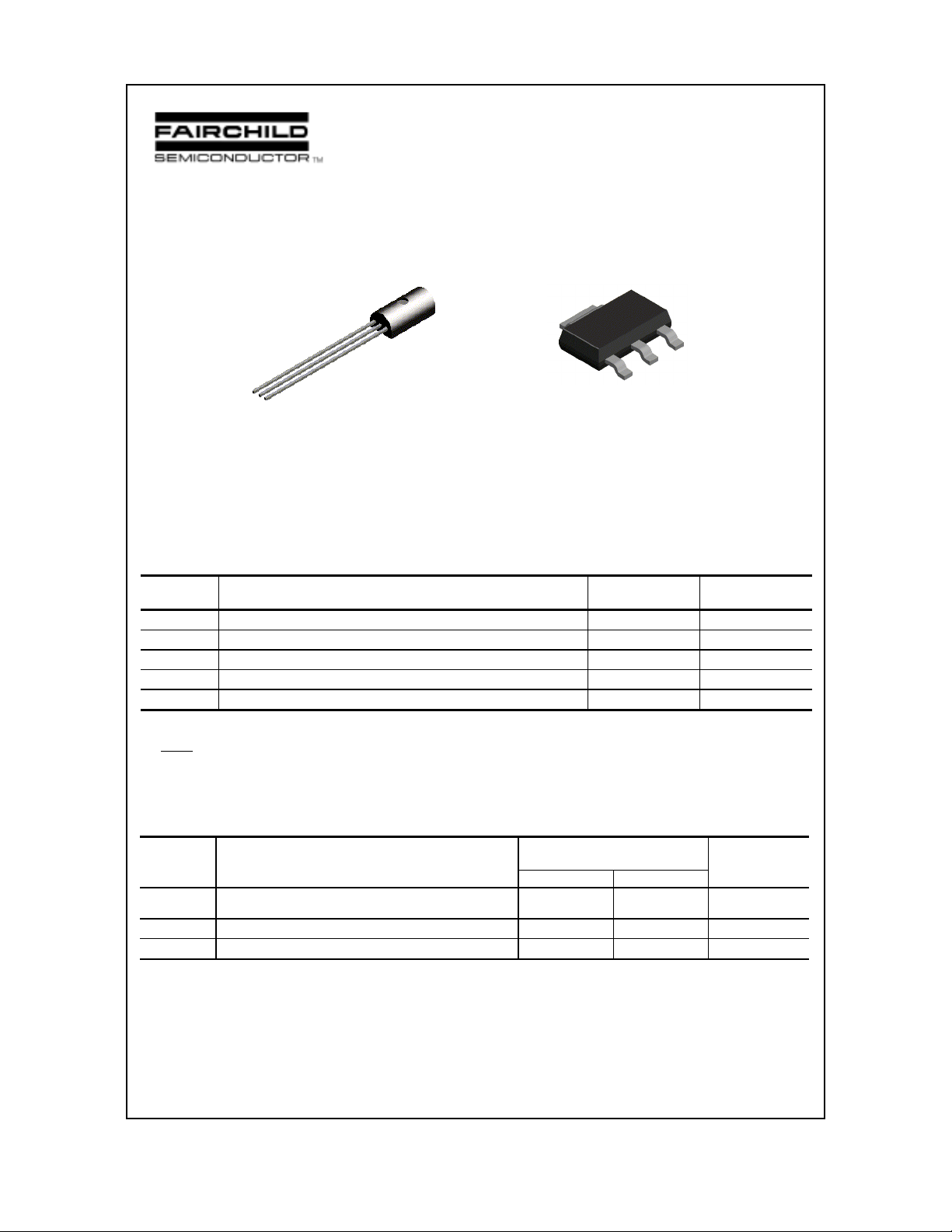
TN6714A / NZT6714
TN6714A
C
B
E
TO-226
NZT6714
C
E
C
B
SOT-223
NPN General Purpose Amplifier
This device is designed for general purpose medium power
amplifiers and switches requiring collector currents to 1.5 A.
Sourced from Process 37.
Absolute Maximum Ratings* TA = 25°C unless otherwise noted
Symbol Parameter Value Units
V
CEO
V
CBO
V
EBO
I
C
TJ, T
stg
*These ratings are limiting values above which the serviceability of any semiconductor device may be impaired.
NOTES:
1) These ratings are based on a maximum junction temperature of 150 degrees C.
2) These are steady state limits. The factory should be consulted on applications involving pulsed or low duty cycle operations.
Collector-Emitter Voltage 30 V
Collector-Base Voltage 40 V
Em i t ter - Bas e V olt ag e 5. 0 V
Collector Current - Continuous 2.0 A
Operating and Storage Junction Temperature Range -55 to +150
°C
Thermal Characteristics TA = 25°C unless otherwise noted
Symbol Characteristic Max Units
TN6714A *NZT6714
P
D
R
θ
JC
R
θ
JA
*Device mounted on FR-4 PCB 36 mm X 18 mm X 1.5 mm; mounting pad for the collector lead min. 6 cm
1997 Fairchild Semiconductor Corporation
Total De vice Dissip at i on
Derate above 25°C
Thermal Resistance, Junction to Case 50
Thermal Resistance, Junction to Ambient 125 125 °C/W
1.0
8.0
1.0
8.0
2
.
W
mW/°C
°C/W
NPN General Purpose Amplifier
(continued)
Electrical Characteristics TA= 25°C unless otherwise noted
Symbol Parameter Test Conditions Min Max Units
OFF CHARACTERISTICS
V
(BR)CEO
V
(BR)CBO
V
(BR)EBO
I
CBO
I
EBO
ON CHARACTERISTICS
h
FE
V
sat
CE(
V
BE(on)
SMALL SIGNAL CHARACTERISTICS
h
fe
C
cb
*Pulse Test: Pulse Width ≤ 300 µs, Duty Cycle ≤ 1.0%
Collector-Emitter Breakdown Voltage* IC = 10 mA, IB = 030V
C oll ec t or -Base Breakd ow n Volt age IC = 100 µA, IE = 0 40 V
Em i t ter - Bas e B r e akdown Vol tage
= 100 µA, IC = 0
I
E
Collector-Cutoff Current VCB = 40 V, IE = 0 0.1
Em i t ter - Cutoff C u r rent VEB = 5.0 V, IC = 0 0.1
DC Cu r re n t Ga in IC = 10 mA, VCE = 1.0 V
= 100 mA, VCE = 1.0 V
I
C
I
= 1.0 A, VCE = 1.0 V
Collector-Emitter Saturation Voltage IC = 1.0 A, IB = 100 mA 0.5 V
)
C
5.0 V
55
60
50 250
µ
A
µ
A
Base-Emitter On Voltage IC = 1.0 A, VCE = 1.0 V 1.2 V
Small-Signal Current Gain IC = 50 mA, VCE = 10 V,
2.5 25
f = 20 MHz
Collector-Base Capacitance VCB = 10 mA, IE = 0, f = 1.0 MHz 30 pF
TN6714A / NZT6714
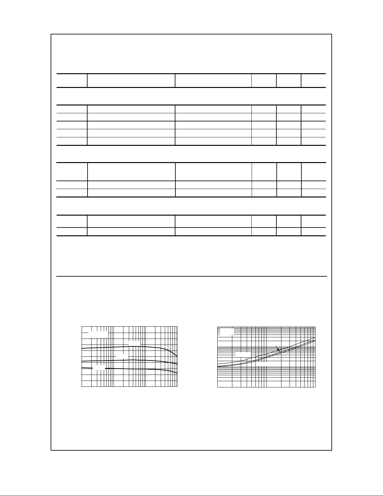
Typical Characteristics
Ty pical Pulsed Curr ent Ga in
vs Collector Current
500
V = 5V
400
300
200
100
FE
h - TYPICAL PULSED CURRENT GAIN
CE
125 °C
25 °C
- 40 ºC
0
0.001 0.01 0.1 1
C
I - COLLECTO R CURR ENT (A)
Collector-Emitter Saturation
Voltage vs Collector Current
1
ββ
= 10
0.1
125 ºC
0.01
0.01 0.1 1
CESAT
V - COLLECTOR-EMITTER VOLTAGE (V)
I - COLLEC TOR CU RREN T (A)
C
25 °C
- 40 ºC
 Loading...