

Fairchild Semiconductor TN3440A Datasheet
TN3440A
TN3440A
Discrete POWER & Signal
Technologies
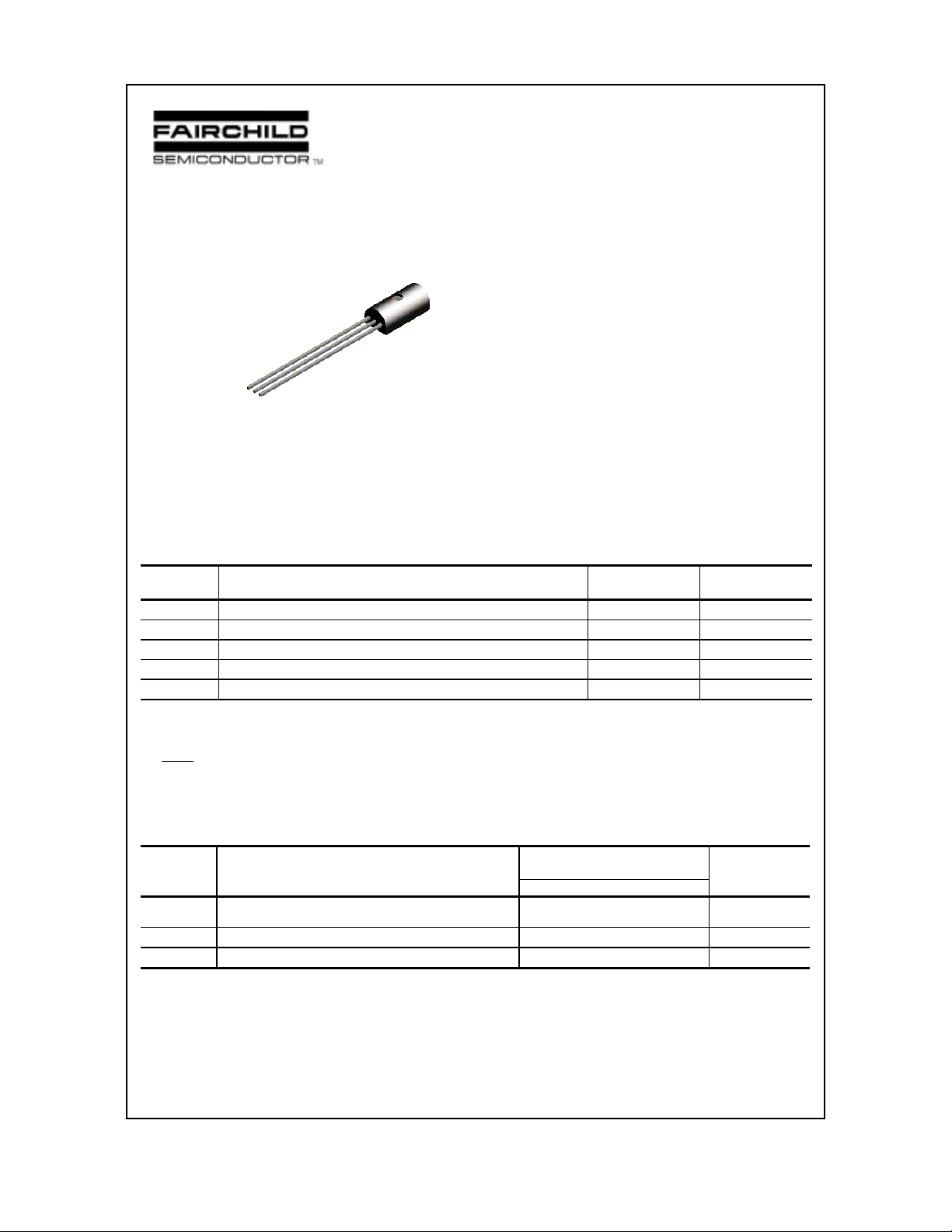
C
B
E
TO-226
NPN General Purpose Amplifier
This device is designed for use in horizontal driver, class A off-line
amplifier and off-line switching applications. Sourced from Process 36.
Absolute Maximum Ratings* TA = 25°C unless otherwise noted
Symbol Parameter Value Units
V
CEO
V
CBO
V
EBO
I
C
TJ, T
stg
*These ratings are limiting values above which the serviceability of any semiconductor device may be impaired.
NOTES:
1) These ratings are based on a maximum junction temperature of 150 degrees C.
2) These are steady state limits. The factory should be consulted on applications involving pulsed or low duty cycle operations.
Thermal Characteristics TA = 25°C unless otherwise noted
Collector-Emitter Voltage 250 V
Collector-Base Voltage 300 V
Em i t ter - Bas e V olt ag e 7. 0 V
Collector Current - Continuous 100 mA
Operating and Storage Junction Temperature Range -55 to +150
°C
Symbol Characteristic Max Units
TN3440A
P
D
R
θ
JC
R
θ
JA
1997 Fairchild Semiconductor Corporation
Total De vice Dissip at i on
Derate above 25°C
Thermal Resistance, Junction to Case 125 °C/W
Thermal Resistance, Junction to Ambient 50
1.0
8.0
W
mW/°C
°C/W
NPN General Purpose Amplifier
(continued)
Electrical Characteristics TA = 25°C unless otherwise noted
Symbol Parameter Test Conditions Min Max Units
OFF CHARACTERISTICS
V
sus
CEO(
V
(BR)CBO
I
CEO
I
CEX
I
CBO
I
EBO
ON CHARACTERISTICS
h
FE
V
sat
CE(
V
sat
BE(
SMALL SIGNAL CHARACTERISTICS
f
T
C
obo
C
ibo
h
fe
*Pulse Test: Pulse Width ≤ 300 µs, Duty Cycle ≤ 1.0%
Collector-Emitter Sustaining Voltage* IC = 50 mA, IB = 0 250 V
)
C ollector-B ase Breakdo w n Volt age
Co llector-C utoff Cur ren t VCE = 200 V, I
Co llector-C utoff Cur ren t VCE = 300 V, V
Co llector-C utoff Cur ren t VCB = 250 V, I
Emitter-Cutoff Current VEB = 5.0 V, I
= 100 µA, IE = 0
I
C
= 0 50
B
= 1.5 V 500
BE
= 0 20
E
= 0 20
C
DC Cu r re n t Ga in IC = 2.0 m A, VCE = 10 V
I
= 20 mA, VCE = 10 V
Collector-Emitter Saturation Voltage IC = 50 mA, IB = 4.0 mA 0.5 V
)
Base-Emitter Saturation Voltage IC = 50 mA, IB = 4.0 mA 1.3 V
)
C
Current Gain - Bandwidth Product IC = 10 mA, VCE = 10 V,
300 V
30
40 160
15 MHz
f = 5. 0 MHz
Output Capacitance VCB = 10 V, IE = 0, f = 1.0 MHz 10 pF
Input Capacitance VBE = 5.0 V, IC = 0, f = 1.0 MHz 95 pF
Small-Signal Current Gain IC = 5.0 m A, VCE = 10 V,
25
f = 1. 0 kHz
µ
A
µ
A
µ
A
µ
A
TN3440A
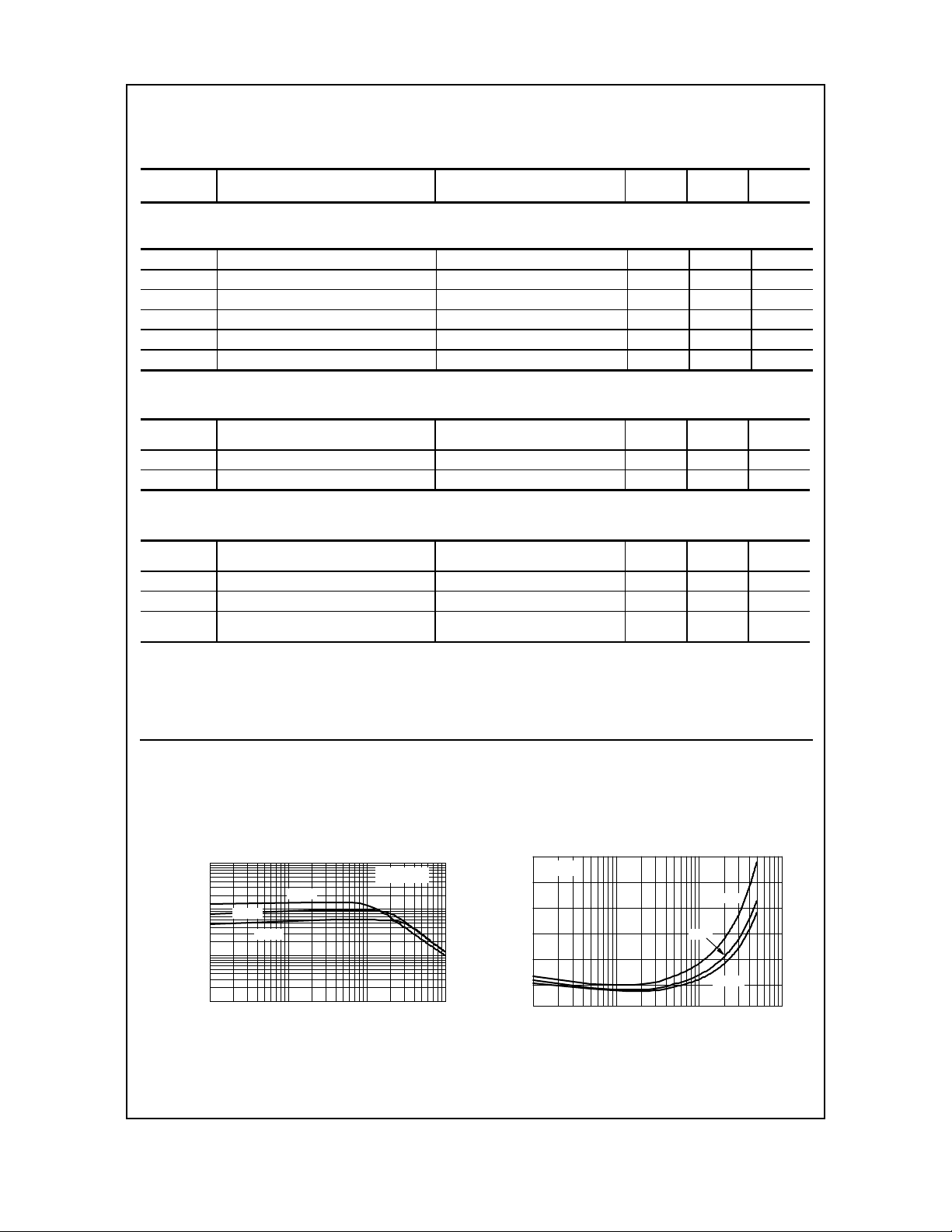
DC Typical Characteristics
Typical Pulsed Current Gain
vs Collector Current
1000
125 °C
100
FE
h - TYPICAL PULSED CURRENT GAIN
25 °C
- 40 ºC
10
1
0.001 0.01 0.1 1
I - COLLECTOR CURRENT (A)
C
V = 5V
CE
Collector-Emitter Saturation
Voltage vs Collector Current
0.3
ββ
= 10
0.2
0.1
1 10 100 1000
CESAT
V - COLLECTOR-EMITTER VOLTAGE (V)
I - COLLEC TOR CUR RE NT (mA)
C
125 °C
25 °C
- 40 ºC
 Loading...