

Fairchild Semiconductor TN2219A Datasheet
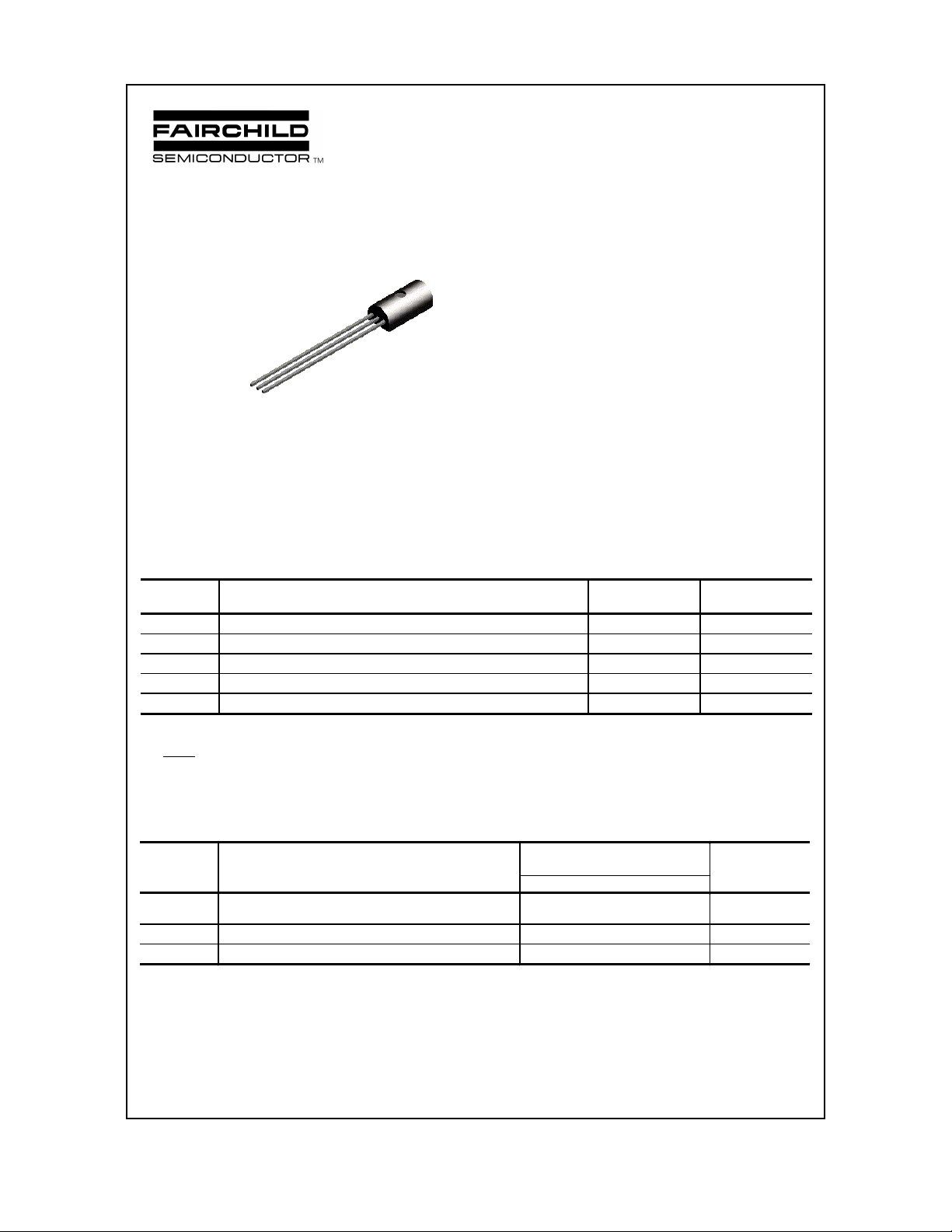
TN2219A
g
TN2219A
C
B
E
TO-226
NPN General Purpose Amplifier
This device is for use as a medium power amplifier and switch requiring
collector currents up to 500 mA. Sourced from Process 19. See
PN2222A for characteristics.
Absolute Maximum Ratings* TA = 25°C unless otherwise noted
Symbol Parameter Value Units
V
CEO
V
CBO
V
EBO
I
C
TJ, T
st
*These ratings are limiting values above which the serviceability of any semiconductor device may be impaired.
NOTES:
1) These ratings are based on a maximum junction temperature of 150 degrees C.
2) These are steady state limits. The factory should be consulted on applications involving pulsed or low duty cycle operations.
Thermal Characteristics TA = 25°C unless otherwise noted
Collector-Emit t er Vol tage 40 V
Collector-Base Voltage 75 V
Emitter-Base Voltage 6.0 V
Collector Current - Continuous 1.0 A
Operating and Stora ge Junction Temperature Range -55 to +150
C
°
Symbol Characteristic Max Units
TN2219A
P
D
R
θ
JC
R
θ
JA
1997 Fairchild Semiconductor Corporation
Total Device Dissipation
Derate above 25°C
1.0
8.0
Thermal Resistance, Junction to Case 125
Thermal Resistance, Junc tion to Ambient 50
W
mW/°C
°
C/W
°
C/W
TN2219A, Rev B
(BR)
(BR)
(BR)
µ
)
NPN General Purpose Amplifier
(continued)
Electrical Characteristics TA = 25°C unless otherwise noted
Symbol Parameter Test Conditions Min Max Units
OFF CHARACTERISTICS
V
CEO
V
CBO
V
EBO
I
CEX
I
CBO
I
EBO
I
BL
ON CHARACTERISTICS
h
FE
V
sat
CE(
V
sat
BE(
Collector-Emitter Breakdown Voltage* IC = 10 mA, IB = 0 40 V
Collector-Base Breakdown Voltage
Emitter-Base Breakdown Voltage
Collector Cu toff Current V
I
= 10 µA, IE = 0
C
I
= 10 µA, IC = 0
E
= 60 V, V
CE
Collector Cu toff Current VCB = 60 V, I
= 60 V, I
V
CB
Emitter Cutoff Current VEB = 3.0 V, I
Base Cutoff Curren t VCE = 60 V, V
DC Current Gain IC = 0.1 mA, VCE = 10 V
I
= 1.0 mA, VCE = 10 V
C
I
= 10 mA, VCE = 10 V
C
= 150 mA, VCE = 10 V
I
C
I
= 150 mA, VCE = 1.0 V
C
I
= 500 mA, VCE = 10 V
Collector-Emitter Saturation Voltage* IC = 150 mA, IB = 15 mA
)
Base-Emitter Saturation Voltage* IC = 150 mA, IB = 1.0 mA
)
C
I
= 500 mA, IB = 50 mA
C
= 500 mA, IB = 5.0 mA
I
C
= 3.0 V 10 nA
EB(OFF)
= 0
E
= 0, TA = 150°C
E
= 0 10 nA
C
= 3.0 20 nA
EB(OFF)
75 V
6.0 V
35
50
75
100
50
40
0.6 1.2
10
10
300
0.3
1.0
2.0
nA
A
V
V
V
V
TN2219A
SMALL SIGNAL CHARACTERISTICS
C
obo
C
ibo
h
fe
rb’C
C
NF Noise Figure
Re(h
ie
Output Capacitance VCB = 10 V, IE = 0, f = 100 kHz 8.0 pF
Input Capacitance VEB = 0.5 V, IC = 0, f = 100 kHz 25 pF
Small-Signal Current Gain IC = 1.0 mA, V
Collector Base Time Constant IE = 20 mA, VCB = 20 V, f = 31.8 MHz 150 pS
Real Part of Common-Emitter
)
High Frequency Input Impeda nce
SWITCHING CHARACTERISTICS
t
d
t
r
t
s
t
f
Delay Tim e VCC = 30 V, V
Rise Time IC = 150 mA, IB1 = 15 mA 25 ns
Storage Time VCC = 30 V, IC = 150 mA, 225 ns
Fall Time IB1 = IB2 = 15 mA 60 ns
*Pulse Test: Pulse Width ≤ 300 µs, Duty Cycle ≤ 2.0%
= 10 V, f = 1.0 kHz
I
= 10 mA, V
C
= 100 µA, V
I
C
R
= 1.0 kΩ, f = 1.0 kHz, BW = 1.0 Hz
S
CE
= 10 V, f = 1.0 kHz
CE
= 10 V,
CE
50
75
300
375
4.0 dB
IC = 20 mA, VCE = 20 V, f = 300 MHz 60
= 0.5 V, 10 ns
BE(OFF
Ω
 Loading...