

Fairchild Semiconductor TMC3003X30 Datasheet
www.fairchildsemi.com
REV. 1.0.3 3/5/01
Features
• 10-bit resolution
• 80, 50, and 30 megapixels per second
• Sync and blank controls
• Sync on green D/A output
• 1.0V p-p video into 37.5 Ω or 75 Ω load
• Enhancement of ADV7122
– Internal bandgap voltage reference
– Double-buffered data for low distortion
• TTL-compatible inputs
• Low glitch energy
• Single +5 Volt power supply
Applications
• Video signal conversion
– RGB
– YC
B
C
R
– Composite, Y, C
• Multimedia systems
• Image processing
• True-color graphics systems (1 billion colors)
• Broadcast television equipment
• High-Definition Television (HDTV) equipment
• Direct digital synthesis
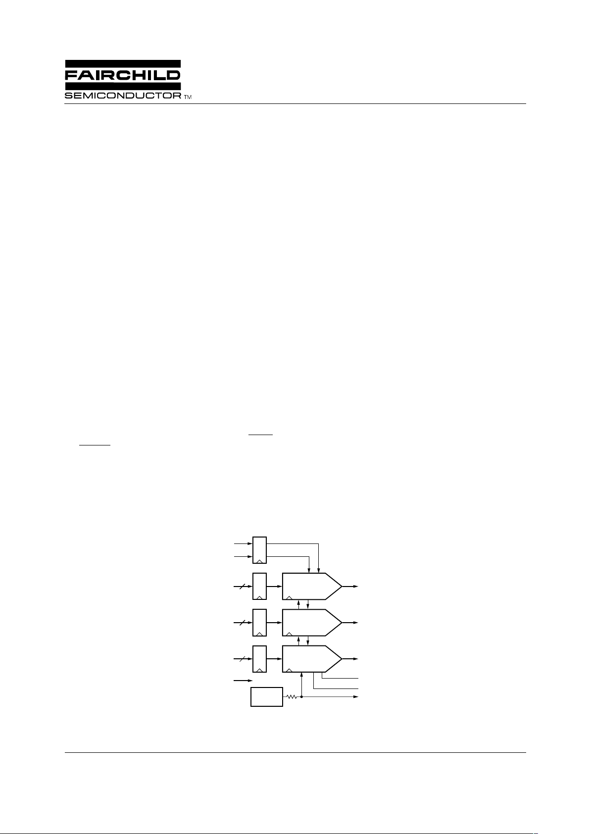
Block Diagram
10 bit
D/A Converter
10 bit
D/A Converter
10 bit
D/A Converter
10
G
9-0
BLANK
SYNC
CLK
IO
G
IO
B
IO
R
V
REF
R
REF
COMP
65-3003-01
+1.235V
Ref
10
B
9-0
10
R
9-0
Description
The TMC3003 is a high-speed triple 10-bit D/A converter
especially suited for video and graphics applications.
It offers 10-bit resolution, TTL-compatible inputs, low
power consumption, and requires only a single +5 Volt
power supply. It has single-ended current outputs, SYNC
and BLANK control inputs, and a separate current source for
adding sync pulses to the Green D/A converter output. It is
ideal for generating analog RGB from digital RGB and
driving computer display and video monitors. Three speed
grades are available: 30, 50, and 80 Msps.
The TMC3003 triple D/A converter is available in a 44-lead
plastic J-leaded PLCC and 48-Lead quad flatpack (LQFP).
It is fabricated on a sub-micron CMOS process with performance guaranteed from 0°C to 70°C.
TMC3003
Triple Video D/A Converter
10 bit, 80 Msps
TMC3003 PRODUCT SPECIFICATION
2
2
REV. 1.0.3 3/5/01
Functional Description
The TMC3003 is a low-cost triple 10-bit CMOS D/A
converter designed to directly drive computer CRT displays
and video transmission lines at pixel rates of up to 80 Msps.
It comprises three identical 10-bit D/A converters with
registered data inputs, common clock, and internal voltage
reference. An independent current source allows sync to be
added to the green D/A converter output.
Digital Inputs
All digital inputs are TTL-compatible. Data are registered on
the rising edge of the CLK signal. The analog output
changes t
DO
after the rising edge of CLK. There is one stage
of pipeline delay on the chip. The guaranteed clock rates of
the TMC3003 are 80, 50, and 30 MHz.
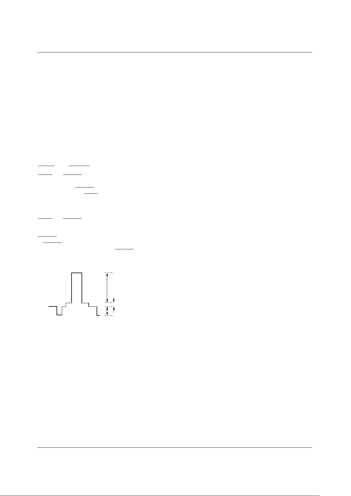
SYNC
and BLANK
SYNC and BLANK inputs control the output level
(Figure 1 and Table 1) of the D/A converters during CRT
retrace intervals. BLANK forces the D/A outputs to the
blanking level while SYNC turns off a separate current
source which is connected to the green D/A converter. This
connection adds a 40 IRE sync pulse to the D/A output and
brings that D/A output to 0.0 Volts during the sync tip.
SYNC and BLANK are registered on the rising edge of
CLK.
BLANK gates the D/A inputs and sets the pedestal voltage.
If BLANK = HIGH, the D/A inputs are added to a pedestal
which offsets the current output. If BLANK = LOW, data
inputs and the pedestal are disabled.
Figure 1. Nominal Output Levels
data: 660 mV max.
65-3003-02
pedestal: 54 mV
sync: 286 mV
D/A Outputs
Each D/A output is a current source. To obtain a voltage output a resistor must be connected to ground. Output voltage of
the D/A converters depends upon this resistor, the reference
voltage, and the value of the gain-setting resistor connected
between R
REF
and GND.
Normally, a source termination resistor of 75 Ohms is connected between the D/A current output pin and GND near
the D/A converter. A 75 Ohm coaxial cable may then be connected with another 75 Ohm termination resistor at the far
end of the cable. This “double termination” presents the D/A
converter with a net resistive load of 37.5 Ohms.
The TMC3003 may also be operated with a single 75 Ohm
terminating resistor. To lower the output voltage swing to the
desired range, the value of the resistor on R
REF
should be
increased.
Voltage Reference
The TMC3003 has an internal bandgap voltage reference
of +1.235 Volts. An external voltage reference may be
connected to the V
REF
pin, overriding the internal voltage
reference. All three D/A converters are driven from the same
reference.
A 0.1µF capacitor must be connected between the COMP
pin and V
DD
to stabilize internal bias circuitry and ensure
low-noise operation.
Power and Ground
The TMC3003 D/A converter requires a single +5.0 Volt
power supply. The analog (V
DD
) power supply voltage
should be decoupled to GND to reduce power supply
induced noise. 0.1µF decoupling capacitors should be placed
as close as possible to the power pins.
The high slew-rate of digital data makes capacitive coupling
to the outputs of any D/A converter a potential problem.
Since the digital signals contain high-frequency components
of the CLK signal, as well as the video output signal, the
resulting data feedthrough often looks like harmonic distortion or reduced signal-to-noise performance. All ground pins
should be connected to a common solid ground plane for
best performance.
PRODUCT SPECIFICATION TMC3003
REV. 1.0.3 3/5/01
3
Table 1. Output Voltage versus Input Code, SYNC
, and BLANK
V
REF
= 1.235 V, R
REF
= 590 Ω , R
L
= 37.5 Ω
Pin Assignments
RGB
9-0
(MSB...LSB)
Red and Blue D/As Green D/A
SYNC BLANK V
OUT
SYNC BLANK V
OUT
11 1111 1111 X 1 0.7140 1 1 1.0000
11 1111 1110 X 1 0.7134 1 1 0.9994
11 1111 1101 X 1 0.7127 1 1 0.9987
• ••••••
• ••••••
10 0000 0000 X 1 0.3843 1 1 0.6703
01 1111 1111 X 1 0.3837 1 1 0.6697
• ••••••
• ••••••
00 0000 0010 X 1 0.0553 1 1 0.3413
00 0000 0001 X 1 0.0546 1 1 0.3406
00 0000 0000 X 1 0.0540 1 1 0.3400
xx xxxx xxxx X 0 0.0000 1 0 0.2860
xx xxxx xxxx X 0 0.0000 0 0 0.0000
65-3003-03
G
1
G
2
G
3
G
4
G
5
G
6
G
7
G
8
G
9
BLANK
SYNC
R
REF
V
REF
COMP
IO
R
IO
G
V
DD
V
DD
IO
B
GND
GND
CLK
G0R9R8R7R6R5R4R3R2R1R
0
V
DD
B0B1B2B3B4B5B6B7B8B
9
7
8
9
10
11
12
13
14
15
16
17
39
38
37
36
35
34
33
32
31
30
29
1819202122232425262728
65432
1
4443424140
TMC3003
65-3003-05
G
1
G
2
G
3
G
4
G
5
G
6
G
7
G
8
G
9
BLANK
V
DD
R2R1NC
R
REF
V
REF
COMP
IO
G
IO
R
OV
DD
V
DD
IO
B
GND
GND
NC
G0R9R8R7R6R5R4R
3
NC
B
0B1B2B3B4B5B6B8B7
NC
1
2
3
4
5
6
7
8
9
10
SYNC
11
12
36
35
34
33
32
31
30
29
28
27
CLOCK
26
25
131415161718192021
22
B
9
23
24
484746454443424140
39
R
0
38
37
TMC3003
LQFPPLCC
TMC3003 PRODUCT SPECIFICATION
4
REV. 1.0.3 3/5/01
Pin Descriptions
Pin Name
Pin Number
Value DescriptionPLCC LQFP
Clock and Pixel I/O
CLK 29 26 TTL
Clock. The clock input is TTL-compatible and all pixel data
is registered on the rising edge of CLK. It is recommended
that CLK be driven by a dedicated TTL buffer to avoid
reflection induced jitter, overshoot, and undershoot.
R
9-0
5, 4, 3, 2, 1,
44, 43, 42,
41, 40
47, 46, 45,
44, 43, 42,
41, 40, 39,
38, 37
TTL
Red pixel data inputs. The Red digital input is TTL-
compatible and registered on the rising edge of CLK.
G
9-0
15, 14, 13,
12, 11, 10, 9,
8, 7, 6
48, 9, 8, 7, 6,
5, 4, 3, 2, 1
TTL
Green pixel data inputs. The Green digital input is TTL-
compatible and registered on the rising edge of CLK.
B
9-0
28, 27, 26,
25, 24, 23,
22, 21, 20,
19
23, 22, 21,
20, 19, 18,
17, 16, 15,
14
TTL
Blue pixel data inputs. The Blue digital input is TTL-
compatible and registered on the rising edge of CLK.
Controls
SYNC 17 11 TTL
Sync pulse Input. Bringing SYNC LOW, turns off a 40
IRE (7.62 mA) current source which forms a sync pulse on
the Green D/A converter output. SYNC is registered on the
rising edge of CLK along with pixel data and has the same
pipeline latency as BLANK and pixel data. SYNC does not
override any other data and should be used only during
the blanking interval.
Since this is a single-supply D/A and all signals are
positive-going, sync is added to the bottom of the Green
D/A range. So turning SYNC OFF means turning the
current source ON. When a sync pulse is desired, the
current source is turned OFF. If the system does not
require sync pulses from the Green D/A converter, SYNC
should be connected to GND.
BLANK 16 10 TTL
Blanking Input. When BLANK is LOW, pixel inputs are
ignored and the D/A converter outputs are driven to the
blanking level. BLANK is registered on the rising edge of
CLK and has the same pipeline latency as SYNC.
Video Outputs
IO
R
36 33 0.714 Vp-p Red D/A output. The current source outputs of the D/A
converters are capable of driving RS-343A/SMPTE-170M
compatible levels into doubly-terminated 75 Ohm lines.
IO
G
35 32 1 V p-p Green D/A output. The current source outputs of the D/A
converters are capable of driving RS-343A/SMPTE-170M
compatible levels into doubly-terminated 75 Ohm lines.
Sync pulses may be added to the Green D/A output.
IO
B
32 29 0.714 Vp-p Blue D/A output. The current source outputs of the D/A
converters are capable of driving RS-343A/SMPTE-170M
compatible levels into doubly-terminated 75 Ohm lines.
 Loading...