Fairchild Semiconductor TMC2330A Datasheet
www.fairchildsemi.com
TMC2330A
Coordinate Transformer
16 x 16 Bit, 40 MOPS
Features
• Rectangular-to-Polar or Polar-to-Rectangular conversion
at guaranteed 40 MOPS pipelined throughput rate
• Polar data: 16-bit magnitude, 32-bit input/16-bit output
phase
• 16-bit user selectable two’s complement or sign-andmagnitude rectangular data formats
• Input register clock enables and asynchronous output
enables simplify interfacing
• User-configurable phase accumulator for waveform
synthesis and amplitude, frequency, or phase modulation
• Magnitude output data overflow flag (in Polar-toRectangular mode)
• Low power consumption CMOS process
• Single +5V power supply
• Available in a 120-pin plastic pin grid array package
(PPGA), 120-pin ceramic pin grid array package (CPGA),
120-pin MQFP to PPGA (MPGA) package, and 120-pin
metric quad flatpack package (MQFP)
Applications
• Scan conversion (phased array to raster)
• Vector magnitude estimation
• Range and bearing derivation
• Spectral analysis
• Digital waveform synthesis, including quadrature
functions
• Digital modulation and demodulation
Description
The TMC2330A VLSI circuit converts bidirectionally
between Cartesian (real and imaginary) and Polar (magnitude
and phase) coordinates at up to 40 MOPS (Million Operations
Per Second).
In its Rectangular-to-Polar mode, the TMC2330A can extract
phase and magnitude information or backward “map” from a
rectangular raster display to a radial (e.g., range-and-azimuth)
data set.
The Polar-to-Rectangular mode executes direct digital waveform
synthesis and modulation. The TMC2330A greatly simplifies
real-time image-space conversion between the radially-generated
image scan data found in radar, sonar, and medical imaging
systems, and raster display formats.
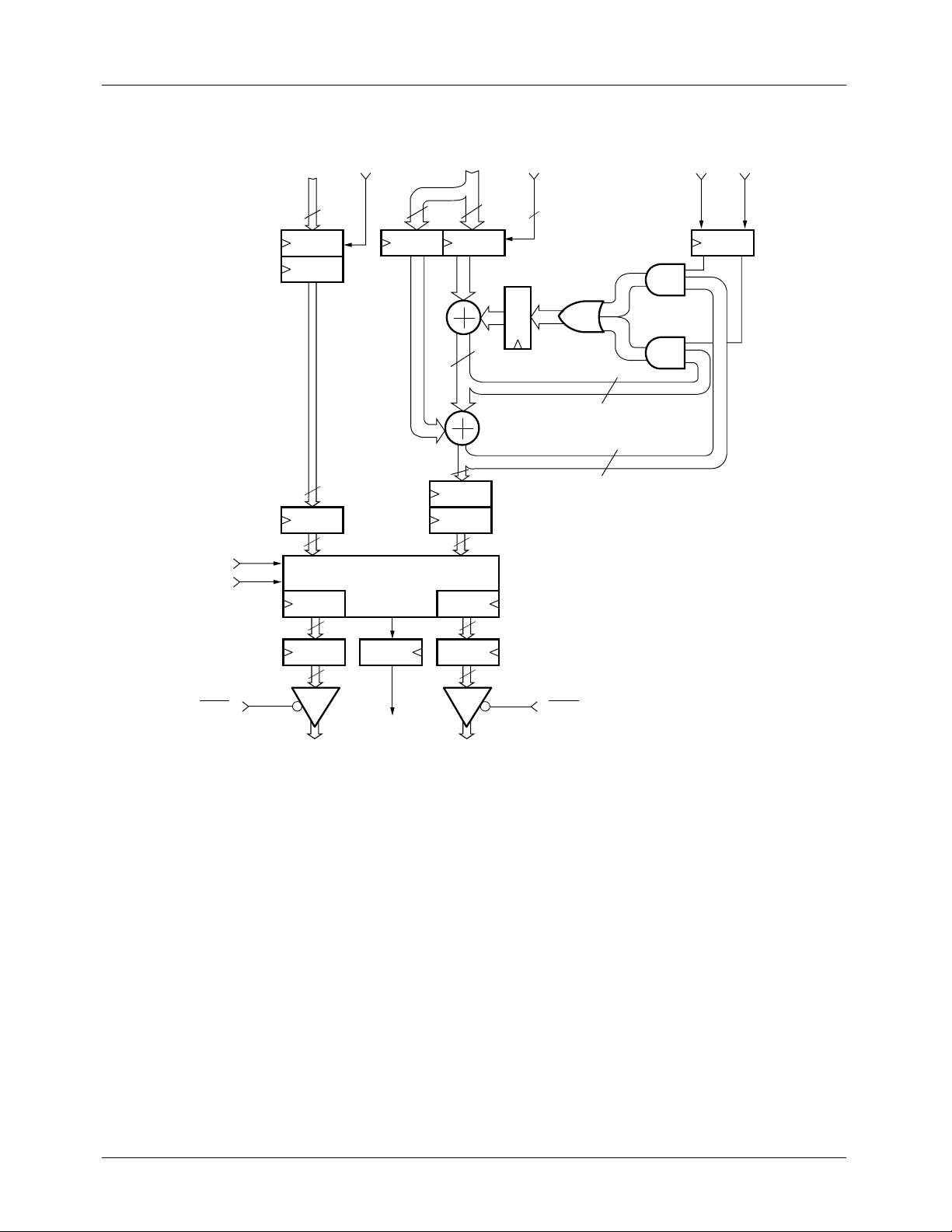
All input and output data ports are registered, and a new transformed data word pair is available at the output every clock
cycle. The user-configurable phase accumulator structure,
input clock enables, and asynchronous three-state output bus
enables simplify interfacing. All signals are TTL compatible.
Fabricated in a submicron CMOS process, the TMC2330A
operates at up to the 40 MHz maximum clock rate over the full
commercial (0 to 70°C) temperature and supply voltage ranges,
and is available in 120-pin plastic pin grid array, 120-pin
ceramic pin grid array, 120-pin metric quad flatpack to PPGA
package, and 120-pin metric quad flatpack packages.
Logic Symbol
CONFIGURATION
CONTROLS
DATA
INPUTS
ENXR
XRIN
ENYP
YPIN
ACC
TCXY
RTP
CLK
15-0
1-0
31-0
1-0
32
16
TMC2330A
OERX
16
RXOUT
15-0
DATA
OEPY
2
16
PYOUT
OVF
OUTPUTS
15-0
REV. 1.1.8 10/31/00
PRODUCT SPECIFICATION TMC2330A
Block Diagram
YPIN
XRIN
15-0
ENXR
31-0
ENYP
1-0
ACC
ACC
1
0
16
1
2
AM
16
3
16
TCXY
RPT
TRANSFORMATION PROCESS
4-21
16 16
22 22 22
16
32 32
16
2
3
4-21
2
CM
32
32
32
PM
FM
16
16
32
32
32
OERX
OVF
RXOUT
15-0
PYOUT
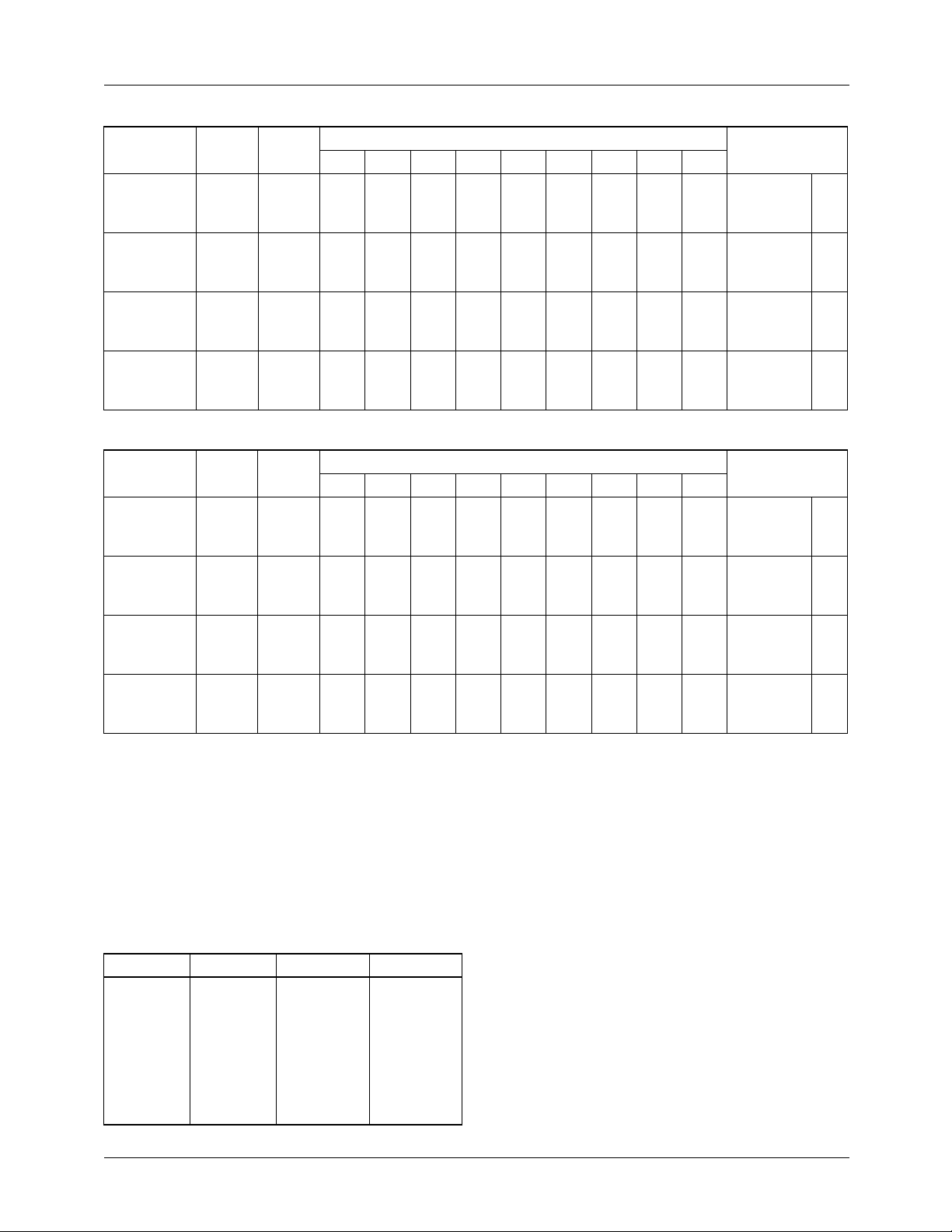
Functional Description
The TMC2330A converts between Rectangular (Cartesian)
and Polar (Phase and Magnitude) coordinate data word pairs.
The user selects the numeric format and transformation to be
performed (Rectangular-To-Polar or Polar-To-Rectangular),
and the operation is performed on the data presented to the
inputs on the next clock. The transformed result is then
available at the outputs 22 clock cycles later, with new output data available every 20ns with a 40 MHz clock. All input
and output data ports are registered, with input clock enables
and asynchronous high-impedance output enables to simplify connections to system buses.
OEPY
15-0
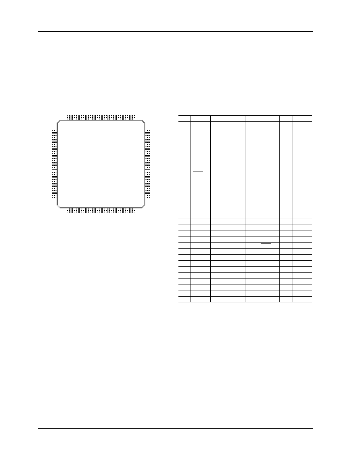
When executing a Rectangular-To-Polar conversion, the input
ports accept 16-bit Rectangular coordinate words, and the output ports generate 16-bit magnitude and 16-bit phase data. The
user selects either two’s complement or sign-and-magnitude
Cartesian data format. Polar magnitude data are always in
magnitude format only. Since the phase angle word is modulo
2 π , it may be regarded as either unsigned or two’s complement
format (Tables 1 and 2)
.
In Polar-To-Rectangular mode, the input ports accept 16-bit
Polar magnitude and 32-bit phase data, and the output ports
produce 16-bit Rectangular data words. Again, the user
selects between two’s complement or sign-and-magnitude
Cartesian data format.
2
REV. 1.1.8 10/31/00
(x π
(x π
(x π
TMC2330A PRODUCT SPECIFICATION
Table 1. Data Input/Output Formats—Integer Format
…
…
Bit #
-15
2
0
2
0
2
2
NS
–2
2
NS
–2
2
NS
–2
±2
15
-16
15
Format
14
2
2
15
2
2
14
14
-17
…
…
…
…
0
2
0
2
0
2
-31
2
)T/U
U
S
T
S
T
14
2
15
14
2
14
2
14
2
15
14
2
0
-1
2
0
2
0
2
0
2
0
2
0
2
-15
2
)T/U
S
T
U
S
T
Port RTP TCXY
XRIN
XRIN
XRIN
YPIN
YPIN
YPIN
RXOUT
RXOUT
RXOUT
PYOUT
PYOUT
PYOUT
0
1
1
0
1
1
0
0
1
0
0
1
X
0
1
X
0
1
0
1
X
0
1
X
31 30 29 … 16 15 14 … 0
0
-1
±2
NS
–2
2
2
15
2
-2
2
14
13
2
14
13
2
Table 2. Data Input/Output Formats—Fractional Format
…
…
…
Bit #
-15
2
-15
2
-15
2
2
NS
–2
-16
2
NS
–2
2
NS
–2
±2
Format
0
-1
…
2
-1
…
2
0
-1
2
…
-17
2
…
-15
2
-15
2
-15
2
-31
2
)T/U
U
S
T
S
T
-1
2
0
0
0
0
…
-1
…
2
-1
2
…
-1
…
2
-1
2
…
-1
2
…
-15
2
-15
2
-15
2
-15
2
-15
2
-15
2
)T/U
S
T
U
S
T
Port
XRIN
XRIN
XRIN
YPIN
YPIN
YPIN
RXOUT
RXOUT
RXOUT
PYOUT
PYOUT
PYOUT
RTP TCXY
0
1
1
0
1
1
0
0
1
0
0
1
X
0
1
X
0
1
0
1
X
0
1
X
31 30 29 … 16 15 14 … 0
0
-1
±2
NS
-2
2
2
0
2
-2
2
-1
-2
2
-1
-2
2
(x π
Notes:
15
1. -2
denotes two’s complement sign bit.
2. NS denotes negative sign, i.e., ‘1’ negates the number.
0
3. ±2
denotes two’s complement sign or highest magnitude bit – since phase angles are modulo 2 π and phase accumulator is
modulo 2
32
, this bit may be regarded as + π or - π .
4. All phase angles are in terms of π radians, hence notation “x π .”
5. If A
= 00, YPIN(15-0) are “don’t cares.”
CC
6. Formats:
T = Two’s Complement
S = Signed Magnitude
U = Unsigned
HEX U T S
FFFF
…
8001
8000
7FFF
…
0001
0000
REV. 1.1.8 10/31/00
65535
…
32769
32768
32767
…
1
0
–1
…
-32767
-32768
32767
…
1
0
-32767
…
-1
0
32767
…
1
0
3
PRODUCT SPECIFICATION TMC2330A
Static Control Inputs
The controls RTP and TCXY determine the transformation
mode and the assumed numeric format of the Rectangular
data. The user must exercise caution when changing either of
these controls, as the new transformed results will not be
seen at the outputs until the entire internal pipe (22 clocks)
has been flushed. Thus, these controls are considered static.
Pin Assignments
120-Pin MQFP
Pin Name Pin Name
31
VDD
Pin 1
1
PYOUT4
2
PYOUT3
3
GND
4
PYOUT2
5
PYOUT1
6
PYOUT0
7
VDD
8
OEPY
9
GND
10
RTP
11
CLK
12
GND
13
TCXY
14
ENPY
15
GND
16
ENPY1
17
ACC0
18
ACC1
19
VDD
20
YPIN0
21
YPIN1
22
YPIN2
23
YPIN3
24
YPIN4
25
YPIN5
26
YPIN6
27
GND
28
YPIN7
29
YPIN8
30
GND
32
YPIN9
33
YPIN10
34
VDD
35
YPIN11
36
YPIN12
37
YPIN13
38
YPIN14
39
YPIN15
40
YPIN16
41
YPIN17
42
VDD
43
YPIN18
44
YPIN19
45
YPIN20
46
GND
47
YPIN21
48
YPIN22
49
YPIN23
50
VDD
51
YPIN24
52
YPIN25
53
YPIN26
54
YPIN27
55
YPIN28
56
YPIN29
57
YPIN30
58
YPIN31
59
ENXR
60
XRIN0
Pin Name Pin Name
91
92
93
94
95
96
97
98
99
100
101
102
103
104
105
106
107
108
109
110
111
112
113
114
115
116
117
118
119
120
VDD
RXOUT9
RXOUT8
GND
RXOUT7
RXOUT6
RXOUT5
GND
RXOUT4
RXOUT3
RXOUT2
VDD
RXOUT1
RXOUT0
OVF
GND
PYOUT15
PYOUT14
PYOUT13
VDD
PYOUT12
PYOUT11
PYOUT10
GND
PYOUT9
PYOUT8
PYOUT7
GND
PYOUT6
PYOUT5
61
62
63
64
65
66
67
68
69
70
71
72
73
74
75
76
77
78
79
80
81
82
83
84
85
86
87
88
89
90
VDD
XRIN1
XRIN2
GND
XRIN3
XRIN4
XRIN5
GND
XRIN6
XRIN7
XRIN8
XRIN9
XRIN10
XRIN11
XRIN12
GND
XRIN13
XRIN14
XRIN15
VDD
OERX
GND
RXOUT15
VDD
RXOUT14
RXOUT13
RXOUT12
GND
RXOUT11
RXOUT10
4
REV. 1.1.8 10/31/00
TMC2330A PRODUCT SPECIFICATION
Pin Assignments (continued)
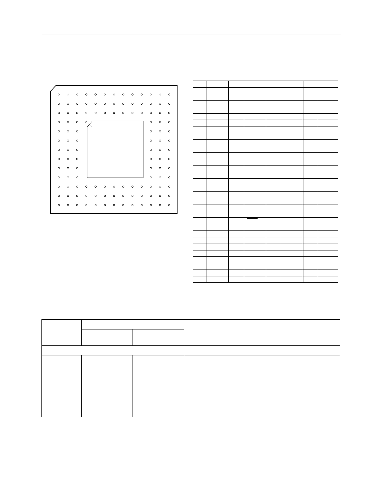
120-Pin PPGA, H5 Package and 120-Pin CPGA, G1 Package and 120-Pin Metric Quad Flatpack to
120-Pin Plastic Pin Array, H6 Package
12345678910111213
A
B
C
D
E
F
G
H
J
K
L
M
N
KEY
Top View
Cavity Up
Pin Name Pin Name
GND
A1
A2
A3
A4
A5
A6
A7
A8
A9
A10
A11
A12
A13
B1
B2
B3
B4
B5
B6
B7
B8
B9
B10
B11
B12
B13
C1
C2
C3
C4
PYOUT5
PYOUT7
PYOUT8
PYOUT10
PYOUT12
PYOUT14
PYOUT15
RXOUT0
RXOUT2
RXOUT4
RXOUT6
RXOUT8
RXOUT10
PYOUT3
PYOUT4
PYOUT6
PYOUT9
PYOUT11
PYOUT13
OVF
RXOUT1
RXOUT3
RXOUT5
RXOUT7
RXOUT9
RXOUT12
PYOUT1
PYOUT2
VDD
GND
C5
C6
C7
C8
C9
C10
C11
C12
C13
D1
D2
D3
D11
D12
D13
E1
E2
E3
E11
E12
E13
F1
F2
F3
F11
F12
F13
G1
G2
G3
VDD
GND
VDD
GND
GND
VDD
RXOUT11
RXOUT13
OEPY
PYOUT0
GND
GND
RXOUT14
RXOUT15
RTP
GND
VDD
VDD
GND
OERX
TCKY
GND
CLK
VDD
RXIN15
RXIN14
ENPY1
ENPY0
GND
Pin Name Pin Name
L10
L11
L12
L13
M1
M2
M3
M4
M5
M6
M7
M8
M9
M10
M11
M12
M13
N1
N2
N3
N4
N5
N6
N7
N8
N9
N10
N11
N12
N13
YPIN31
VDD
XRIN3
XRIN4
YPIN6
YPIN9
YPIN11
YPIN13
YPIN16
YPIN18
YPIN20
YPIN23
YPIN25
YPIN28
ENXR
XRIN1
XRIN2
YPIN8
YPIN10
YPIN12
YPIN15
YPIN17
YPIN19
YPIN21
YPIN22
YPIN24
YPIN26
YPIN29
YPIN30
XRIN0
G11
G12
G13
H1
H2
H3
H11
H12
H13
J1
J2
J3
J11
J12
J13
K1
K2
K3
K11
K12
K13
L1
L2
L3
L4
L5
L6
L7
L8
L9
GND
XRIN12
RXIN13
ACCO
ACC1
VDD
XRIN9
XRIN10
XRIN11
YPIN0
YPIN1
YPIN3
GND
XRIN7
XRIN8
YPIN2
YPIN4
GND
GND
XRIN5
XRIN6
YPIN5
YPIN7
GND
VDD
YPIN14
VDD
GND
VDD
YPIN27
Pin Descriptions
Pin Number
Pin Name
MQFP
CPGA/PPGA/
MPGA
Power, Ground and Clock
V
DD
1, 8, 20, 34, 42,
50, 61, 80, 84, 91,
102, 110
GND 4, 10, 13, 16, 28,
31, 46, 64, 68, 76,
82, 88, 94, 98,
106, 114, 118
C3, E3, H3, L4, L6,
L8, L11, F11, E11,
C11, C8, C6
D3, E2, F2, G3,
K3, L3, L7, K11,
J11, G11, E12,
D11, C10, C9, C7,
C5, C4
REV. 1.1.8 10/31/00 5
Description
The TMC2330A operates from a single +5V supply. All
power and ground pins must be connected.
Ground

PRODUCT SPECIFICATION TMC2330A
Pin Descriptions (continued)
Pin Number
Pin Name
MQFP
CPGA/PPGA/
MPGA
CLK 12 F3 The TMC2330A operates from a single clock. All enabled
Inputs/Outputs
XRIN
15-0
79, 78, 77, 75, 74,
73, 72, 71, 70, 69,
67, 66, 65, 63, 62,
60
F12, F13, G13,
G12, H13, H12,
H11, J13, J12,
K13, K12, L13,
L12, M13, M12,
N13
YPIN
31-0
58, 57, 56, 55, 54,
53, 52, 51, 49, 48,
47, 45, 44, 43, 41,
40, 39, 38, 37, 36,
35, 33, 32, 30, 29,
27, 26, 25, 24, 23,
22, 21
L10, N12, N11,
M10, L9, N10, M9,
N9, M8, N8, N7,
M7, N6, M6, N5,
M5, N4, L5, M4,
N3, M3, N2, M2,
N1, L2, M1, L1,
K2, J3, K1, J2, J1
RXOUT
83, 85, 86, 87, 89,
15-0
90, 92, 93, 95, 96,
97, 99, 100, 101,
103, 104
D13, D12, C13,
B13, C12, A13,
B12, A12, B11,
A11, B10, A10,
B9, A9, B8, A8
PYOUT
15-0
107, 108, 109,
111, 112, 113,
115, 116, 117,
119, 120, 2, 3, 5,
A7, A6, B6, A5,
B5, A4, B4, A3,
A2, B3, A1, B2,
B1, C2, C1, D2
6, 7
Controls
ENXR 59 M11 The value presented to the input port XRIN is latched into
ENYP
1,0
17, 15 G1, G2 The value presented to the YPIN input port is latched into
Description
registers are strobed on the rising edge of CLK, which is
the reference for all timing specifications.
XRIN
is the registered Cartesian X-coordinate or
15-0
Polar Magnitude (Radius) 16-bit input data port. XRIN15 is
the MSB.
YPIN
is the registered Cartesian Y-coordinate or Polar
31-0
Phase angle 32-bit input data port. The input phase
accumulators are fed through this port in conjunction with
the input enable select ENYP
. When RTP is HIGH
1,0
(Rectangular-To-Polar), the input accumulators are
normally not used. The 16 MSBs of YPIN are the input
port, and the lower 16 bits become “don’t cares” if ACC = 00.
YPIN31 is the MSB.
RXOUT
is the registered Polar Magnitude (Radius) or
15-0
X-coordinate 16-bit output data port. This output is forced
into the high-impedance state when OERX=HIGH.
RXOUT15 is the MSB.
PYOUT
is the registered Polar Phase angle or
15-0
Cartesian Y-coordinate 16-bit output data port. This output
is forced to the high-impedance state when OEPY=HIGH.
PYOUT15 is the MSB.
the input registers on the current clock when ENXR is
HIGH. When ENXR is LOW, the value stored in the
register remains unchanged.
the phase accumulator input registers on the current
clock, as determined by the control inputs ENYP
shown below:
1,0
, as
Register Operation
ENYP
MC
1,0
00 hold hold
01 load hold
10 hold load
11 clear load
where C is the Carrier register and M is the Modulation
register, and 0=LOW, 1=HIGH. See the Functional Block
Diagram.
6 REV. 1.1.8 10/31/00
 Loading...