

Fairchild Semiconductor TMC2249AX2 Datasheet
www.fairchildsemi.com
REV. 1.0.2 7/6/00
Features
• 60 MHz input and computation rate
• Two 12-bit multipliers
• Separate data and coefficient inputs
• Independent, user-selectable pipeline delays of 1 to 16
clocks on all input ports
• Separate 16-bit input port allows cascading or addition of
a constant
• User-selectable rounded output
• Internal 1/2 LSB rounding of products
• Fully registered, pipelined architecture
• Available in 120-Pin CPGA, PPGA, MPGA or MQFP
Applications
• Video switching
• Image mixing
• Digital signal modulation
• Complex frequency synthesis
• Digital filtering
• Complex arithmetic functions
Description
The TMC2249A is a high-speed digital arithmetic circuit
consisting of two 12-bit multipliers, an adder and a cascadeable accumulator. All four multiplier inputs are simultaneously accessible to the user, and each includes a userprogrammable pipeline delay of up to 16 clocks in length.
The 24-bit adder/subtractor is followed by an accumulator
and 16-bit input port which allows the user to cascade multiple TMC2249As. A new 16-bit accumulated output is available every clock, up to the maximum rate of 60 MHz. All
inputs and outputs are registered except the three-state output enable, and all are TTL compatible.
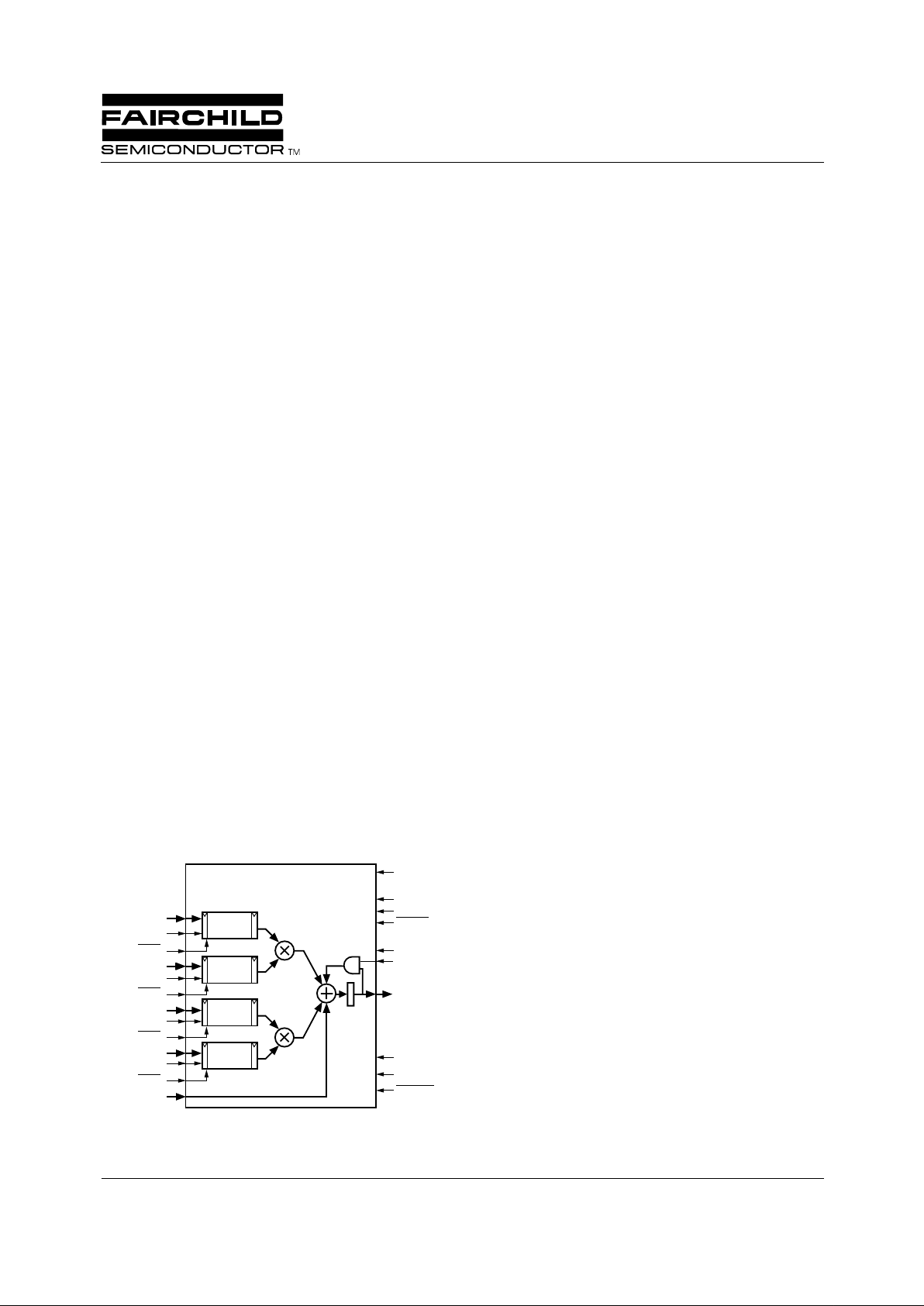
Logic Symbol
TMC2249A
Digital Mixer
CLK
NEG1
NEG2
SWAP
OE
ACC
RND
FT
CASEN
S
15-0
Delay
1-16
Delay
1-16
Delay
1-16
Delay
1-16
B
11-0
ADEL
3-0
A
11-0
BDEL
3-0
ENA
ENB
C
11-0
CDEL
3-0
ENC
D
11-0
CAB
15-0
DDEL
3-0
END
The TMC2249A utilizes a pipelined, bus-oriented structure
offering significant flexibility. Input register clock enables
and programmable input data pipeline delays on each port
offer an adaptable input structure for high-speed digital
systems. Following the multipliers, the user may perform
addition or subtraction of either product, arithmetic rounding
to 16 bits, and accumulation and summation of products with a
cascading input. The output port allows access to all 24 bits of
the internal accumulator by switching between overlapping
least and most-significant 16-bit words, and a three-state output enable simplifies connection to an external system bus.
The TMC2249A has numerous applications in digital processing algorithms, from executing simple image mixing and
switching, to performing complex arithmetic functions and
complex waveform synthesis. FIR filters, digital quadrature
mixers and modulators, and vector arithmetic functions may
also be implemented with this device.
Fabricated in a submicron CMOS process, the TMC2249A
operates at guaranteed clock rates of up to 60 MHz over the
full temperature and supply voltage ranges. It is pin- and
function-compatible with Fairchild’s TMC2249, while providing higher speed operation and lower power dissipation. It
is available in a 120 pin Ceramic Pin Grid Array (CPGA),
120 pin Plastic Pin Grid Array (PPGA), 120 lead MQFP to
PPGA package (MPGA), and a 120 lead Metric Quad FlatPack (MQFP).
TMC2249A
Digital Mixer
12 x 12 Bit, 60 MHz
PRODUCT SPECIFICATION TMC2249A
2
REV. 1.0.2 7/6/00
Block Diagram
ADEL
3-0
A
11-0
1-16
ENA BDEL
3-0
NEG1
NEG2
RND
FT
16
16
24
16
M
16
L
ACC
I0
01 01
2's Comp 2's Comp
CASEN
ACC
SWAP
OE
CAS
15-0
S
15-0
B
11-0
1-16
ENB
DDEL
3-0
D
11-0
1-16
ENDCDEL
3-0
C
11-0
1-16
ENC
124
12
E
E
E
1
2
16
12
12
01 F
12
12 x (16:1) MUX
12
12
12
ADEL
3-0
A
11-0
ENA

TMC2249A PRODUCT SPECIFICATION
REV. 1.0.2 7/6/00
3
Functional Description
The TMC2249A performs the summation of products
described by the formula:
S(N+5) =A(N-ADEL) × B(N-BDEL) × (-1
NEG1(N)
) +
C(N-CDEL) × D(N-DDEL) × (-1
NEG2(N)
) +
CAS(N+3 × FT)
where ADEL through DDEL range from 1 to 16 pipe delays.
All inputs and controls utilize pipeline delay registers to
maintain synchronicity with the data input during that clock,
except when the Cascade data input is routed directly to the
accumulator by use of the Feedthrough control. One-half
LSB rounding to 16 bits may be performed on the sum of
products while summing with the cascade input data.
The user may access either the upper or lower 16 bits of the
24-bit accumulator by swapping overlapping registers. The
output bus has an asynchronous high-impedance enable, to
simplify interfacing to complex systems.
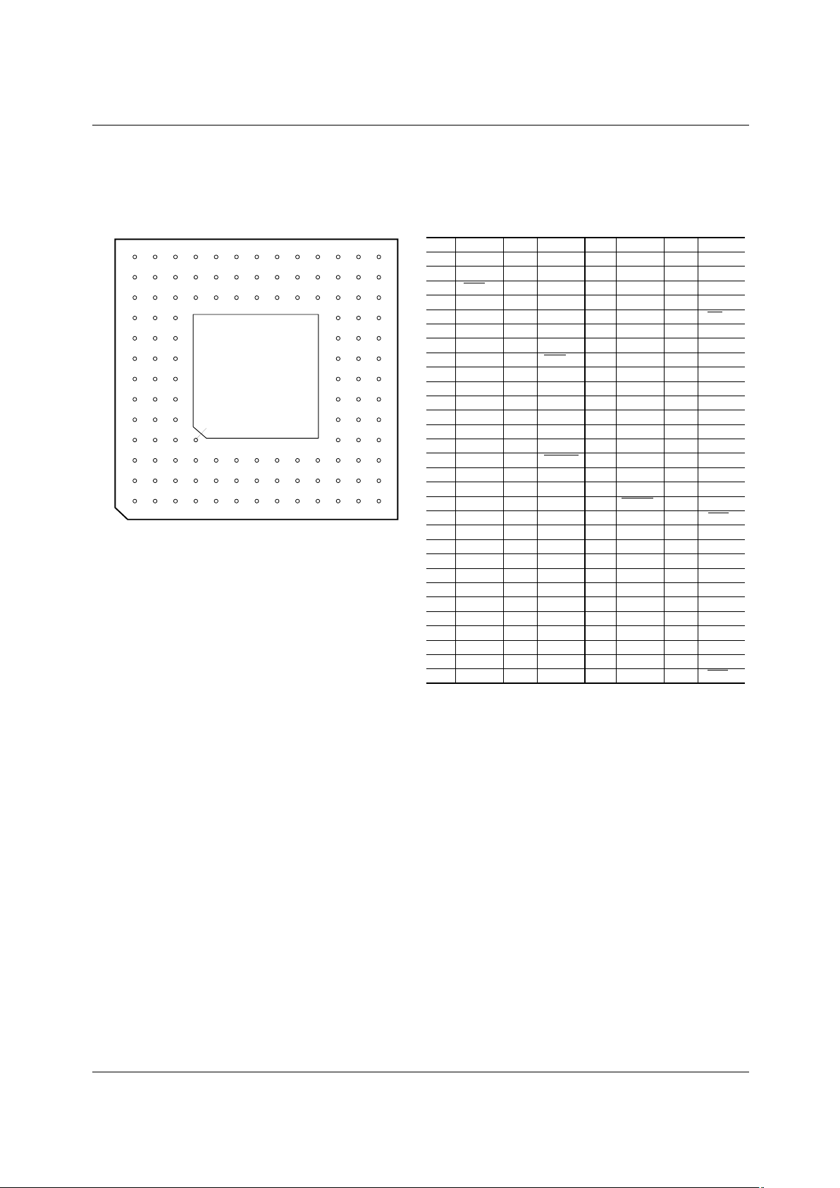
Pin Assignments
120 Pin Metric Quad Flat Pack, KE Package
CLK
ACC
NEG1
NEG2
RND
S
15
S
14
GND
S
13
S
12
S
11
V
DD
S
10
S
9
S
8
GND
S
7
S
8
S
5
V
DD
S
4
S
3
S
2
GND
S
1
S
0
OE
SWAP
BDEL
0
BDEL
1
1
30
120 91
31 60
1
2
3
4
5
6
7
8
9
10
11
12
13
14
15
16
17
18
19
20
21
22
23
24
25
26
27
28
29
30
90
61
BDEL
2
BDEL
3
ENB
B
0
B
1
B
2
B
3
B
4
B
5
B
6
B
7
GND
B
8
B
9
B
10
V
DD
B
11
A
11
A
10
A
9
A
8
A
7
A
6
A
5
A
4
A
3
A
2
A
1
A
0
ENA
31
32
33
34
35
36
37
38
39
40
41
42
43
44
45
46
47
48
49
50
51
52
53
54
55
56
57
58
59
60
Pin Name Pin Name
ADEL
3
ADEL
2
ADEL
1
ADEL
0
NC
CAS
15
CAS
14
CAS
13
CAS
12
CAS
11
CAS
10
GND
CAS
9
CAS
8
CAS
7
CAS
6
CAS
5
CAS
4
CAS
3
CAS
2
CAS
1
CAS
0
CASEN
FT
CDEL
0
CDEL
1
CDEL
2
CDEL
3
ENC
C
0
61
62
63
64
65
66
67
68
69
70
71
72
73
74
75
76
77
78
79
80
81
82
83
84
85
86
87
88
89
90
C
1
C
2
C
3
C
4
C
5
C
6
C
7
C
8
C
9
C
10
C
11
V
DD
D
11
D
10
D
9
GND
D
8
D
7
D
6
D
5
D
4
D
3
D
2
D
1
D
0
END
DDEL
3
DDEL
2
DDEL
1
DDEL
0
91
92
93
94
95
96
97
98
99
100
101
102
103
104
105
106
107
108
109
110
111
112
113
114
115
116
117
118
119
120
Pin Name Pin Name
PRODUCT SPECIFICATION TMC2249A
4
REV. 1.0.2 7/6/00
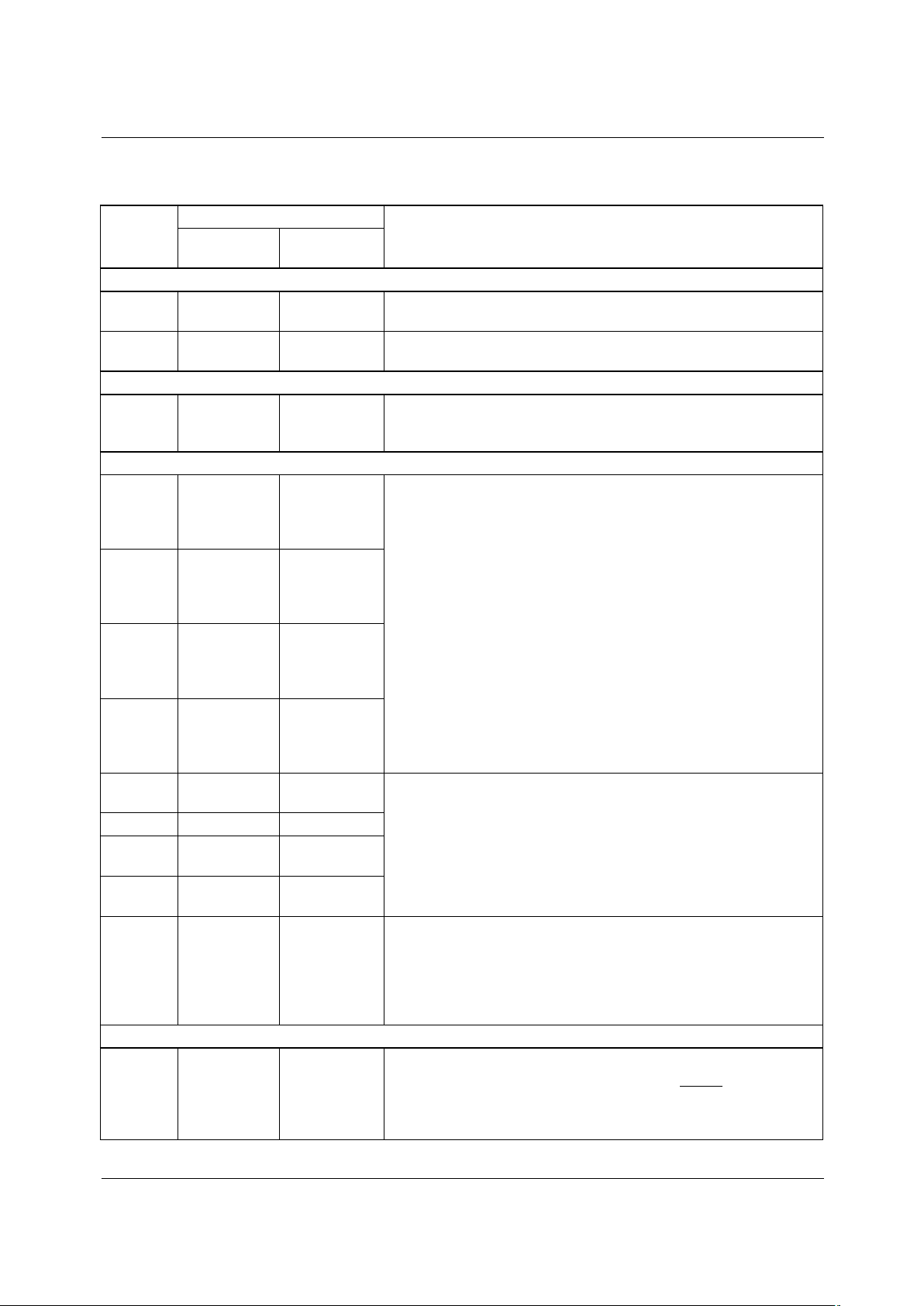
Pin Assignments
120 Pin Plastic Pin Grid Array, H5 Package, 120 Pin Ceramic Pin Grid Array, G1 Package, and
120 Pin Metric Quad FlatPack to 120 Pin Plastic Pin Array, H6 Package
BADEFGHJKLMNC
1
2
3
4
5
6
7
8
9
10
11
12
13
Top View
Cavity Up
KEY
DDEL
0
DDEL
3
END
D
2
D
4
D
7
D
8
D
10
C
11
C
9
C
6
C
3
C
0
NEG1
ACC
DDEL
1
D
0
D
3
D
6
D
9
D
11
C
10
C
7
C
5
C
2
CDEL
2
S
15
RND
CLK
DDEL
2
A1
A2
A3
A4
A5
A6
A7
A8
A9
A10
A11
A12
A13
B1
B2
B3
B4
B5
B6
B7
B8
B9
B10
B11
B12
B13
C1
C2
C3
C4
D
1
D
5
GND
V
DD
C
8
C
4
C
1
ENC
CDEL
1
S
13
S
14
GND
CDEL
3
CDEL
0
CASEN
S
11
S
12
GND
FT
CAS
0
CAS
1
S
9
S
10
V
DD
CAS
2
CAS
3
CAS
4
S
7
S
8
GND
C5
C6
C7
C8
C9
C10
C11
C12
C13
D1
D2
D3
D11
D12
D13
E1
E2
E3
E11
E12
E13
F1
F2
F3
F11
F12
F13
G1
G2
G3
Pin Name Pin Name
CAS
6
CAS
7
CAS
5
S
6
S
5
V
DD
GND
CAS
9
CAS
8
S
4
S
3
GND
CAS
13
CAS
11
CAS
10
S
2
S
1
SWAP
ADEL
0
CAS
14
CAS
12
S
0
BDEL
0
BDEL
2
B
0
B
4
GND
V
DD
A
9
A
5
G11
G12
G13
H1
H2
H3
H11
H12
H13
J1
J2
J3
J11
J12
J13
K1
K2
K3
K11
K12
K13
L1
L2
L3
L4
L5
L6
L7
L8
L9
A
1
ADEL
3
NC
CAS
15
OE
BDEL
3
B
1
B
3
B
6
B
8
B
10
A
10
A
7
A
4
A
0
ADEL
2
ADEL
1
BDEL
1
ENB
B
2
B
5
B
7
B
9
B
11
A
11
A
8
A
6
A
3
A
2
ENA
L10
L11
L12
L13
M1
M2
M3
M4
M5
M6
M7
M8
M9
M10
M11
M12
M13
N1
N2
N3
N4
N5
N6
N7
N8
N9
N10
N11
N12
N13
Pin Name Pin Name
TMC2249A PRODUCT SPECIFICATION
REV. 1.0.2 7/6/00
5
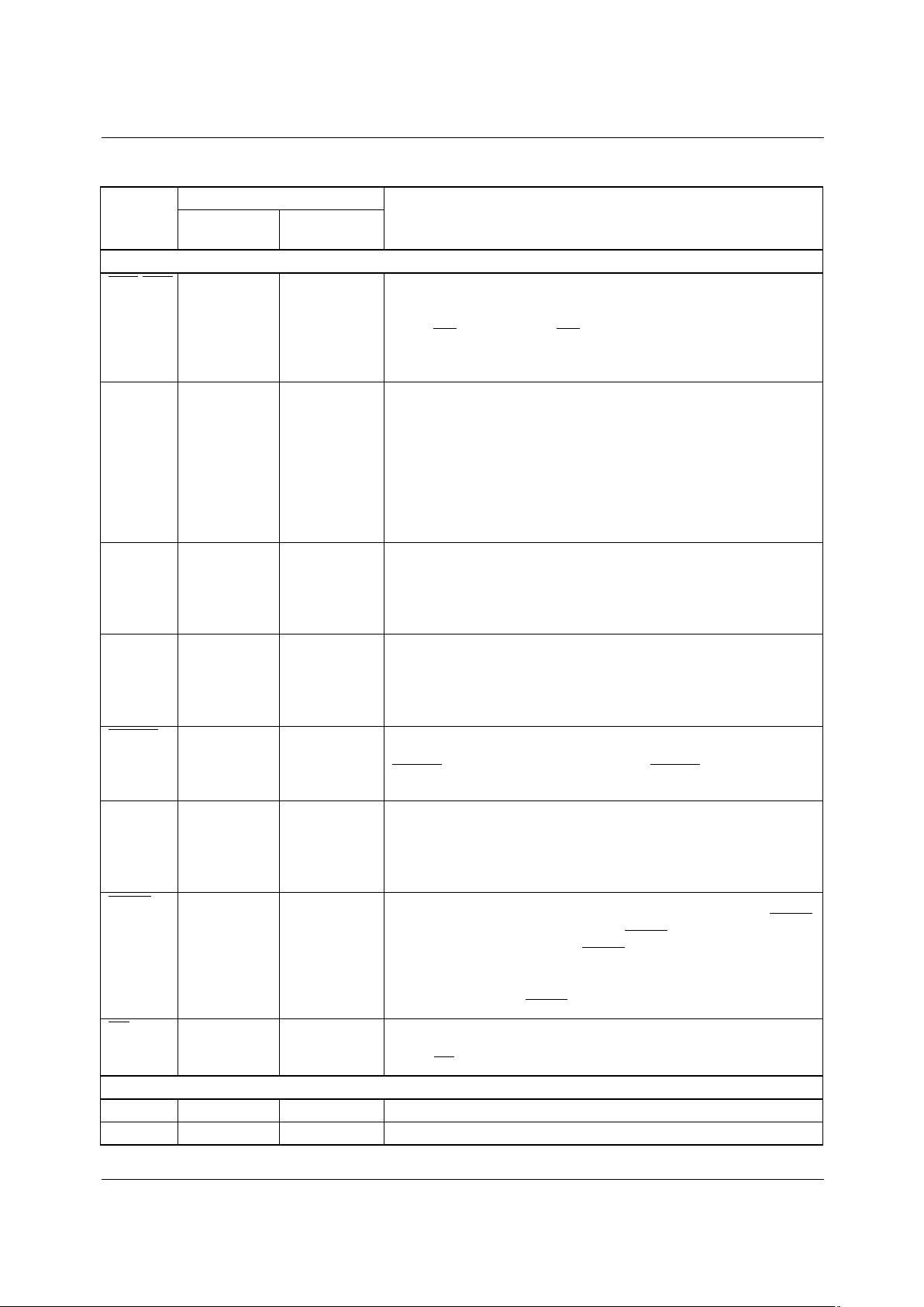
Pin Descriptions
Pin Name
Pin Number
Pin Function Description
CPGA/PPGA/
MPGA
MQFP
Power
V
DD
F3, H3, L7, C8 12, 20, 46, 102 Supply Voltage. The TMC2249A operates from a single +5V
supply. All power and ground pins must be connected.
GND E3, G3, J3, L6,
H11, C7
8, 16, 24, 42,
72, 106
Ground. The TMC2249A operates from a single +5V supply. All
power and ground pins must be connected.
Clock
CLK C3 1
System Clock. The TMC2249A operates from a single master
clock input. The rising edge of clock strobes all enabled registers.
All timing specifications are referenced to the rising edge of CLK.
Inputs
A
11-0
N8, M8, L8,
N9, M9, N10,
L9, M10, N11,
N12, L10, M11
48, 49, 50, 51,
52, 53, 54, 55,
56, 57, 58, 59
A-D Input. A through D are the four 12-bit registered data input
ports. A
0
-D
0
are the LSBs (see Table 1). Data presented to the input
ports is clocked in to the top of the 16-stage delay pipeline on the
next clock when enabled, "pushing" data down the register stack.
B
11-0
N7, M7, N6,
M6, N5, M5,
N4, L5, M4,
N3, M3, L4
47, 45, 44, 43,
41, 40, 39, 38,
37, 36, 35, 34
C
11-0
A9, B9, A10,
C9, B10, A11,
B11, C10, A12,
B12, C11, A13
101, 100, 99,
98, 97, 96, 95,
94, 93, 92, 91,
90
D
11-0
B8, A8, B7, A7,
A6, B6, C6, A5,
B5, A4, C5, B4
103, 104, 105,
107, 108, 109,
110, 111, 112
113, 114, 115
ADEL
3-0
L11, M12,
M13, K11
61, 62, 63, 64 A-D Delay. ADEL through DDEL are the four-bit registered input
data pipe delay select word inputs. Data to be presented to the
multipliers is selected from one of sixteen stages in the input data
delay pipe registers, as indicated by the delay select word
presented to the respective input port during that clock. The
minimum delay is one clock (select word=0000), and the maximum
delay is 16 clocks (select word=1111). Following powerup these
values are indeterminate and must be initialized by the user.
BDEL
3-0
M2, L3, N1, L2 32, 31, 30, 29
CDEL
3-0
D11, B13,
C13, D12
88, 87, 86, 85
DDEL
3-0
A2, C4, B3, A1 117, 118, 119,
120
CAS
15-0
L13, K12, J11,
K13, J12, J13,
H12, H13,
G12, G11,
G13, F13, F12,
F11, E13, E12
66, 67, 68, 69,
70, 71, 73, 74,
75, 76, 77, 78,
79, 80, 81, 82
Cascade Input. CAS is the 16-bit Cascade data input port. CAS
0
is
the LSB. See Table 1.
Controls
S
15-0
C1, D2, D1,
E2, E1, F2, F1,
G2, G1, H1,
H2, J1, J2, K1,
K2, L1
6, 7, 9, 10, 11,
13, 14, 15, 17,
18, 19, 21, 22,
23, 25, 26
Sum Output. The current 16-bit result is available at the Sum
output. The output may be the most or least significant 16 bits of the
current accumulator output, as determined by SWAP. S
0
is the LSB.
See Table 1.
PRODUCT SPECIFICATION TMC2249A
6
REV. 1.0.2 7/6/00
Controls
ENA
-END N13, N2, C12, A360, 33, 89, 116 Input Enables. Input data presented to port i11-0 (i=A,B,C, or D)
are latched into delay pipeline i, and data already in pipeline i
advance by one register position, on each rising edge of CLK for
which ENi
is LOW. When ENi is HIGH, the data in pipeline i do not
move and the value at the input port i will be lost before it reaches
the multiplier.
NEG1,2 B1, D3 3, 4
Negate. The products of the multipliers are negated causing a
subtraction to be performed during the internal summation of
products, when the NEGate controls are HIGH, NEG1 negates the
product A x B, while NEG2 acts on the output of the multiplier which
generates the product C x D. When the length controls ADEL–
DDEL are set to zero, these controls indicate the operation to be
performed on data input during the same clock. As nonzero values
for ADEL–DDEL do not affect the pipelining of these controls, their
effect is not synchronous with the data input in these cases.
RND C2 5
Round. When the rounding control is HIGH, the 24-bit sum of
products resulting from data input during that clock is rounded to 16
bits. When enabled rounding is automatically performed only during
the first cycle of each accumulation sequence, to avoid the
accumulation of roundoff errors.
FT E11 84
Feedthrough. When the Feedthrough control is HIGH, the pipeline
delay through the cascade data path is minimized to simplify the
cascading of multiple devices. When FT is LOW and ADEL through
DDEL are all set to 0, the data inputs are aligned, such that
S(n+6) = CAS(n) + A(n)B(n) + C(n)D(n). See Table 2.
CASEN
D13 83
Cascade Enable. Data presented at the cascade data input port
are latched and accumulated internally when the input enable
CASEN during that clock is LOW. When CASEN is HIGH, the
cascade input port is ignored.
ACC B2 2
Accumulate. When the registered ACCumulator control is LOW, no
internal accumulation will be performed on the data input during the
current clock, effectively clearing the prior accumulated sum. When
ACC is HIGH, the internal accumulator adds the emerging product
to the sum of the previous products and RND is disabled.
SWAP K3 28
Swap Output Words. The user may access both the most and
least-significant 16 bits of the 24-bit accumulator by utilizing SWAP.
Normal operation of the device, with SWAP = HIGH, outputs the
most significant word. Setting SWAP = LOW puts a double-register
structure into "toggle" mode, allowing the user to examine the LSW
on alternate clocks. New output data will not be clocked into the
output registers until SWAP returns HIGH.
OE M1 27
Output Enable. Data currently in the output registers is available at
the output bus S
15-0
when the asynchronous Output Enable is LOW.
When OE is HIGH, the outputs are in the high-impedance state.
No Connect
L12 65 Do Not Connect
D4 Index Pin (optional)
Pin Descriptions
(continued)
Pin Name
Pin Number
Pin Function Description
CPGA/PPGA/
MPGA
MQFP
 Loading...