

Fairchild Semiconductor TMC2246AX1 Datasheet
www.fairchildsemi.com
REV. 1.0.3 9/11/00
Features
• 60 MHz computation rate
• 60 MHz data and coefficient input
• Four 11 x 10-bit multipliers
• Individual data and coefficient inputs
• 25-Bit accumulator
• Fractional and integer two’s complement data formats
• Input and output data latches with user-configurable
enables
• Selectable 16-bit rounded output
• Internal 1/2 LSB rounding
• Available in 120-pin CPGA, PPGA, MPGA, or MQFP
Applications
• Fast pixel interpolation
• Fast image manipulation
• Image mixing and keying
• High-performance FIR filters
• Adaptive digital filters
• One- and two-dimensional image processing
Description
The TMC2246A is a video-speed convolutional array composed of four 11 x 10 bit registered multipliers followed by a
summer and an accumulator. All eight multiplier inputs are
accessible to the user and may be updated every clock cycle
with integer or fractional two’s complement data. A pipelined architecture, fully registered input and output ports,
and asynchronous three-state output enable control simplify
the design of complex systems.
The data or coefficient inputs to the multipliers may be held
over multiple clock cycles, providing storage for mixing and
filtering coefficients. The 25-bit internal accumulator path
allows two bits of cumulative word growth and may be internally rounded to 16 bits. Output data are updated every clock
cycle, or may be held under user control. All data inputs, outputs, and controls are TTL compatible and (except for the
three-state output enable) are registered on the rising edge of
CLK.
The TMC2246A is uniquely suited to performing pixel interpolation in image manipulation and filtering applications. As
a companion to the Fairchild Semiconductor TMC2301 and
TMC2302 Image Manipulation Sequencers, the TMC2246A
can execute a bilinear interpolation of an image (4-pixel kernels) at real-time video rates. Larger kernels or other, more
complex, functions can be realized with no loss in performance
by utilizing multiple devices.
With unrestricted access to all data and coefficient input
ports, the TMC2246A offers considerable flexibility in applications performing digital filtering, adaptive FIR filters, mixers, and other similar systems requiring high-speed
processing.
Fabricated in a submicron CMOS process, the TMC2246A
operates at a guaranteed clock rate of 60 MHz over the full
temperature and supply voltage ranges. It is pin- and function-compatible with Fairchild’s TMC2246, while providing
higher speed operation and lower power dissipation. It is
available in a 120 pin Plastic Pin Grid Array (PPGA), 120
pin Ceramic Pin Grid Array (CPGA), 120 lead MQFP to
PPGA (MPGA), and a 120 lead Metric Quad FlatPack
(MQFP).
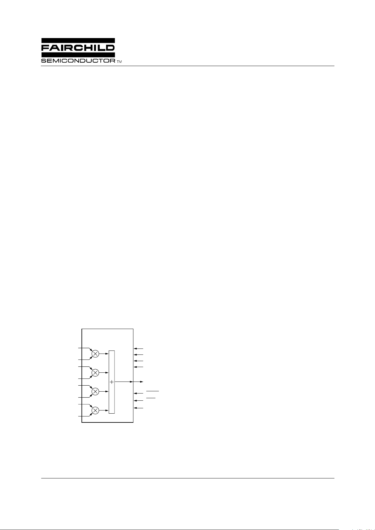
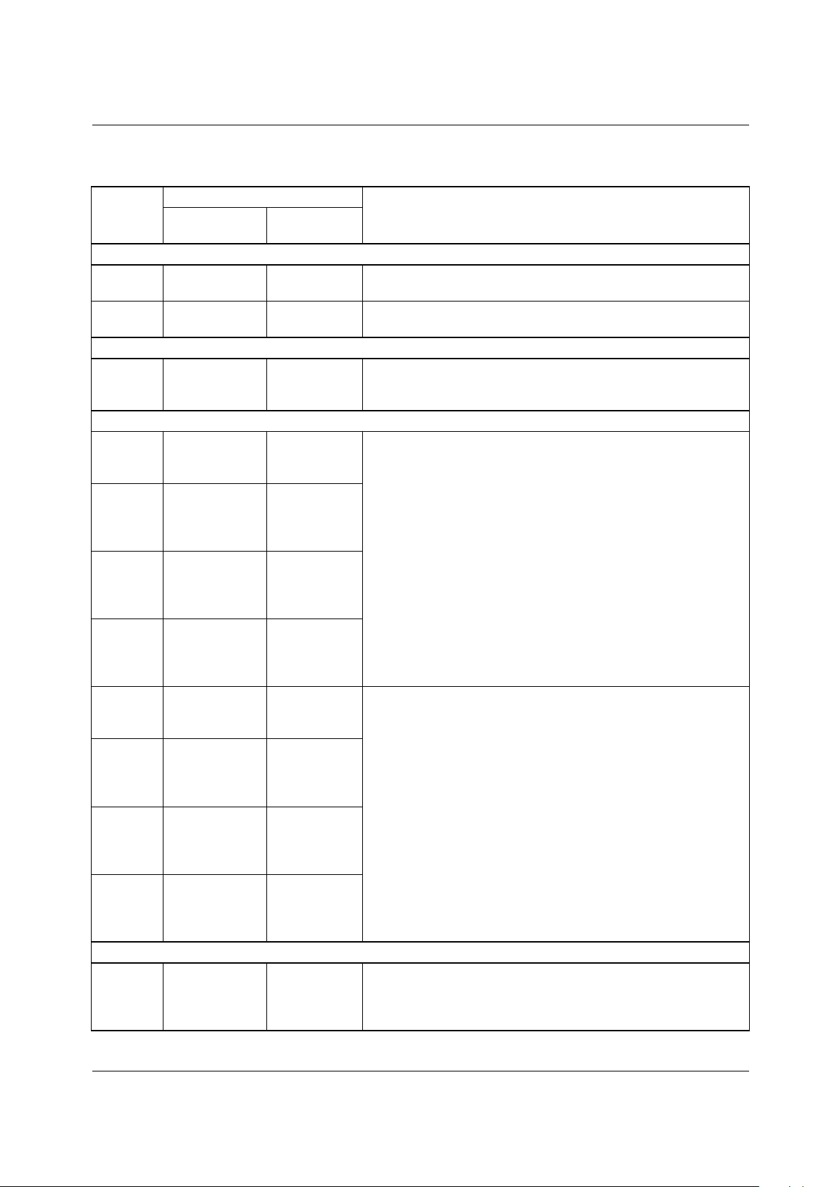
Logic Symbol
D1
9-0
D2
9-0
D3
9-0
D4
9-0
ENB1-4
ENSEL
ACC
FSEL
OCEN
OEN
CLK
TMC2246A
Image Filter
C1
10-0
C2
10-0
C3
10-0
C4
10-0
S
15-0
TMC2246A
Image Filter
11 x 10 bit, 60 MHz
PRODUCT SPECIFICATION TMC2246A
2
REV. 1.0.3 9/11/00
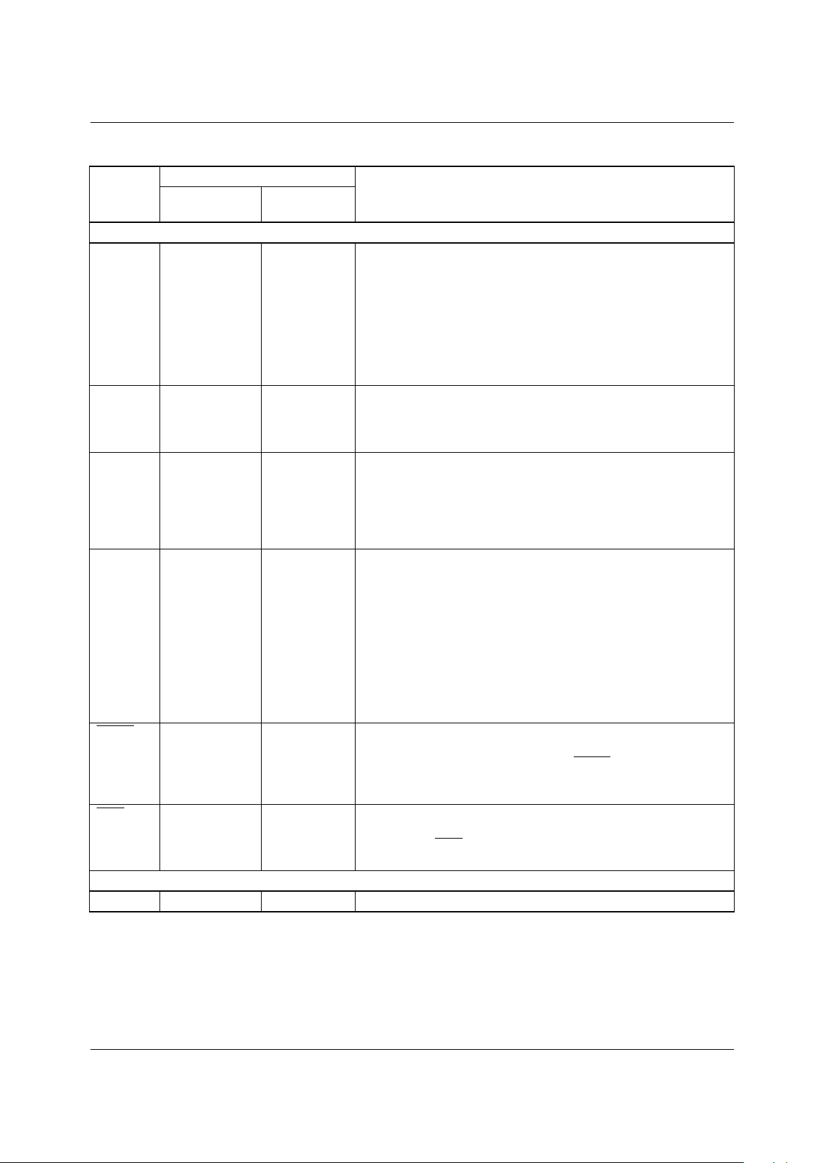
Block Diagram
ENB2D1
9-0
D2
9-0
D3
9-0
D4
9-0
C1
10-0
C2
10-0
C3
10-0
C4
10-0
ENB1
ENSEL
ACC
FSEL
*
*Automatic rounding function
OCEN
OEN
S
15-0
ENB3 ENB4
CLK
25
2
-10
LSB MSB
Functional Description
The TMC2246A Image Filter is a flexible multiplier-summer
array which computes the accumulated sum of four 11x10
bit products, allowing word growth up to 25 bits.
The inputs are user-configurable, allowing latching of either
the 10- or 11-bit input data. The data format is user-selectable
between integer or fractional two’s complement arithmetic.
Total latency from input registers to output data port is 5
clocks.
The output data path is 16 bits wide, providing the lower 16
bits of the accumulator when in integer format or the upper
16 bits of the 25-bit accumulator path when fractional two’s
complement notation is selected. One-time rounding to 16
bits is performed automatically when accumulating fractional data, but is disabled when operating in integer format
to maintain the integrity of the least-significant bits.
TMC2246A PRODUCT SPECIFICATION
REV. 1.0.3 9/11/00
3
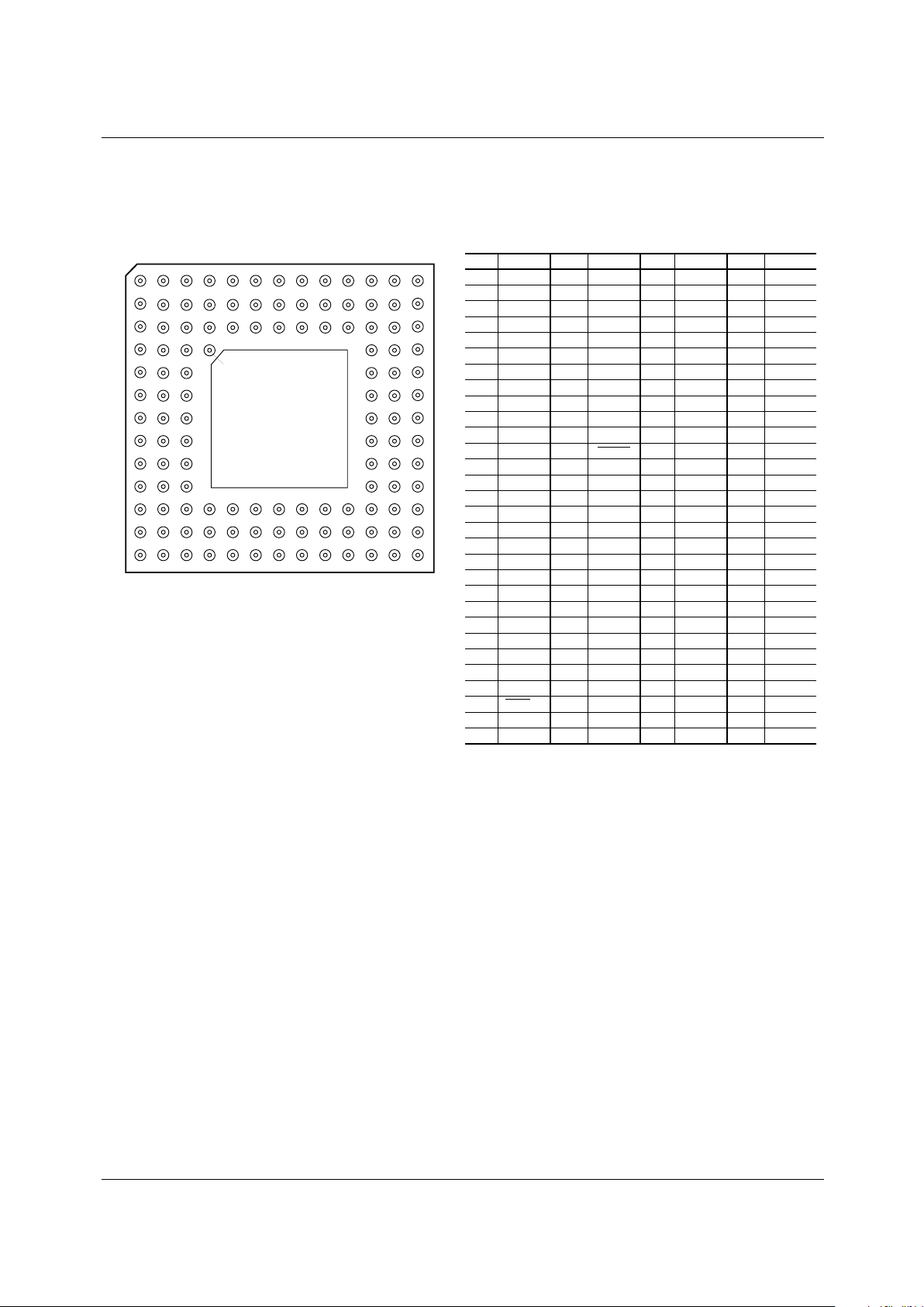
Pin Assignments
120 Pin Plastic Pin Grid Array, H5 Package, 120 Pin Ceramic Pin Grid Array, G1 Package, and
120 Pin Metric Quad FlatPack to 120 Pin Plastic Pin Array, H6 Package
B
A
D
E
F
G
H
J
K
L
M
N
C
12345678910111213
ENSEL
ENB2
ENB3
D4
7
D4
5
D4
2
D4
1
C4
10
C4
8
C4
6
C4
3
C4
0
C3
2
ACC
FSEL
ENB4
D4
9
D4
6
D4
3
D4
0
C4
9
C4
7
C4
4
C4
2
C3
0
C3
5
S
15
OEN
CLK
ENB1
A1
A2
A3
A4
A5
A6
A7
A8
A9
A10
A11
A12
A13
B1
B2
B3
B4
B5
B6
B7
B8
B9
B10
B11
B12
B13
C1
C2
C3
C4
D4
8
D4
4
GND
V
DD
C4
5
C4
1
C3
1
C3
3
C3
6
S
13
S
14
OCEN
C3
4
C3
7
C3
9
S
11
S
12
GND
C3
8
C3
10
D3
0
S
9
S
10
V
DD
D3
1
D3
2
D3
3
S
7
S
8
GND
C5
C6
C7
C8
C9
C10
C11
C12
C13
D1
D2
D3
D11
D12
D13
E1
E2
E3
E11
E12
E13
F1
F2
F3
F11
F12
F13
G1
G2
G3
Pin Name Pin Name
D3
5
D3
6
D3
4
S
6
S
5
V
DD
GND
D3
8
D3
7
S
4
S
3
GND
D2
7
D2
9
D3
9
S
2
S
1
D1
8
D2
3
D2
6
D2
8
S
0
D1
7
D1
5
D1
2
C1
9
GND
V
DD
C2
0
C2
4
G11
G12
G13
H1
H2
H3
H11
H12
H13
J1
J2
J3
J11
J12
J13
K1
K2
K3
K11
K12
K13
L1
L2
L3
L4
L5
L6
L7
L8
L9
C2
8
D2
0
D2
4
D2
5
D1
9
D1
4
D1
1
C1
10
C1
7
C1
5
C1
3
C1
0
C2
2
C2
5
C2
9
D2
1
D2
2
D1
6
D1
3
D1
0
C1
8
C1
6
C1
4
C1
2
C1
1
C2
1
C2
3
C2
6
C2
7
C2
10
L10
L11
L12
L13
M1
M2
M3
M4
M5
M6
M7
M8
M9
M10
M11
M12
M13
N1
N2
N3
N4
N5
N6
N7
N8
N9
N10
N11
N12
N13
Pin Name Pin Name
Top View
Cavity Up
KEY
PRODUCT SPECIFICATION TMC2246A
4
REV. 1.0.3 9/11/00
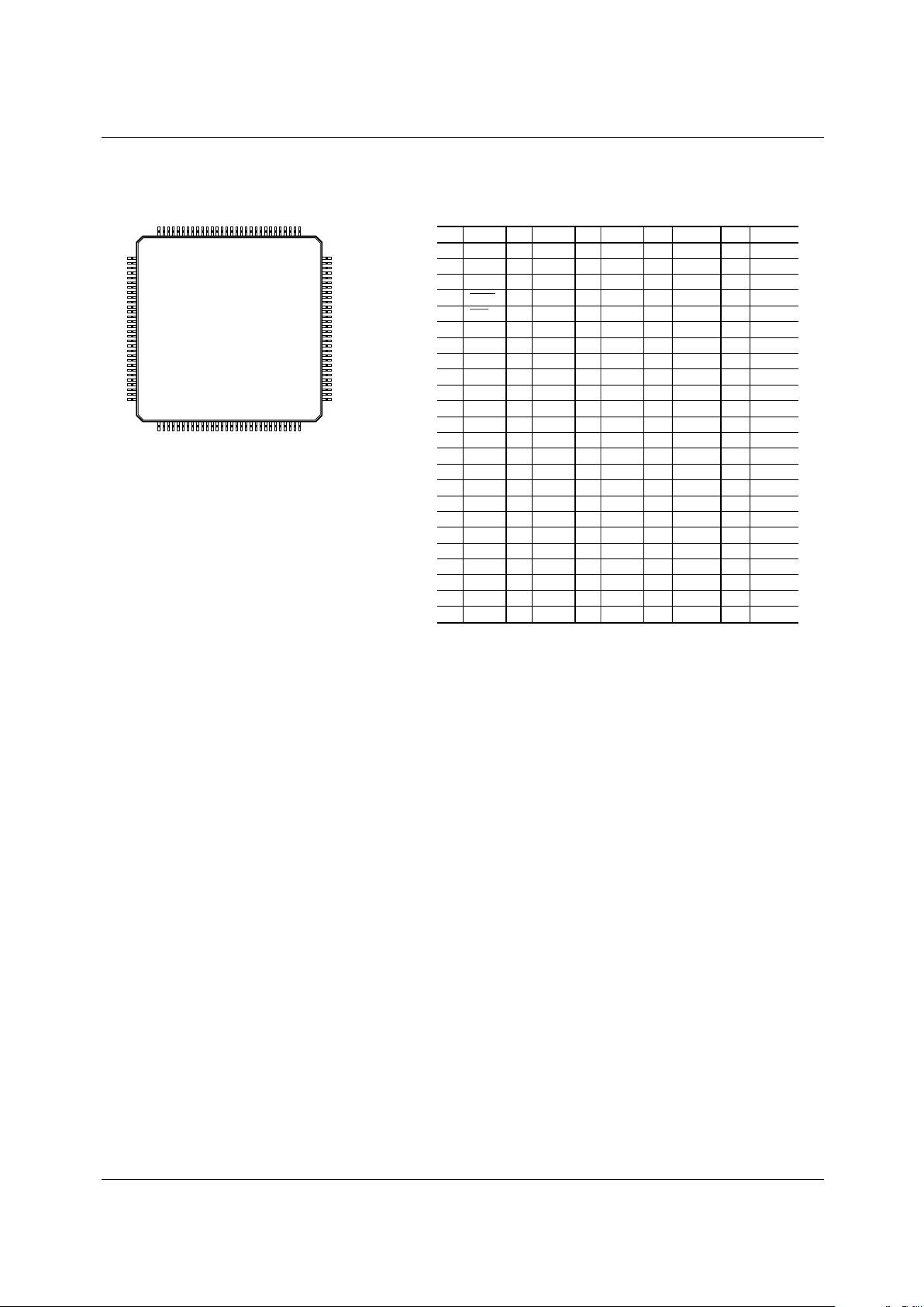
Pin Assignments
120 Lead Metric Quad Flat Pack (KE) Package
C4
4
C4
5
C4
6
C4
7
C4
8
V
DD
C4
9
C4
10
D4
0
GND
D4
1
D4
2
D4
3
D4
4
D4
5
D4
6
D4
7
D4
8
D4
9
ENB3
ENB2
ENB1
ENB4
ENSEL
97
98
99
100
101
102
103
104
105
106
107
108
109
110
111
112
113
114
115
116
117
118
119
120
Pin Name
CLK
FSEL
ACC
OCEN
OEN
S
15
S
14
GND
S
13
S
12
S
11
V
DD
S
10
S
9
S
8
GND
S
7
S
6
S
5
V
DD
S
4
S
3
S
2
GND
1
120
1
2
3
4
5
6
7
8
9
10
11
12
13
14
15
16
17
18
19
20
21
22
23
24
S
1
S
0
D1
9
D1
8
D1
7
D1
6
D1
5
D1
4
D1
3
D1
2
D1
1
D1
0
C1
10
C1
9
C1
8
C1
7
C1
6
GND
C1
5
C1
4
C1
3
V
DD
C1
2
C1
1
25
26
27
28
29
30
31
32
33
34
35
36
37
38
39
40
41
42
43
44
45
46
47
48
Pin Name Pin Name
C1
0
C2
0
C2
1
C2
2
C2
3
C2
4
C2
5
C2
6
C2
7
C2
8
C2
9
C2
10
D2
0
D2
1
D2
2
D2
3
D2
4
D2
5
D2
6
D2
7
D2
8
D2
9
D3
9
GND
49
50
51
52
53
54
55
56
57
58
59
60
61
62
63
64
65
66
67
68
69
70
71
72
D3
8
D3
7
D3
6
D3
5
D3
4
D3
3
D3
2
D3
1
D3
0
C3
10
C3
9
C3
8
C3
7
C3
6
C3
5
C3
4
C3
3
C3
2
C3
1
C3
0
C4
0
C4
1
C4
2
C4
3
73
74
75
76
77
78
79
80
81
82
83
84
85
86
87
88
89
90
91
92
93
94
95
96
Pin Name Pin Name
TMC2246A PRODUCT SPECIFICATION
REV. 1.0.3 9/11/00
5
Pin Descriptions
Pin Name
Pin Number
Pin Function Description
CPGA/PPGA/
MPGA
MQFP
Power
V
DD
F3, H3, L7, C8 12, 20, 46, 102 Supply Voltage. The TMC2246A operates from a single +5V
supply. All power and ground pins must be connected.
GND E3, G3, J3, L6,
H11, C7
8, 16, 24, 42,
72, 106
Ground. The TMC2246A operates from a single +5V supply. All
power and ground pins must be connected.
Clock
CLK C3 1
System Clock. The TMC2246A operates from a single master
clock input. The rising edge of clock strobes all enabled registers.
All timing specifications are referenced to the rising edge of CLK.
Inputs
D1
9-0
M1, K3, L2, N1,
L3, M2, N2, L4,
M3, N3
27, 28, 29, 30,
31, 32, 33, 34,
35, 36
Data Input Ports. D1 through D4 are the 10-bit data input ports.
The LSB is Dx
0
.
D2
9-0
J12, K13, J11,
K12, L13, L12,
K11, M13, M12,
L11
70, 69, 68, 67,
66, 65, 64, 63,
62, 61
D3
9-0
J13, H12, H13,
G12, G11, G13,
F13, F12, F11,
E13
71, 73, 74, 75,
76, 77, 78, 79,
80, 81
D4
9-0
B4, C5, A4, B5,
A5, C6, B6, A6,
A7, B7
115, 114, 113,
112, 111, 110,
109, 108, 107,
105
C1
10-0
M4, L5, N4, M5,
N5, M6, N6, M7,
N7, N8, M8
37, 38, 39, 40,
41, 43, 44, 45,
47, 48, 49
Coefficient Input Ports. C1 through C4 are the 11-bit coefficient
input ports. The LSB is Cx
0
.
C2
10-0
N13, M11, L10,
N12, N11, M10,
L9, N10, M9,
N9, L8
60, 59, 58, 57,
56, 55, 54, 53,
52, 51, 50
C3
10-0
E12, D13, E11,
D12, C13, B13,
D11, C12, A13,
C11, B12
82, 83, 84, 85,
86, 87, 88, 89,
90, 91, 92
C4
10-0
A8, B8, A9, B9,
A10, C9, B10,
A11, B11, C10,
A12
104, 103, 101,
100, 99, 98, 97,
96, 95, 94, 93
Outputs
S
15-0
C1, D2, D1, E2,
E1, F2, F1, G2,
G1, H1, H2, J1,
J2, K1, K2, L1
6, 7, 9, 10, 11,
13, 14, 15, 17,
18, 19, 21, 22,
23, 25, 26
Sum Output. The current 16-bit result is available at the Sum
output. The LSB is S
0
. See the Functional Block Diagram .
PRODUCT SPECIFICATION TMC2246A
6
REV. 1.0.3 9/11/00
Note:
1. X denotes a "Don't Care" condition.
2. Any register not explicitly held is updated on the next rising edge of CLK.
Controls
FSEL B2 2
Format Select. Coefficients input during the current clock are
assumed to be in fractional two's complement format. Rounding to
16 bits is performed as determined by the accumulator control,
ACC, and the upper 16 bits of the accumulator are output when
the registered Format Select input (FSEL) is LOW. When FSEL is
HIGH, two's complement integer format is assumed, and the
lower 16 bits of the accumulator are presented at the output. No
rounding is performed when operating in integer mode. See the
Functional Block Diagram and the Applications Discussion.
ENSEL A1 120
Enable Select. The registered Enable Select determines whether
the data or the coefficient input registers may be held on the next
rising edge of clock, in conjunction with the individual input
enables ENB1–ENB4. See Table 1.
ENB1–
ENB4
C4, A2, A3, B3 118, 117, 116,
119
Input Enables. When ENBi (i=1, 2, 3, or 4) is LOW, registers Ci
and Di are both strobed by the next rising edge of CLK. When
ENBi is HIGH and ENSEL is LOW, Di is strobed, but Ci is held.
When ENBi and ENSEL are both HIGH, Di is held and Ci is
strobed. See Table 1. Thus, either or both input registers to each
multiplier are updated on each clock cycle.
ACC B1 3
Accumulate. When the registered ACCumulator control is LOW,
no internal accumulation will be performed on the data input
during the current clock, effectively clearing the prior accumulated
sum. If operating in fractional two's complement format (FSEL =
LOW), one-half LSB rounding to 16 bits is performed on the result.
This allows the user to perform summations without propagating
roundoff errors.
When ACC is HIGH, the internal accumulator adds the emerging
products to the sum of previous products, without performing
additional rounding.
OCEN
D3 4
Output Register Enable. The output of the accumulator is
latched into the output register on the next clock when the Output
Register Clock Enable is LOW. When OCEN is HIGH the contents
of the output register remain unchanged; however, accumulation
will continue internally if ACC remains HIGH.
OEN
C2 5
Output Enable. Data currently in the output registers is available
at the output bus S
15-0
when the asynchronous Output Enable is
LOW. When OEN
is HIGH, the outputs are in the high-impedance
state.
No Connect
NC D4 (Index Pin) Not Connected. (Optional)
Pin Descriptions
(continued)
Pin Name
Pin Number
Pin Function Description
CPGA/PPGA/
MPGA
MQFP
 Loading...