

Fairchild Semiconductor SPT7830 Datasheet
SPT7830
A
A
10-BIT, 2.5 MSPS, SERIAL OUTPUT A/D CONVERTER
FEATURES
• 10-Bit, 1 kHz to 2.5 MSPS Analog-to-Digital Converter
• Monolithic CMOS
• Serial Output
• Internal Sample-and-Hold
• Analog Input Range: 0 to 2 V Nominal; 3.3 V Max
• Power Dissipation (Excluding Reference Ladder)
45 mW at +5 V
16 mW at +3.0 V
• Single Power Supply: +3 V to +5 V Range
• High ESD Protection: 3,000 V Minimum
GENERAL DESCRIPTION
The SPT7830 10-bit, 2.5 MSPS, serial analog-to-digital
converter delivers excellent high speed conversion performance with low cost and low power. The serial port protocol
is compatible with the serial peripheral interface (SPI) or
MICROWIRE™ industry standard, high-speed synchronous
MPU interfaces. The large input bandwidth and fast transient
response time allow for CCD applications operating up to
2.5 MSPS.
APPLICATIONS
• Handheld and Desktop Scanners
• DSP Interface Applications
• Portable Digital Radios
• Portable and Handheld Applications
• Automotive Applications
• Remote Sensing
The device can operate with a power supply range from
+3 V to +5 V with very low power dissipation. The small
package size makes this part excellent for hand-held applications where board space is at a premium. The SPT7830 is
available in an 8-lead SOIC package over the commercial
and industrial temperature ranges. Contact the factory for
availability of die.
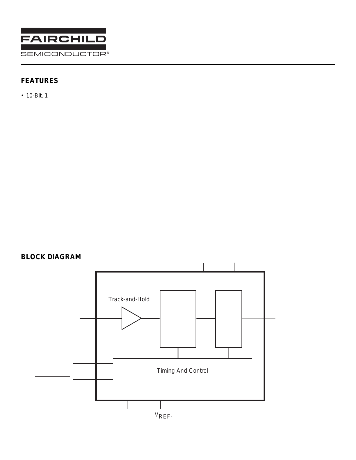
BLOCK DIAGRAM
Analog Input
Clock
Start Convert
Ground
Track-and-Hold
SAR
10-Bit
A/D
AAAAAAAAAAAAAAA
Timing And Control
AAAAAAAAAAAAAAA
V
REF+
V
REF-
V
Serial
Output
Logic
DD
Data Out

ABSOLUTE MAXIMUM RATING (Beyond which damage may occur)
1
Supply Voltages
VDD...........................................................................+6 V
Input Voltages
Analog Input ................................................ –0.7 to +6 V
V
+ .......................................................... –0.7 to +6 V
REF
V
– .......................................................... –0.7 to +6 V
REF
Clock and SC.............................................. –0.7 to +6 V
Output
Data Out ................................................................10 mA
Temperature
Operating, ambient ...............................–40 to +85 °C
junction......................................... +175 °C
Lead, Soldering (10 seconds) ............................ +300 °C
Storage ....................................................–65 to +150 °C
Note: 1. Operation at any Absolute Maximum Ratings is not implied. See Electrical Specifications for proper nominal applied
conditions in typical applications.
ELECTRICAL SPECIFICATIONS
TA = +25 °C, VDD = +5.0 V, VIN = 0 to +3 V, f
PARAMETERS CONDITIONS LEVEL MIN TYP MAX UNITS
DC ELECTRICAL CHARACTERISTICS
DC Performance
Resolution 10 Bits
Differential Linearity VI ±0.5 ±1.0 LSB
Integral Linearity VI ±1.0 ±1.5 LSB
No Missing Codes VI Guaranteed
Analog Input
Input Voltage Range
Input Resistance VI 5 MΩ
Input Capacitance IV 5 pF
Input Bandwidth (Small Signal) IV 30 MHz
Offset IV –2 +2 % of FSR
Gain Error IV –2 +2 % of FSR
Reference Input
Resistance IV 250 280 350 Ω
Voltage Range
2
V
–
REF
2
V
+
REF
V
– V
REF+
REF–
Reference Settling Time IV 90 ns
Timing Characteristics
Maximum Conversion Rate VI 2.5 1.0 MSPS
Minimum Conversion Rate IV 1 kSPS
Maximum External Clock Rate VI 35 14 MHz
Minimum External Clock Rate IV 14 kHz
Aperture Delay Time IV 5 ns
Aperture Jitter Time IV 5 ps
Data Output LSB Hold Time T
1
Percentages refer to percent of [(V
2
∆ = Minimum (V
1
1
(∆) IV 1/10 V
– V
REF+
REF
–)
= 35 MHz, fS = 2.5 MSPS, V
CLK
TEST TEST
to T
REF
MIN
+) – (V
REF
MAX
–)]
+ = +3.0 V, V
REF
IV V
REF
IV –4% 0 V
IV V
REF–
– = 0.0 V, unless otherwise specified.
REF
– +4% V
+∆ 2/3 V
DD
REF+
REF+
–6% V
–∆ V
DD
IV 6 8 ns
V
V
SPT7830
2 12/29/99

ELECTRICAL SPECIFICATIONS
TA = +25 °C, VDD = +5.0 V, VIN = 0 to +3 V, f
PARAMETERS CONDITIONS LEVEL MIN TYP MAX UNITS
Dynamic Performance
Effective Number of Bits
f
= 500 kHz IV 8.9 Bits
IN
= 1 MHz IV 8.5 Bits
f
IN
Signal-to-Noise Ratio
fIN = 500 kHz IV 56 dB
= 1 MHz IV 55 dB
f
IN
Harmonic Distortion
fIN = 500 kHz IV 63 dB
fIN = 1 MHz IV 58 dB
Power Supply Requirements
+V
Supply Voltage IV 3 5.5 V
DD
Supply Current VDD = +3.0 V IV 5.4 7 mA
+V
DD
Power Dissipation
3
Excluding reference ladder.
3
= 35 MHz, fS = 2.5 MSPS, V
CLK
TEST TEST
= +5.0 V VI 9 10 mA
V
DD
VDD = +3.0 V IV 16 22 mW
VDD = +5.0 V VI 45 50 mW
+ = +3.0 V, V
REF
– = 0.0 V, unless otherwise specified.
REF
TEST LEVEL CODES
All electrical characteristics are subject to the
following conditions:
All parameters having min/max specifications
are guaranteed. The Test Level column indicates the specific device testing actually performed during production and Quality Assurance inspection. Any blank section in the data
column indicates that the specification is not
tested at the specified condition.
TEST LEVEL
I
II
III
IV
V
VI
TEST PROCEDURE
100% production tested at the specified temperature.
100% production tested at TA=+25 °C, and sample
tested at the specified temperatures.
QA sample tested only at the specified temperatures.
Parameter is guaranteed (but not tested) by design
and characterization data.
Parameter is a typical value for information purposes
only.
100% production tested at TA = +25 °C. Parameter is
guaranteed over specified temperature range.
SPT7830
3 12/29/99
 Loading...