

Fairchild Semiconductor SPT7725 Datasheet
SPT7725
8-BIT, 300 MSPS, FLASH A/D CONVERTER
TECHNICAL DATA
AUGUST 17, 2001
FEATURES
• Metastable errors reduced to 1 LSB
• Low input capacitance: 10 pF
• Wide input bandwidth: 210 MHz
• 300 MSPS conversion rate
• Typical power dissipation: 2.2 watts
GENERAL DESCRIPTION
The SPT7725 is a monolithic flash A/D converter capable
of digitizing a two volt analog input signal into 8-bit digital
words at a 300 MSPS (typ) update rate.
For most applications, no external sample-and-hold is required for accurate conversion due to the device’s narrow
aperture time, wide bandwidth, and low input capacitance.
A single standard –5.2 volt power supply is required for
operation of the SPT7725, with nominal power dissipation
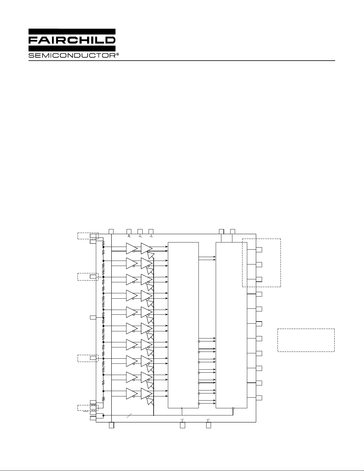
BLOCK DIAGRAM
V
RTS
V
RTF
Analog Input
(Force or Sense)
AGND DGND V
Preamp Comparator
256
255
EE
Clock
Buffer
APPLICATIONS
• Digital oscilloscopes
• Transient capture
• Radar, EW, ECM
• Direct RF down-conversion
• Medical electronics: ultrasound, CAT instrumentation
of 2.2 W. A proprietary decoding scheme reduces meta-
stable errors to the 1 LSB lev el.
The SPT7725 is available in 42-lead ceramic sidebrazed
DIP, surface-mount 44-lead cerquad, and 46-lead PGA
packages (all are pin-compatible with the SPT7710); the
cerquad and PGA packages allow access to additional
reference ladder taps, an overrange bit, and a data ready
output. The SPT7725 is available in the industrial temperature range.
LINV MINV
DRINV
MSB D7
DREAD
Convert
V
V
V
V
V
RBF
RBS
CLK
CLK
R3
R2
R1
(Sense or Force)
152
151
128
256 to
127
64
63
2
1
2
8-Bit
Encoder
V
EE
D6
D5
D4
D3
D2
D1
LSB D0
AGNDAnalog Input
ECL
Latches
and
Buffers
Overrange
D7 MSB
D6
D5
These functions are
D4
available in the PGA and
cerquad packages only.
D3
D2
D1
D0 LSB

ABSOLUTE MAXIMUM RATINGS (Beyond which damage may occur)1 25 °C
Supply Voltages
Negative Supply Voltage (VEE TO GND) –7.0 to +0.5 V
Ground Voltage Differential ....................–0.5 to +0.5 V
Input Voltage
Analog Input Voltage ...............................V
to +0.5 V
EE
Temperature
Operating Temperature,ambient............. –25 to +85 °C
junction ...................... +150 °C
Lead Temperature, (soldering 10 seconds) ..... +300 °C
Storage Temperature............................ –65 to +150 °C
Reference Input Voltage..........................VEE to +0.5 V
Digital Input Voltage ................................VEE to +0.5 V
Reference Current V
Output
Digital Output Current ............................... 0 to –30 mA
RTF
to V
........................25 mA
RBF
Note: 1. Operation at any Absolute Maximum Rating is not implied. See
Electrical Specifications for proper nominal applied conditions
in typical applications.
ELECTRICAL SPECIFICATIONS
TA= T
PARAMETERS CONDITIONS LEVEL MIN TYP MAX MIN TYP MAX UNITS
DC Accuracy
Analog Input
to T
MIN
, VEE=–5.2 V , R
MAX
Source
=50 Ω, V
=–2.00 V , VR2=–1.00 V , V
RBF
=0.00 V , ƒ
RTF
=250 MHz, Duty Cycle=50%, unless otherwise specified.
CLK
TEST TEST SPT7725A SPT7725B
Integral Linearity Error ƒ
Differential Linearity Error ƒ
= 100 kHz VI –0.75 ±0.60 +0.75 –0.95 ±0.80 +0.95 LSB
CLK
= 100 kHz VI –0.75 +0.75 –0.95 +0.95 LSB
CLK
No missing codes Guaranteed Guaranteed
Offset Error V
Offset Error V
RT
RB
VI –30 +30 –30 +30 mV
VI –30 +30 –30 +30 mV
Input Voltage Range VI –2.0 0.0 –2.0 0.0 Volts
Input Capacitance Over full
input range V 10 10 pF
Input Resistance V 15 15 kΩ
Input Current VI 250 500 250 500 µA
Input Slew Rate V 1,000 1,000 V/µs
Large Signal Bandwidth V
Small Signal Bandwidth V
=F.S. V 210 210 MHz
IN
=500 mV
IN
P-P
V 335 335 MHz
Clock Synchronous
Input Currents V 40 40 µA
Reference Input
Ladder Resistance VI 100 200 300 100 200 300 Ω
Reference Bandwidth V 10 10 MHz
Timing Characteristics
Maximum Sample Rate IV 250 300 250 300 MSPS
Clock to Data Delay V 2.4 2.4 ns
Output Delay Tempco V 2 2 ps/°C
CLK-to-Data Ready Delay (t
) V 2.0 2.0 ns
D
Aperture Jitter V 5 5 ps
Acquisition Time V 1.5 1.5 ns
Dynamic Performance
Signal-to-Noise Ratio ƒ
= 3.58 MHz VI 45 47 44 46 dB
IN
= 50 MHz VI 39 42 38 41 dB
ƒ
IN
Total Harmonic Distortion ƒIN = 3.58 MHz VI –52 –48 –50 –46 dB
= 50 MHz VI –43 –40 –42 –39 dB
ƒ
IN
Signal-to-Noise and Distortion ƒ
= 3.58 MHz VI 44 46 42 44 dB
IN
(SINAD) ƒIN = 50 MHz VI 37 39 35 37 dB
2 8/17/01
SPT7725

ELECTRICAL SPECIFICATIONS
TA= T
MIN
to T
MAX
, VEE=–5.2 V , R
Source
=50 Ω, V
=–2.00 V , VR2=–1.00 V , V
RBF
=0.00 V , ƒ
RTF
=250 MHz, Duty Cycle=50%, unless otherwise specified.
CLK
TEST TEST SPT7725A SPT7725B
PARAMETERS CONDITIONS LEVEL MIN TYP MAX MIN TYP MAX UNITS
Digital Inputs
Digital Input High Voltage
(MINV, LINV) VI –1.1 –0.7 –1.1 –0.7 Volts
Digital Input Low Voltage
(MINV, LINV) VI –2.0 –1.5 –2.0 –1.5 Volts
Clock Low Width, t
Clock High Width, t
PWL
PWH
VI 2.2 2.0 2 1.8 ns
VI 2.2 2.0 2 1.8 ns
Digital Outputs
Digital Output High Voltage 50 Ω to –2 V VI –1.1 –1.1 Volts
Digital Output Low Voltage 50 Ω to –2 V VI –1.5 –1.5 Volts
Power Supply Requirements
Supply Current +25 °C VI 425 550 425 550 mA
Power Dissipation +25 °C VI 2.2 2.9 2.2 2.9 W
TEST LEVEL CODES
All electrical characteristics are subject to the
following conditions:
All parameters having min/max specifications
are guaranteed. The Test Level column indicates the specific device testing actually performed during production and Quality Assurance inspection. Any blank section in the data
column indicates that the specification is not
tested at the specified condition.
LEVEL TEST PROCEDURE
I 100% production tested at the specified temperature.
II 100% production tested at TA = +25 °C, and sample tested at the
specified temperatures.
III QA sample tested only at the specified temperatures.
IV Parameter is guaranteed (but not tested) by design and characteri-
zation data.
V Parameter is a typical value for information purposes only.
VI 100% production tested at TA = +25 °C. Parameter is guaranteed
over specified temperature range.
Unless otherwise noted, all test are pulsed
tests; therefore, T
= TC = TA.
J
SPT7725
3 8/17/01
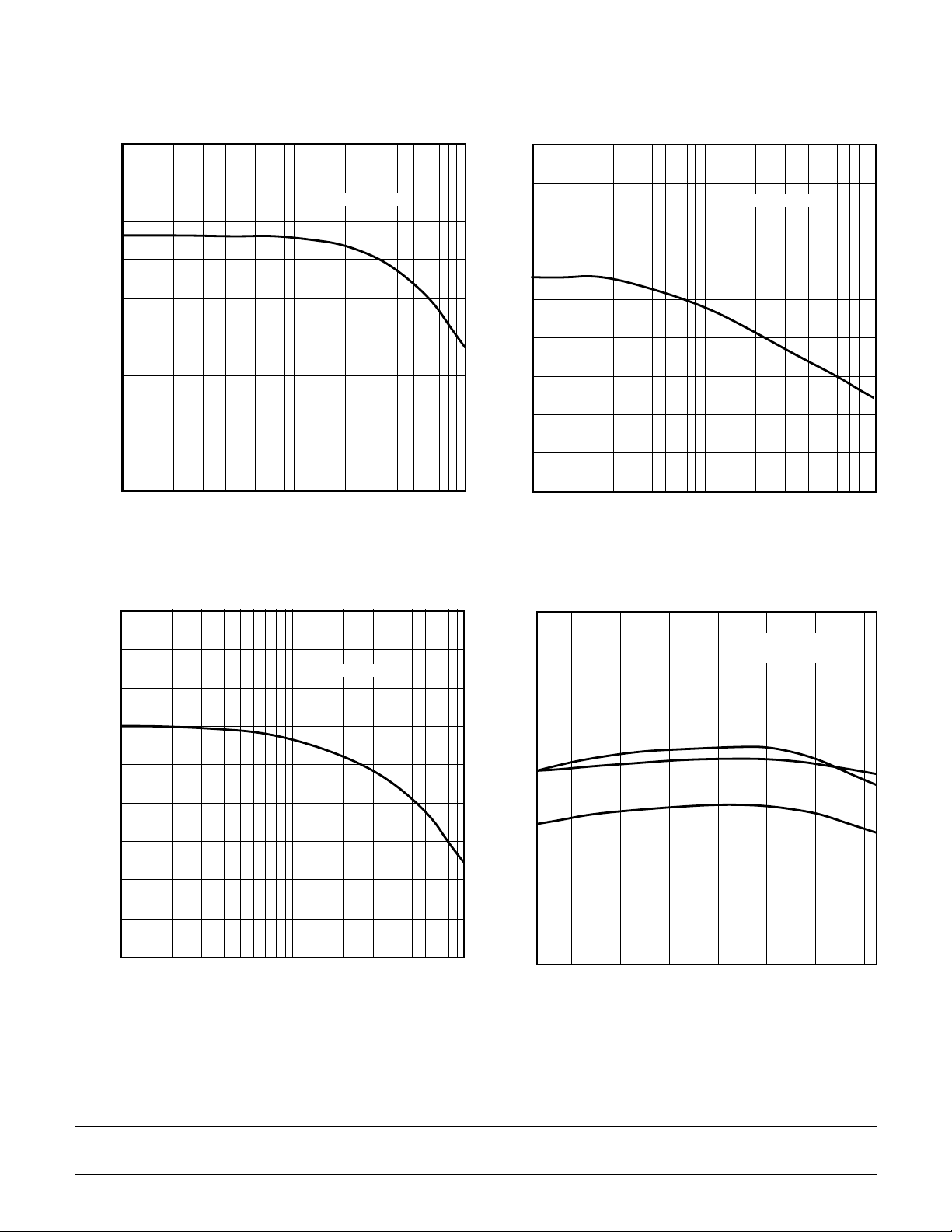
TYPICAL PERFORMANCE CHARACTERISTICS
SNR vs Input Frequency
52
50
S = 250 MSPS
48
46
44
42
40
Signal-to-Noise Ratio (dB)
38
36
34
1 10 100
Input Frequency (MHz)
THD vs Input Frequency
75
70
65
60
55
50
45
40
Total Harmonic Distortion (dB)
35
30
1 10 100
S = 250 MSPS
Input Frequency (MHz)
SINAD vs Input Frequency SNR, THD, SINAD vs Temperature
52
50
S = 250 MSPS
48
46
44
42
40
38
Signal-to-Noise and Distortion (dB)
36
34
1 10 100
Input Frequency (MHz)
50
45
40
SNR, THD, SINAD (dB)
35
30
40 20 0 20 40 60 80
Temperature (°C)
S = 250 MSPS
IN = 100 MHz
THD
SNR
SINAD
SPT7725
4 8/17/01
 Loading...