

Fairchild Semiconductor SPT5420 Datasheet
SPT5420
13-BIT, OCTAL D/A CONVER TER
TECHNICAL DATA
JUNE 26, 2001
FEATURES
• 13-bit resolution
• Pin compatible with AD7839
• Eight DACs in one package
• Buffered voltage outputs
• Wide output voltage swing VDD–2.5 V to VSS+2.5 V
• 15 µs settling time to ±0.5 LSB
• Double-buffered digital inputs
• Microprocessor and TTL/CMOS compatible
GENERAL DESCRIPTION
The SPT5420 contains eight 13-bit digital-to-analog
CMOS converters designed primarily for automatic test
equipment applications. It uses novel circuit topology to
convert the 13-bit digital inputs into output voltages which
are proportionate to the applied reference voltages. Each
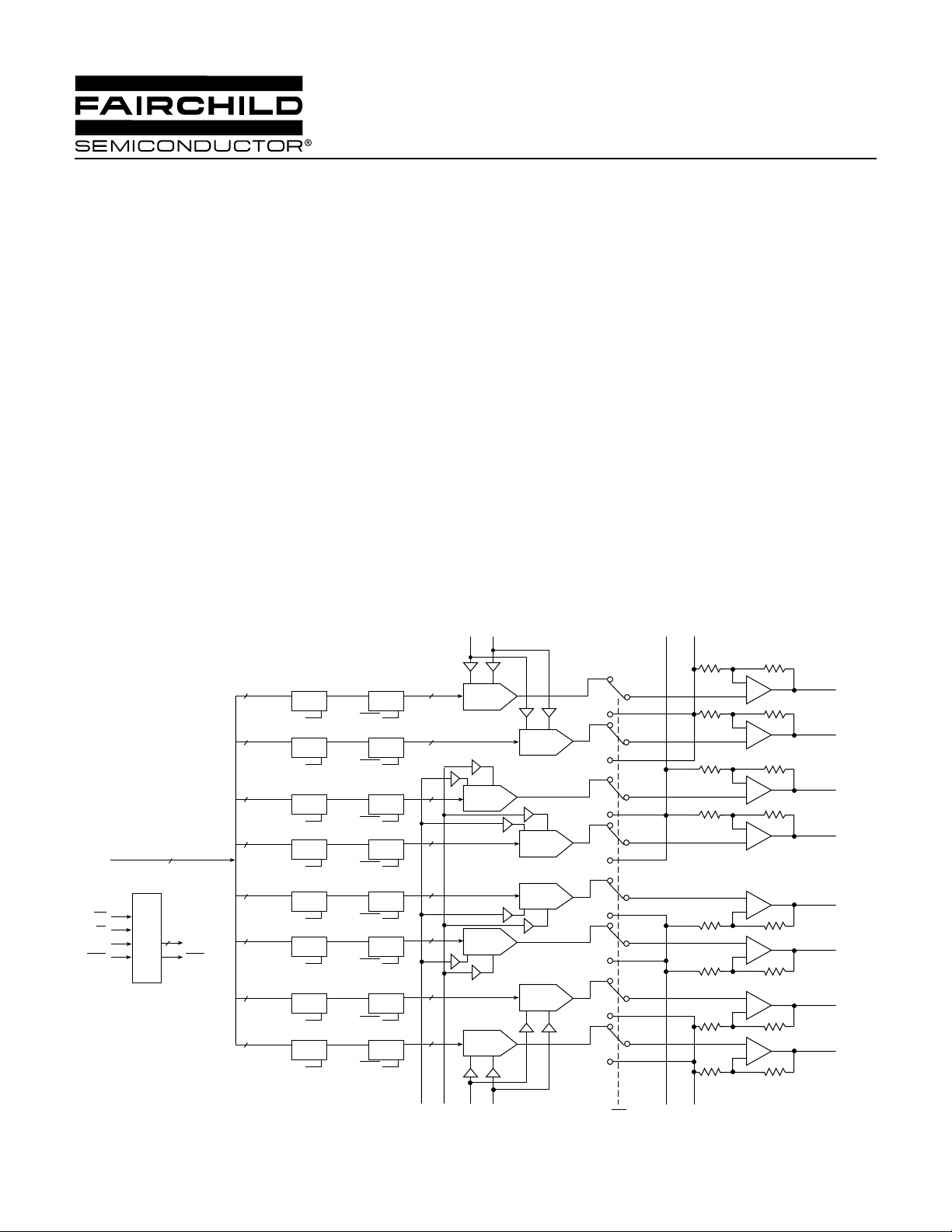
BLOCK DIAGRAM
D0D12
A0A2
LDAC
WR
13 13
13 13
13 13
13
CS
Control
8
Logic
LEA0LEA7
LDAC
13
13
13
DQ
0A 0B
LE
LEA0
DQ
1A 1B
LE
LEA1
DQ
2A 2B
LE
LEA2
DQ
3A 3B
LE
LEA3
DQ
4A 4B
LE
LEA4
Q
D
5A 5B
LE
LEA5
DQ
LDAC
DQ
LDAC
DQ
LDAC
DQ
LDAC
DQ
LDAC
D
LDAC
LE
LE
LE
13
LE
13
LE
13
Q
LE
APPLICATIONS
• Automatic test equipment
• Instrumentation
• Process control
DAC’s full-scale output voltage and output voltage offset
are adjustable with analog inputs (RGND, V
The SPT5420 operates over an industrial temperature
range of –40 °C to +85 °C and is availab le in a 10 x 10 mm,
44-lead metric quad flat pack (MQFP) plastic package.
V
REFT01VREFB01
DAC0
DAC2
DAC5
DAC1
DAC3
DAC4
RGND
RGND
01
23
REFB
-
+
-
+
-
+
-
+
+
-
+
-
, V
REFT
VOUT0
VOUT1
VOUT2
VOUT3
VOUT4
VOUT5
).
LE
LE
V
REFT2345
13
13
V
REFB2345VREFT67
DAC7
V
REFB67
DAC6
CLR
RGND
+
-
+
-
RGND
67
45
VOUT6
VOUT7
13
13
DQ
6A 6B
LE
LEA6
DQ
7A 7B
LE
LEA7
DQ
LDAC
DQ
LDAC

ABSOLUTE MAXIMUM RATINGS (Beyond which damage may occur)1 25 °C
Supply Voltages
VCC........................................................................+6 V
VDD......................................................................+15 V
Temperature
Operating Temperature .......................... –40 to +85 °C
Storage ................................................ –65 to +150 °C
VSS...................................................................... –15 V
Input Voltages
V
.................................... VSS –0.3 V to VDD +0.3 V
REFT
V
................................... VDD +0.3 V to VSS –0.3 V
REFB
Note: 1. Operation at any Absolute Maximum Rating is not implied. See
Electrical Specifications for proper nominal applied conditions
in typical applications.
Digital inputs....................................–0.3 V to VCC +0.3 V
ELECTRICAL SPECIFICATIONS
TA = T
PARAMETERS CONDITIONS LEVEL MIN TYP MAX UNITS
Accuracy
Reference Inputs
RGND Inputs
to T
MIN
, VCC = +5.0 V, VDD = +11.5 V, VSS = –8.0 V, V
MAX
REFT
=3.5 V , V
= –1.5 V, RL = +10 kΩ, CL = 50 pF, unless otherwise specified.
REFB
TEST TEST SPT5420
Resolution VI 13 Bits
Integral Linearity Error (ILE) VI –2.0 ±0.5 +2.0 LSB
Differential Linearity Error (DLE) VI –1.0 ±0.3 +1.0 LSB
Zero-Scale Error VI –25 +25 mV
Full Scale Error VI –25 +25 mV
Gain Error VI –25 +25 mV
Input Current IV ±100 nA
V
V
REFT
REFB
1
2
VI 0 +3.5 +5.0 V
VI –5.0 –1.5 0 V
DC Input Impedance V 60 kΩ
Input Range IV –2.0 2.0 V
Output Characteristics
Output Swing
3,4
VI +7/–3 V
Short Circuit Current IV 1 5 mA
Resistive Load VI 5 kΩ
DC Output Impedance IV 1.0 Ω
Digital Inputs
Logic 1 Voltage VI 2. 4 V
Logic 0 Voltage VI 0.8 V
Maximum Input Current VI –10 10 µA/pin
Input Capacitance V 10 pF
Notes:
1. V
< 8 V + (VSS x 0.5); e.g., if VSS = –8 V, then V
REFT
2. V
> (VDD x 0.5) – 9.5 V; e.g., if VDD = 11 V, then V
REFB
3. VSS + 2.5 V ≤ V
VSS + 2.5 V ≤ V
4. V
= 2 X (V
OUT
≤ VSS + 16.0 V for 18.5 V ≤ VDD – VSS ≤ 20.0 V
OUT
≤ VDD – 2.5 V f or VDD – VSS ≤ 18.5 V
OUT
REFB
+[V
REFT
– V
REFB
INPUT CODE
] X
8192
REFT
REFB
) – V
< 4 V
> –4 V
RGND
SPT5420
2 6/26/01
ELECTRICAL SPECIFICATIONS
TA = T
MIN
to T
, VCC = +5.0 V, VDD = +11.5 V, VSS = –8.0 V , V
MAX
REFT
=3.5 V, V
=–1.5 V, RL = +10 kΩ, CL = 50 pF, unless otherwise specified.
REFB
TEST TEST SPT5420
PARAMETERS CONDITIONS LEVEL MIN TYP MAX UNITS
Power Requirements
V
Supply Voltage (Digital) IV 4.75 5 5.25 V
CC
Supply Voltage (Analog)
V
DD
Supply Voltage (Analog)
V
SS
I
Supply Current VI 0.5 mA
CC
Supply Current Outputs Unloaded VI 5 10 mA
I
DD
Supply Current Outputs Unloaded VI 5 10 mA
I
SS
Power Supply Rejection Ratio ∆V
1,2
1,2
VI 5 11.5 12.5 V
VI –12.5 –8 –5V
/ ∆Full Scale IV 80 dB
DD
/ ∆Full Scale IV 80 dB
∆V
SS
Dynamic Performance
Output Settling Time
3
(Full Scale Change to ±0.5 LSB) CL ≤ 220 pF IV 15 µs
Slew Rate V 2.0 V/µs
Glitch Impulse V 35 nV-s
Channel to Channel Isolation V 100 dB
DAC to DAC Crosstalk V 40 nV-s
Digital Crosstalk V 1 nV-s
Digital Feedthrough V 1 nV-s
Timing Characteristics
(See page 4) IV
1. Supplies should provide 2.5 V headroom above and below max output s wing.
2. VDD – VSS ≤ 20 V
3. Output can drive 10,000 pF without oscillation, but with settling time degradation.
DEFINITION OF SELECTED TERMINOLOGY
Channel-to-Channel Isolation
Channel-to-Channel isolation refers to the proportion of input signal from one DAC’s reference input that appears at the output of
the other DAC. It is expressed in dBs.
DAC-to-DAC Crosstalk
DAC-to-DAC crosstalk is defined as the glitch impulse that appears at one DAC’s output due to both the digital change and subsequent analog output change at any other DAC. It is specified in nV-s.
Digital Crosstalk
The glitch impulse transferred to one DAC’s output due to a change in digital input code of any other DAC. It is specified in nV-s.
Digital Feedthrough
Digital feedthrough is the noise at a DAC’s output caused by changes to D0–D12 while WR is high.
TEST LEVEL CODES
All electrical characteristics are subject to the
following conditions:
All parameters having min/max specifications
are guaranteed. The Test Level column indicates the specific device testing actually performed during production and Quality Assurance inspection. Any blank section in the data
column indicates that the specification is not
tested at the specified condition.
LEVEL TEST PROCEDURE
I 100% production tested at the specified temperature.
II 100% production tested at T
specified temperatures.
III QA sample tested only at the specified temperatures.
IV Parameter is guaranteed (but not tested) by design and characteri-
zation data.
V Parameter is a typical value for infor mation purposes only.
VI 100% production tested at TA = +25 °C. Parameter is guaranteed
over specified temperature range.
= +25 °C, and sample tested at the
A
SPT5420
3 6/26/01
 Loading...