

Fairchild Semiconductor SI6943DQ Datasheet
Sept 2001
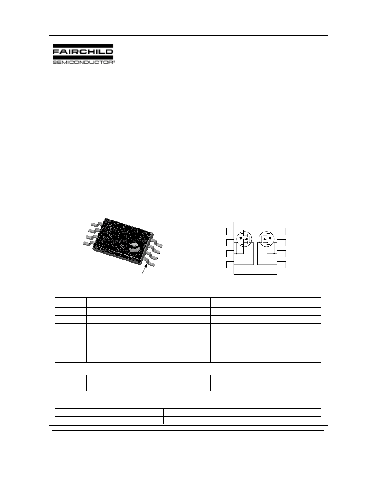
Si6943DQ
Dual P-Channel 2.5V Specified PowerTrench
MOSFET
Si6943DQ
General Description
This P-Channel –2.5V specif ied MOSFET is a rugged
gate version of Fairchild's Semiconductor’s advanced
PowerTrench process. It has been opt imized for power
management applications with a wide range of gate
drive voltage (–2.5V to –8V).
Applications
• Load switch
• Motor drive
• DC/DC conversion
• Power management
G
2
S
2
S
2
D
2
G
1
S
1
S
1
D
1
TSSOP-8
Pin 1
Features
• –2.5 A, –12 V, R
R
• Extended V
• Low gate charge (4.6nC typical)
• High performance trench te chnology for extremely
low R
DS(ON)
• Low profile TSSOP-8 package
range (±8V) for battery applications
GSS
1
2
3
4
= 110 mΩ @ VGS = –4.5 V.
DS(ON)
= 180 mΩ @ VGS = –2.5V.
DS(ON)
8
7
6
5
Absolute Maximum Ratings T
o
=25
C unless otherwise noted
A
Symbol Parameter Ratings Units
V
Drain-Source Voltage –12 V
DSS
V
Gate-Source Voltage
GSS
ID Drain Current – Continuous (Note 1) –2.5 A
– Pulsed –20
PD Power Dissipation for Single Operation (Note 1a) 1.0 W
TJ, T
STG
(Note 1b)
Operating and Storage Junction Temperature Range –55 to +150
±8
0.6
V
°C
Thermal Characteristics
R
θJA
Thermal Resistance, Junction-to-Ambient
(Note 1b)
(Note 1a) 100
125
°C/W
Package Marking and Ordering Information
Device Marking Device Reel Size Tape width Quantity
6943 Si6943DQ 13’’ 12mm 2500 units
2001 Fairchild Semiconductor Corporation
Si6943DQ Rev. B ( W)
Si6943DQ
Electrical Characteristics T
= 25°C unless otherwise noted
A
Symbol Parameter Test Conditions Min Typ Max Units
Off Characteristics
BV
Drain–Source Breakdown Voltage
DSS
∆BVDSS
∆T
I
Zero Gate Voltage Drain Current VDS = –12 V, VGS = 0 V –1
DSS
I
GSSF
I
GSSR
Breakdown Voltage Temperature
Coefficient
J
Gate–Body Leakage, Forward VGS = –8 V, VDS = 0 V –100 nA
Gate–Body Leakage, Reverse VGS = 8 V, VDS = 0 V 100 nA
V
= 0 V, ID = –250 µA
GS
I
= –250 µA, Referenced to 25°C
D
–12 V
–13
mV/°C
µA
On Characteristics (Note 2)
V
Gate Threshold Voltage
GS(th)
∆VGS(th)
∆TJ
R
DS(on)
Gate Threshold Voltage
Temperature Coefficient
Static Drain–Source
On–Resistance
I
On–State Drain Current VGS = –4.5 V, VDS = –5 V –10 A
D(on)
V
= VGS, ID = –250 µA
DS
I
= –250 µA, Referenced to 25°C
D
VGS = –4.5 V, ID = –2.5 A
V
= –2.5 V, ID = –1.9 A
GS
= –4.5 V, ID = –2.5 A, TJ=125°C
V
GS
–0.6 –0.9 –1.5 V
3
89
125
116
110
180
154
mV/°C
mΩ
gFS Forward Transconductance VDS = –9 V, ID = –2.5 A 7 S
Dynamic Characteristics
C
Input Capacitance 509 pF
iss
C
Output Capacitance 97 pF
oss
C
Reverse Transfer Capacitance
rss
V
= –6 V, V
DS
f = 1.0 MHz
GS
= 0 V,
43 pF
Switching Characteristics (Note 2)
V
= –6 V, ID = –1 A,
t
Turn–On Delay Time 9 18 ns
d(on)
tr Turn–On Rise Time 12 22 ns
t
Turn–Off Delay Time 17 31 ns
d(off)
tf Turn–Off Fall Time
Qg Total Gate Charge 4.6 6.4 nC
Qgs Gate–Source Charge 1.1 nC
Qgd Gate–Drain Charge
DD
= –4.5 V, R
V
GS
V
= –6V, ID = –2.5 A,
DS
= –4.5 V
V
GS
GEN
= 6 Ω
8 16 ns
0.7 nC
Drain–Source Diode Characteristics and Maximum Ratings
IS Maximum Continuous Drain–Source Diode Forward Current –1 A
VSD Drain–Source Diode Forward
Voltage
Notes:
1. R
is the sum of the junction-to-case and case-to-ambient thermal resistance where the case thermal reference is defined as the solder mounting surface of
θJA
the drain pins. R
a) R
is 100°C/W (steady state) when mounted on a 1 inch² copper pad on FR-4.
θJA
is 125°C/W (steady state) when mounted on a minimum copper pad on FR-4.
b) R
θJA
2. Pulse Test: Pulse Width < 300µs, Duty Cycle < 2.0%
is guaranteed by design while R
θJC
θCA
VGS = 0 V, IS = –1 A (Note 2) 0.8 –1.2 V
is determined by the user's board design.
Si6943DQ Rev. B ( W)
 Loading...